 | ÐлекÑÑоннÑй компоненÑ: LTC2444 | СкаÑаÑÑ:  PDF PDF  ZIP ZIP |
Äîêóìåíòàöèÿ è îïèñàíèÿ www.docs.chipfind.ru
LTC2444/LTC2445/
LTC2448/LTC2449
1
sn2444589 2444589fs
FEATURES
DESCRIPTIO
U
APPLICATIO S
U
TYPICAL APPLICATIO
U
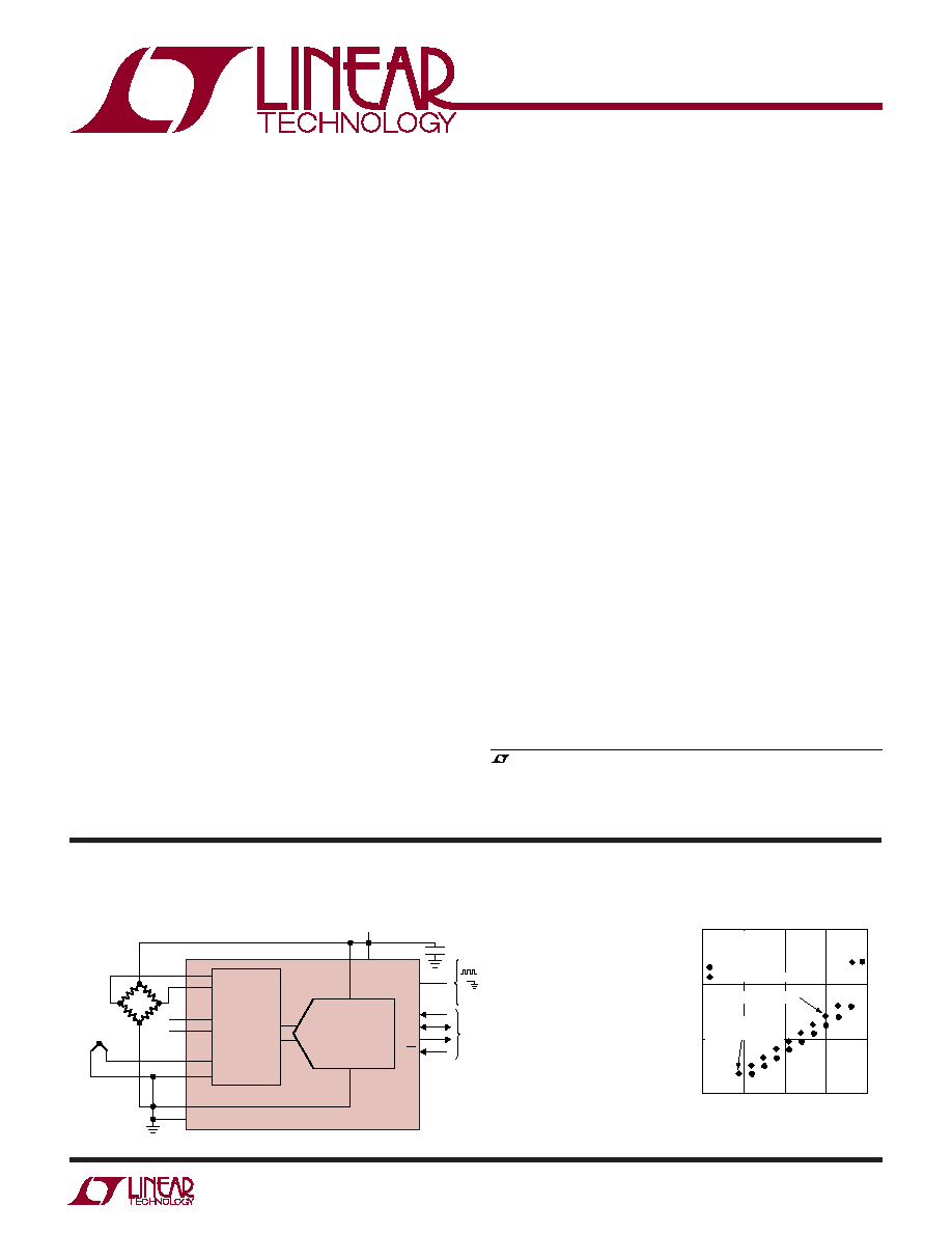
High Speed Multiplexing
Weight Scales
Auto Ranging 6-Digit DVMs
Direct Temperature Measurement
High Speed Data Acquisition
Up to 8 Differential or 16 Single-Ended Input
Channels
Up to 8kHz Output Rate
Up to 4kHz Multiplexing Rate
Selectable Speed/Resolution
2µV
RMS
Noise at 1.76kHz Output Rate
200nV
RMS
Noise at 13.8Hz Output Rate with
Simultaneous 50/60Hz Rejection
Guaranteed Modulator Stability and Lock-Up
Immunity for any Input and Reference Conditions
0.0005% INL, No Missing Codes
Autosleep Enables 20µA Operation at 6.9Hz
< 5µV Offset (4.5V < V
CC
< 5.5V, 40°C to 85°C)
Differential Input and Differential Reference with
GND to V
CC
Common Mode Range
No Latency Mode, Each Conversion is Accurate Even
After a New Channel is Selected
Internal Oscillator--No External Components
LTC2445/LTC2449 Include MUXOUT/ADCIN for
External Buffering or Gain
Tiny QFN 5mm x 7mm Package
24-Bit High Speed
8-/16-Channel ADCs with
Selectable Speed/Resolution
The LTC
®
2444/LTC2445/LTC2448/LTC2449 are 8-/16-
channel (4-/8-differential) high speed 24-bit No Latency
TM
ADCs. They use a proprietary delta-sigma architec-
ture enabling variable speed/resolution. Through a simple
4-wire serial interface, ten speed/resolution combinations
6.9Hz/280nV
RMS
to 3.5kHz/25µV
RMS
(4kHz with external
oscillator) can be selected with no latency between con-
version results or shift in DC accuracy (offset, full-scale,
linearity, drift). Additionally, a 2X speed mode can be
selected enabling output rates up to 7kHz (8kHz if an
external oscillator is used) with one cycle latency.
Any combination of single-ended or differential inputs can
be selected with a common mode input range from ground
to V
CC
, independent of V
REF
. While operating in the 1X
speed mode the first conversion following a new speed,
resolution, or channel selection is valid. Since there is no
settling time between conversions, all 8 differential chan-
nels can be scanned at a rate of 500Hz. At the conclusion
of each conversion, the converter is internally reset elimi-
nating any memory effects between successive conver-
sions and assuring stability of the high order delta-sigma
modulator.
, LTC and LT are registered trademarks of Linear Technology Corporation.
LTC2444/LTC2448
Speed vs RMS Noise
Simple 24-Bit Variable Speed Data Acquisition System
SDI
SCK
SDO
CS
F
O
REF
+
V
CC
4.5V TO 5.5V
1µF
COM
REF
GND
THERMOCOUPLE
VARIABLE SPEED/
RESOLUTION
DIFFERENTIAL
24-BIT ADC
16-CHANNEL
MUX
+
2444 TA01
4-WIRE
SPI INTERFACE
LTC2448
= EXTERNAL OSCILLATOR
= INTERNAL OSCILLATOR
(SIMULTANEOUS 50Hz/60Hz
REJECTION AT 6.9Hz OUTPUT RATE)
CH0
CH1
·
·
·
·
·
·
CH7
CH8
CH15
CONVERSION RATE (Hz)
1
0.1
RMS NOISE (
µ
V)
1
10
100
10
100
2440 TA02
1000
10000
2.8µV AT 880Hz
280nV AT 6.9Hz
(50/60Hz REJECTION)
V
CC
= 5V
V
REF
= 5V
V
IN
+
= V
IN
= 0V
2X SPEED MODE
NO LATENCY MODE
No Latency is a trademark of Linear Technology Corporation.
LTC2444/LTC2445/
LTC2448/LTC2449
2
sn2444589 2444589fs
ORDER PART
NUMBER
ORDER PART
NUMBER
ABSOLUTE AXI U
RATI GS
W
W
W
U
PACKAGE/ORDER I FOR ATIO
U
U
W
(Notes 1, 2)
Supply Voltage (V
CC
) to GND ....................... 0.3V to 6V
Analog Input Pins Voltage
to GND .................................... 0.3V to (V
CC
+ 0.3V)
Reference Input Pins Voltage
to GND .................................... 0.3V to (V
CC
+ 0.3V)
Digital Input Voltage to GND ........ 0.3V to (V
CC
+ 0.3V)
Digital Output Voltage to GND ..... 0.3V to (V
CC
+ 0.3V)
T
JMAX
= 125°C,
JA
= 34°C/W
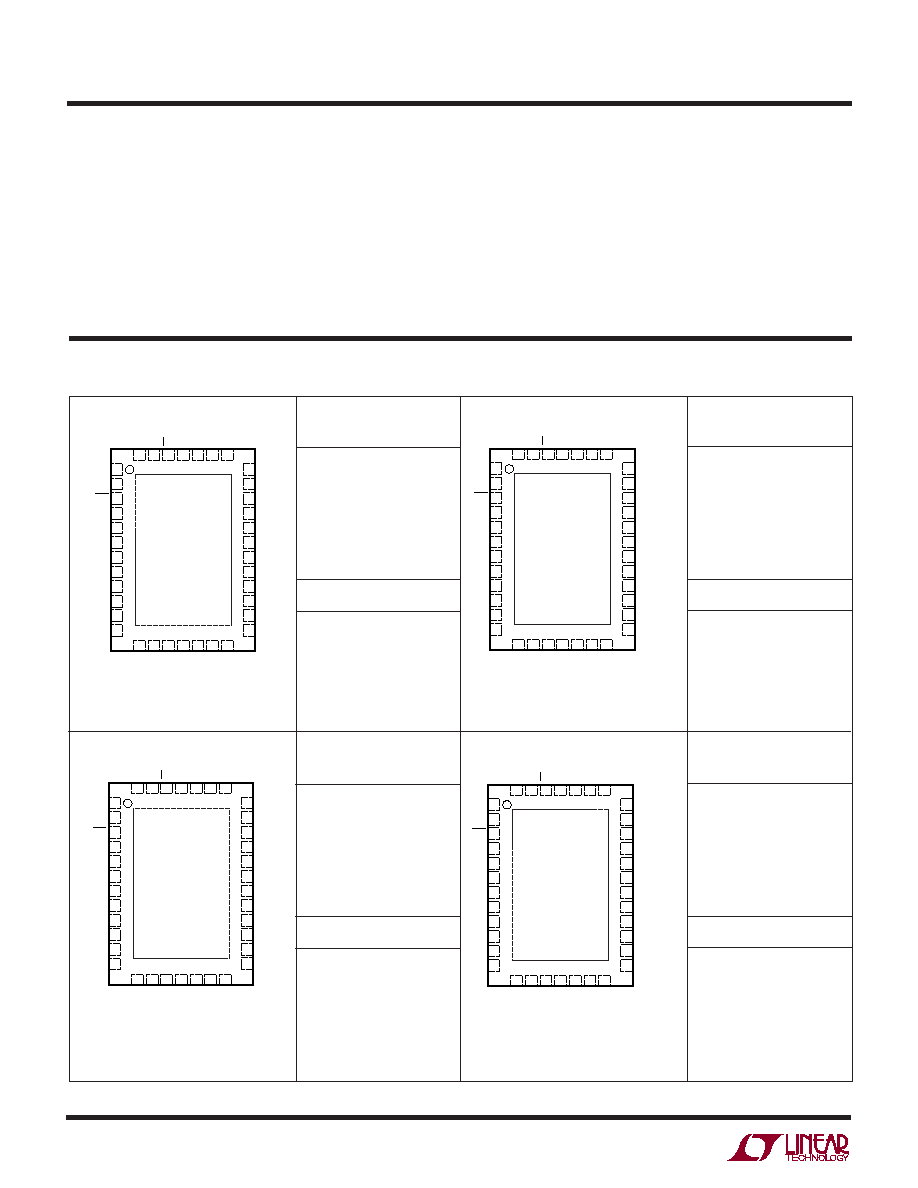
LTC2444CUHF
LTC2444IUHF
QFN PART MARKING*
2444
Operating Temperature Range
LTC2444C/LTC2445C/
LTC2448C/LTC2449C .............................. 0°C to 70°C
LTC2444I/LTC2445I/
LTC2448I/LTC2449I ........................... 40°C to 85°C
Storage Temperature Range ................. 65°C to 125°C
LTC2448CUHF
LTC2448IUHF
QFN PART MARKING*
2448
13 14 15 16
TOP VIEW
UHF PACKAGE
38-LEAD (5mm × 7mm) PLASTIC QFN
17 18 19
38 37 36 35 34 33 32
24
25
26
27
28
29
30
31
8
7
6
5
4
3
2
1
GND
BUSY
EXT
GND
GND
GND
COM
NC
CH0
CH1
NC
NC
GND
REF
REF
+
V
CC
NC
NC
NC
NC
NC
CH7
CH6
NC
SCK
SDO
CS
F
O
SDI
GND
GND
CH2
CH3
NC
NC
CH4
CH5
NC
23
22
21
20
9
10
11
12
13 14 15 16
TOP VIEW
UHF PACKAGE
38-LEAD (5mm × 7mm) PLASTIC QFN
17 18 19
38 37 36 35 34 33 32
24
25
26
27
28
29
30
31
8
7
6
5
4
3
2
1
GND
BUSY
EXT
GND
GND
GND
COM
CH0
CH1
CH2
CH3
CH4
GND
REF
REF
+
V
CC
NC
NC
NC
NC
CH15
CH14
CH13
CH12
SCK
SDO
CS
F
O
SDI
GND
GND
CH5
CH6
CH7
CH8
CH9
CH10
CH11
23
22
21
20
9
10
11
12
T
JMAX
= 125°C,
JA
= 34°C/W
ORDER PART
NUMBER
ORDER PART
NUMBER
T
JMAX
= 125°C,
JA
= 34°C/W
LTC2445CUHF
LTC2445IUHF
QFN PART MARKING*
2445
*The temperature grade is identified by a label on the shipping container. Consult LTC Marketing for parts specified with wider operating temperature ranges.
LTC2449CUHF
LTC2449IUHF
QFN PART MARKING*
2449
T
JMAX
= 125°C,
JA
= 34°C/W
13 14 15 16
TOP VIEW
UHF PACKAGE
38-LEAD (5mm × 7mm) PLASTIC QFN
17 18 19
38 37 36 35 34 33 32
24
25
26
27
28
29
30
31
8
7
6
5
4
3
2
1
GND
BUSY
EXT
GND
GND
GND
COM
NC
CH0
CH1
NC
NC
GND
REF
REF
+
V
CC
MUXOUTN
ADCINN
ADCINP
MUXOUTP
NC
CH7
CH6
NC
SCK
SDO
CS
F
O
SDI
GND
GND
CH2
CH3
NC
NC
CH4
CH5
NC
23
22
21
20
9
10
11
12
13 14 15 16
TOP VIEW
UHF PACKAGE
38-LEAD (5mm × 7mm) PLASTIC QFN
17 18 19
38 37 36 35 34 33 32
24
25
26
27
28
29
30
31
8
7
6
5
4
3
2
1
GND
BUSY
EXT
GND
GND
GND
COM
CH0
CH1
CH2
CH3
CH4
GND
REF
REF
+
V
CC
MUXOUTN
ADCINN
ADCINP
MUXOUTP
CH15
CH14
CH13
CH12
SCK
SDO
CS
F
O
SDI
GND
GND
CH5
CH6
CH7
CH8
CH9
CH10
CH11
23
22
21
20
9
10
11
12
LTC2444/LTC2445/
LTC2448/LTC2449
3
sn2444589 2444589fs
ELECTRICAL CHARACTERISTICS
PARAMETER
CONDITIONS
MIN
TYP
MAX
UNITS
Resolution (No Missing Codes)
0.1V V
REF
V
CC
, 0.5 · V
REF
V
IN
0.5 · V
REF
, (Note 5)
24
Bits
Integral Nonlinearity
V
CC
= 5V, REF
+
= 5V, REF
= GND, V
INCM
= 2.5V, (Note 6)
5
15
ppm of V
REF
REF
+
= 2.5V, REF
= GND, V
INCM
= 1.25V, (Note 6)
3
ppm of V
REF
Offset Error
2.5V REF
+
V
CC
, REF
= GND,
2.5
5
µV
GND IN
+
= IN
V
CC
(Note 12)
Offset Error Drift
2.5V REF
+
V
CC
, REF
= GND,
20
nV/°C
GND IN
+
= IN
V
CC
Positive Full-Scale Error
REF
+
= 5V, REF
= GND, IN
+
= 3.75V, IN
= 1.25V
10
50
ppm of V
REF
REF
+
= 2.5V, REF
= GND, IN
+
= 1.875V, IN
= 0.625V
10
50
ppm of V
REF
Positive Full-Scale Error Drift
2.5V REF
+
V
CC
, REF
= GND,
0.2
ppm of V
REF
/°C
IN
+
= 0.75REF
+
, IN
= 0.25 · REF
+
Negative Full-Scale Error
REF
+
= 5V, REF
= GND, IN
+
= 1.25V, IN
= 3.75V
10
50
ppm of V
REF
REF
+
= 2.5V, REF
= GND, IN
+
= 0.625V, IN
= 1.875V
10
50
ppm of V
REF
Negative Full-Scale Error Drift
2.5V REF
+
V
CC
, REF
= GND,
0.2
ppm of V
REF
/°C
IN
+
= 0.25 · REF
+
, IN
= 0.75 · REF
+
Total Unadjusted Error
5V V
CC
5.5V, REF
+
= 2.5V, REF
= GND, V
INCM
= 1.25V
15
ppm of V
REF
5V V
CC
5.5V, REF
+
= 5V, REF
= GND, V
INCM
= 2.5V
15
ppm of V
REF
REF
+
= 2.5V, REF
= GND, V
INCM
= 1.25V, (Note 6)
15
ppm of V
REF
Input Common Mode Rejection DC
2.5V REF
+
V
CC
, REF
= GND,
120
dB
GND IN
= IN
+
V
CC
The
denotes specifications which apply over the full operating
temperature range, otherwise specifications are at T
A
= 25°C. (Notes 3, 4)
SYMBOL
PARAMETER
CONDITIONS
MIN
TYP
MAX
UNITS
IN
+
Absolute/Common Mode IN
+
Voltage
GND 0.3V
V
CC
+ 0.3V
V
IN
Absolute/Common Mode IN
Voltage
GND 0.3V
V
CC
+ 0.3V
V
V
IN
Input Differential Voltage Range
V
REF
/2
V
REF
/2
V
(IN
+
IN
)
REF
+
Absolute/Common Mode REF
+
Voltage
0.1
V
CC
V
REF
Absolute/Common Mode REF
Voltage
GND
V
CC
0.1V
V
V
REF
Reference Differential Voltage Range
0.1
V
CC
V
(REF
+
REF
)
C
S(IN+)
IN
+
Sampling Capacitance
2
pF
C
S(IN)
IN
Sampling Capacitance
2
pF
C
S(REF+)
REF
+
Sampling Capacitance
2
pF
C
S(REF)
REF
Sampling Capacitance
2
pF
I
DC_LEAK(IN+, IN,
Leakage Current, Inputs and Reference
CS = V
CC
, IN
+
= GND, IN
= GND,
15
1
15
nA
REF+, REF)
REF
+
= 5V, REF
= GND
I
SAMPLE(IN+, IN,
Average Input/Reference Current
Varies, See Applications Section
nA
REF+, REF)
During Sampling
t
OPEN
MUX Break-Before-Make
50
ns
QIRR
MUX Off Isolation
V
IN
= 2V
P-P
DC to 1.8MHz
120
dB
The
denotes specifications which apply over the full operating
temperature range, otherwise specifications are at T
A
= 25°C. (Note 3)
A ALOG I PUT A
U
D REFERE CE
U
U
U
LTC2444/LTC2445/
LTC2448/LTC2449
4
sn2444589 2444589fs
TI I G CHARACTERISTICS
U
W
SYMBOL
PARAMETER
CONDITIONS
MIN
TYP
MAX
UNITS
V
CC
Supply Voltage
4.5
5.5
V
I
CC
Supply Current
Conversion Mode
CS = 0V (Note 7)
8
11
mA
Sleep Mode
CS = V
CC
(Note 7)
8
30
µA
The
denotes specifications which apply over the full operating temperature range,
otherwise specifications are at T
A
= 25°C. (Note 3)
POWER REQUIRE E TS
W
U
The
denotes specifications which apply over the full
operating temperature range, otherwise specifications are at T
A
= 25°C. (Note 3)
SYMBOL
PARAMETER
CONDITIONS
MIN
TYP
MAX
UNITS
V
IH
High Level Input Voltage
4.5V V
CC
5.5V
2.5
V
CS, F
O
V
IL
Low Level Input Voltage
4.5V V
CC
5.5V
0.8
V
CS, F
O
V
IH
High Level Input Voltage
4.5V V
CC
5.5V (Note 8)
2.5
V
SCK
V
IL
Low Level Input Voltage
4.5V V
CC
5.5V (Note 8)
0.8
V
SCK
I
IN
Digital Input Current
0V V
IN
V
CC
10
10
µA
CS, F
O
, EXT, SOI
I
IN
Digital Input Current
0V V
IN
V
CC
(Note 8)
10
10
µA
SCK
C
IN
Digital Input Capacitance
10
pF
CS, F
O
C
IN
Digital Input Capacitance
(Note 8)
10
pF
SCK
V
OH
High Level Output Voltage
I
O
= 800µA
V
CC
0.5V
V
SDO, BUSY
V
OL
Low Level Output Voltage
I
O
= 1.6mA
0.4V
V
SDO, BUSY
V
OH
High Level Output Voltage
I
O
= 800µA (Note 9)
V
CC
0.5V
V
SCK
V
OL
Low Level Output Voltage
I
O
= 1.6mA (Note 9)
0.4V
V
SCK
I
OZ
Hi-Z Output Leakage
10
10
µA
SDO
DIGITAL I PUTS A D DIGITAL OUTPUTS
U
U
The
denotes specifications which apply over the full operating temperature
range, otherwise specifications are at T
A
= 25°C. (Note 3)
SYMBOL
PARAMETER
CONDITIONS
MIN
TYP
MAX
UNITS
f
EOSC
External Oscillator Frequency Range
0.1
20
MHz
t
HEO
External Oscillator High Period
25
10000
ns
t
LEO
External Oscillator Low Period
25
10000
ns
t
CONV
Conversion Time
OSR = 256 (SDI = 0)
0.99
1.13
1.33
ms
OSR = 32768 (SDI = 1)
126
145
170
ms
External Oscillator (Notes 10, 13)
40 · OSR +170
f
EOSC
(kHz)
ms
f
ISCK
Internal SCK Frequency
Internal Oscillator (Note 9)
0.8
0.9
1
MHz
External Oscillator (Notes 9, 10)
f
EOSC
/10
Hz
LTC2444/LTC2445/
LTC2448/LTC2449
5
sn2444589 2444589fs
SYMBOL
PARAMETER
CONDITIONS
MIN
TYP
MAX
UNITS
D
ISCK
Internal SCK Duty Cycle
(Note 9)
45
55
%
f
ESCK
External SCK Frequency Range
(Note 8)
20
MHz
t
LESCK
External SCK Low Period
(Note 8)
25
ns
t
HESCK
External SCK High Period
(Note 8)
25
ns
t
DOUT_ISCK
Internal SCK 32-Bit Data Output Time
Internal Oscillator (Notes 9, 11)
41.6
35.3
30.9
µs
External Oscillator (Notes 9, 10)
320/f
EOSC
s
t
DOUT_ESCK
External SCK 32-Bit Data Output Time
(Note 8)
32/f
ESCK
s
t
1
CS to SDO Low Z
(Note 12)
0
25
ns
t
2
CS to SDO High Z
(Note 12)
0
25
ns
t
3
CS to SCK
(Note 9)
5
µs
t
4
CS to SCK
(Notes 8, 12)
25
ns
t
KQMAX
SCK to SDO Valid
25
ns
t
KQMIN
SDO Hold After SCK
(Note 5)
15
ns
t
5
SCK Set-Up Before CS
50
ns
t
6
SCK Hold After CS
50
ns
t
7
SDI Setup Before SCK
(Note 5)
10
ns
t
8
SDI Hold After SCK
(Note 5)
10
ns
The
denotes specifications which apply over the full operating temperature
range, otherwise specifications are at T
A
= 25°C. (Note 3)
TI I G CHARACTERISTICS
W
U
GND (Pins 1, 4, 5, 6, 31, 32, 33): Ground. Multiple
ground pins internally connected for optimum ground
current flow and V
CC
decoupling. Connect each one of
these pins to a common ground plane through a low
impedance connection. All 7 pins must be connected to
ground for proper operation.
BUSY (Pin 2): Conversion in Progress Indicator. This pin
is HIGH while the conversion is in progress and goes LOW
indicating the conversion is complete and data is ready. It
remains LOW during the sleep and data output states. At
the conclusion of the data output state, it goes HIGH
indicating a new conversion has begun.
EXT (Pin 3): Internal/External SCK Selection Pin. This pin
is used to select internal or external SCK for outputting/
inputting data. If EXT is tied low, the device is in the
external SCK mode and data is shifted out of the device
under the control of a user applied serial clock. If EXT is
tied high, the internal serial clock mode is selected. The
device generates its own SCK signal and outputs this on
the SCK pin. A framing signal BUSY (Pin 2) goes low
indicating data is being output.
COM (Pin 7): The common negative input (IN
) for all
single ended multiplexer configurations. The voltage on
CH0-CH15 and COM pins can have any value between
U
U
U
PI FU CTIO S
Note 1: Absolute Maximum Ratings are those values beyond which the life
of the device may be impaired.
Note 2: All voltage values are with respect to GND.
Note 3: V
CC
= 4.5V to 5.5V unless otherwise specified.
V
REF
= REF
+
REF
, V
REFCM
= (REF
+
+ REF
)/2;
V
IN
= IN
+
IN
, V
INCM
= (IN
+
+ IN
)/2.
Note 4: F
O
pin tied to GND or to external conversion clock source with
f
EOSC
= 10MHz unless otherwise specified.
Note 5: Guaranteed by design, not subject to test.
Note 6: Integral nonlinearity is defined as the deviation of a code from a
straight line passing through the actual endpoints of the transfer curve.
The deviation is measured from the center of the quantization band.
Note 7: The converter uses the internal oscillator.
Note 8: The converter is in external SCK mode of operation such that the
SCK pin is used as a digital input. The frequency of the clock signal driving
SCK during the data output is f
ESCK
and is expressed in Hz.
Note 9: The converter is in internal SCK mode of operation such that the
SCK pin is used as a digital output. In this mode of operation, the SCK pin
has a total equivalent load capacitance of C
LOAD
= 20pF.
Note 10: The external oscillator is connected to the F
O
pin. The external
oscillator frequency, f
EOSC
, is expressed in Hz.
Note 11: The converter uses the internal oscillator. F
O
= 0V.
Note 12: Guaranteed by design and test correlation.
Note 13: There is an internal reset that adds an additional 1µs (typ) to the
conversion time.