 | ÐлекÑÑоннÑй компоненÑ: LTC4210 | СкаÑаÑÑ:  PDF PDF  ZIP ZIP |
421012i.pm6
1
LTC4210-1/LTC4210-2
421012f
APPLICATIO S
U
DESCRIPTIO
U
FEATURES
TYPICAL APPLICATIO
U
The LTC
®
4210 is a 6-pin SOT-23 Hot Swap
TM
controller
that allows a board to be safely inserted and removed from
a live backplane. An internal high side switch driver
controls the GATE of an external N-channel MOSFET for a
supply voltage ranging from 2.7V to 16.5V. The LTC4210
provides the initial timing cycle and allows the GATE to be
ramped up at an adjustable rate.
The LTC4210 features a fast current limit loop providing
active current limiting together with a circuit breaker
timer. The signal at the ON pin turns the part on and off and
is also used for the reset function.
This part is available in two options: the LTC4210-1 for
automatic retry on overcurrent fault and the LTC4210-2
for latch off on an overcurrent fault.
s
Allows Safe Board Insertion and Removal
from a Live Backplane
s
Adjustable Analog Current Limit
with Circuit Breaker
s
Fast Response Limits Peak Fault Current
s
Automatic Retry or Latch Off On Current Fault
s
Adjustable Supply Voltage Power-Up Rate
s
High Side Drive for External MOSFET Switch
s
Controls Supply Voltages from 2.7V to 16.5V
s
Undervoltage Lockout
s
Adjustable Overvoltage Protection
s
Low Profile (1mm) SOT-23 (ThinSOT
TM
) Package
s
Hot Board Insertion
s
Electronic Circuit Breaker
s
Industrial High Side Switch/Circuit Breaker
Hot Swap Controller in
6-Lead SOT-23 Package
, LTC and LT are registered trademarks of Linear Technology Corporation.
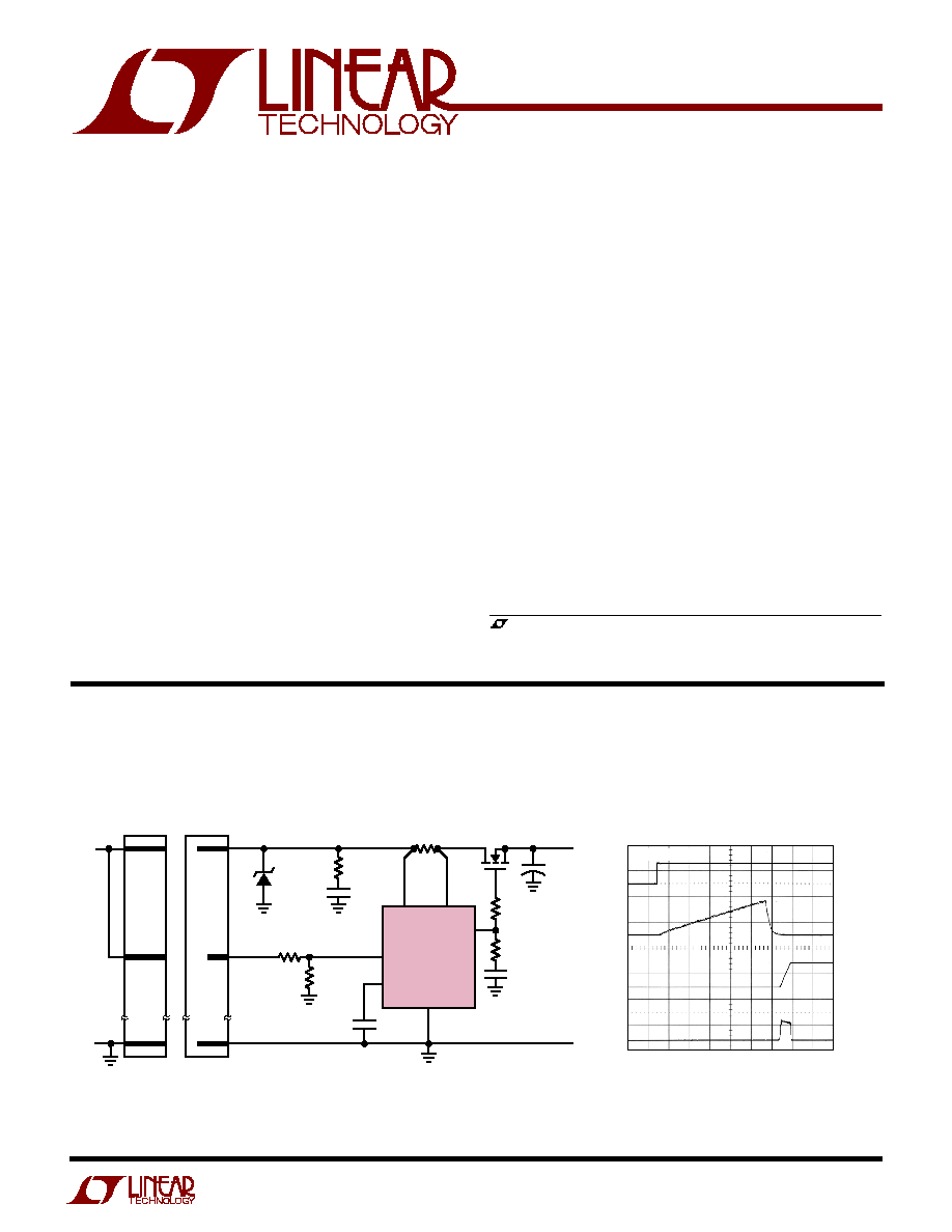
Single Channel 5V Hot Swap Controller
ThinSOT and Hot Swap are trademarks of Linear Technology Corporation.
Power-Up Sequence
+
V
CC
SENSE
LTC4210
470
µ
F
C
LOAD
V
OUT
5V
4A
GND
4210 TA01
R
C
100
GATE
GND
TIMER
ON
SHORT
LONG
V
IN
5V
GND
LONG
Z1: ISMA10A OR SMAJ10A
R
ON2
10k
R
ON1
20k
R
X
10
R
SENSE
0.01
PCB EDGE
CONNECTOR
(MALE)
Q1
Si4410DY
Z1
OPTIONAL
R
G
100
C
TIMER
0.22
µ
F
C
X
0.1
µ
F
C
C
0.01
µ
F
BACKPLANE
CONNECTOR
(FEMALE)
4210 TA02
10ms/DIV
I
OUT
(0.5A/DIV)
V
OUT
(5V/DIV)
V
ON
(2V/DIV)
V
TIMER
(1V/DIV)
C
LOAD
= 470
µ
F
2
LTC4210-1/LTC4210-2
421012f
(Note 1)
Supply Voltage (V
CC
) ............................................... 17V
Input Voltage (SENSE, TIMER) .. 0.3V to (V
CC
+ 0.3V)
Input Voltage (ON) ..................................... 0.3V to 17V
Output Voltage (GATE) ........ Internally Limited (Note 3)
Operating Temperature Range
LTC4210-1C/LTC4210-2C ....................... 0
°
C to 70
°
C
LTC4210-1I/LTC4210-2I .................... 40
°
C to 85
°
C
Storage Temperature Range ................. 65
°
C to 150
°
C
Lead Temperature (Soldering, 10 sec).................. 300
°
C
ABSOLUTE AXI U RATI GS
W
W
W
U
PACKAGE/ORDER I FOR ATIO
U
U
W
ORDER PART
NUMBER
LTC4210-1CS6
LTC4210-2CS6
LTC4210-1IS6
LTC4210-2IS6
T
JMAX
= 125
°
C,
JA
= 230
°
C/ W
TIMER 1
GND 2
ON 3
6 V
CC
5 SENSE
4 GATE
TOP VIEW
S6 PACKAGE
6-LEAD PLASTIC TSOT-23
S6 PART MARKING
LTYW
LTYX
LTF5
LTF6
Consult LTC Marketing for parts specified with wider operating temperature ranges.
SYMBOL
PARAMETER
CONDITIONS
MIN
TYP
MAX
UNITS
V
CC
Supply Voltage
q
2.7
16.5
V
I
CC
V
CC
Supply Current
q
0.65
3.5
mA
V
LKOR
V
CC
Undervoltage Lockout Release
V
CC
Rising
q
2.2
2.5
2.65
V
V
LKOHYST
V
CC
Undervoltage Lockout Hysteresis
100
mV
I
INON
ON Pin Input Current
q
10
0
10
µ
A
I
INSENSE
SENSE Pin Input Current
V
SENSE
= V
CC
q
10
5
10
µ
A
V
CB
Circuit Breaker Trip Voltage
V
CB
= (V
CC
V
SENSE
)
q
44
50
56
mV
I
GATEUP
GATE Pin Pull-Up Current
V
GATE
= 0V
q
5
10
15
µ
A
I
GATEDN
GATE Pin Pull-Down Current
V
TIMER
= 1.5V, V
GATE
= 3V or
25
mA
V
ON
= 0V, V
GATE
= 3V or
V
CC
V
SENSE
= 100mV, V
GATE
= 3V
V
GATE
External N-Channel Gate Drive
V
GATE
V
CC
, V
CC
= 2.7V
q
4.0
6.5
8
V
V
GATE
V
CC
, V
CC
= 3V
q
4.5
7.5
10
V
V
GATE
V
CC
, V
CC
= 3.3V
q
5.0
8.5
12
V
V
GATE
V
CC
, V
CC
= 5V
q
10
12
16
V
V
GATE
V
CC
, V
CC
= 12V
q
9.0
12
16
V
V
GATE
V
CC
, V
CC
= 15V
q
6.0
11
18
V
I
TIMERUP
TIMER Pin Pull-Up Current
Initial Cycle, V
TIMER
= 1V
q
2
5
8.5
µ
A
During Current Fault Condition, V
TIMER
= 1V
q
25
60
100
µ
A
I
TIMERDN
TIMER Pin Pull-Down Current
After Current Fault Disappears, V
TIMER
= 1V
q
2
3.5
µ
A
Under Normal Conditions, V
TIMER
= 1V
100
µ
A
V
TIMER
TIMER Pin Threshold
High Threshold, TIMER Rising
q
1.22
1.3
1.38
V
Low Threshold, TIMER Falling
q
0.15
0.2
0.25
V
V
TMRHYST
TIMER Low Threshold Hysteresis
100
mV
V
ON
ON Pin Threshold
ON Threshold, ON Rising
q
1.22
1.3
1.38
V
V
ONHYST
ON Pin Threshold Hysteresis
80
mV
The
q
denotes specifications which apply over the full operating
temperature range, otherwise specifications are T
A
= 25
°
C. V
CC
= 5V, unless otherwise noted. (Note 2)
ELECTRICAL CHARACTERISTICS
3
LTC4210-1/LTC4210-2
421012f
75
SUPPLY CURRENT (mA)
150
25
50
0
25
50
75 100 125
4.0
3.5
3.0
2.5
2.0
1.5
1.0
0.5
0
TEMPERATURE (
°
C)
75
UNDERVOLTAGE LOCKOUT THRESHOLD (V)
150
25
50
0
25
50
75 100 125
2.65
2.60
2.55
2.50
2.45
2.40
2.35
2.30
2.25
TEMPERATURE (
°
C)
75
V
GATE
(V)
150
25
50
0
25
50
75 100 125
40
35
30
25
20
15
10
5
0
TEMPERATURE (
°
C)
4210 G01
4210 G02
4210 G03
4210 G04
4210 G05
4210 G06
SUPPLY VOLTAGE (V)
0
SUPPLY CURRENT (mA)
4.0
3.5
3.0
2.5
2.0
1.5
1.0
0.5
0
16
4
2
6
10
14
18
8
12
20
T
A
= 25
°
C
SUPPLY VOLTAGE (V)
0
V
GATE
(V)
40
35
30
25
20
15
10
5
0
16
4
2
6
10
14
18
8
12
20
T
A
= 25
°
C
SUPPLY VOLTAGE (V)
0
I
GATEUP
(
µ
A)
8.0
8.5
9.0
9.5
10.0
10.5
11.0
11.5
12.0
16
4
2
6
10
14
18
8
12
20
T
A
= 25
°
C
V
CC
= 15V
V
CC
RISING
V
CC
FALLING
V
CC
= 12V
V
CC
= 5V
V
CC
= 3V
V
CC
= 15V
V
CC
= 12V
V
CC
= 5V
V
CC
= 3V
SYMBOL
PARAMETER
CONDITIONS
MIN
TYP
MAX
UNITS
t
OFF(TMRHIGH)
Turn-Off Time (TIMER Rise to GATE Fall)
V
TIMER
= 0V to 2V Step, V
CC
= V
ON
= 5V
1
µ
s
t
OFF(ONLOW)
Turn-Off Time (ON Fall to GATE Fall)
V
ON
= 5V to 0V Step, V
CC
= 5V
30
µ
s
t
OFF(VCCLOW)
Turn-Off Time (V
CC
Fall to IC Reset)
V
CC
= 5V to 2V Step, V
ON
= 5V
30
µ
s
The
q
denotes specifications which apply over the full operating
temperature range, otherwise specifications are T
A
= 25
°
C. V
CC
= 5V, unless otherwise noted. (Note 2)
ELECTRICAL CHARACTERISTICS
Note 1: Absolute Maximum Ratings are those values beyond which the life
of a device may be impaired.
Note 2: All currents into device pins are positive; all currents out of device
pins are negative. All voltages are referenced to ground unless otherwise
specified.
Note 3: An internal Zener on the GATE pin clamps the charge pump
voltage to a typical maximum voltage of 26V. External overdrive of the
GATE pin beyond the internal Zener voltage may damage the device.
Without a limiting resistor, the GATE capacitance must be <0.15
µ
F at
maximum V
CC
. If a lower GATE pin clamp voltage is desired, an external
Zener diode may be used.
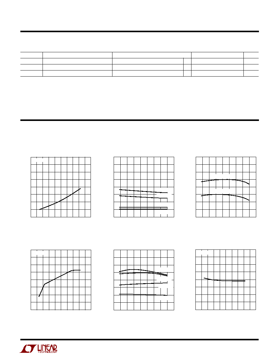
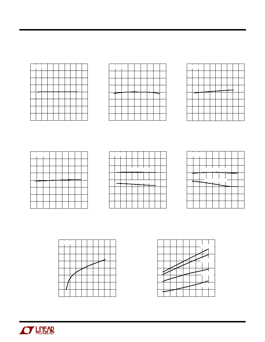
TYPICAL PERFOR A CE CHARACTERISTICS
U
W
Supply Current vs Supply Voltage
Supply Current vs Temperature
Undervoltage Lockout Threshold
vs Temperature
V
GATE
vs Supply Voltage
V
GATE
vs Temperature
I
GATEUP
vs Supply Voltage
4
LTC4210-1/LTC4210-2
421012f
75
I
GATEUP
(
µ
A)
150
25
50
0
25
50
75 100 125
TEMPERATURE (
°
C)
75
150
25
50
0
25
50
75 100 125
TEMPERATURE (
°
C)
75
150
25
50
0
25
50
75 100 125
TEMPERATURE (
°
C)
75
150
25
50
0
25
50
75 100 125
TEMPERATURE (
°
C)
75
150
25
50
0
25
50
75 100 125
TEMPERATURE (
°
C)
4210 G07
4210 G08
4210 G09
4210 G10
4210 G11
4210 G12
4210 G13
4210 G14
4210 G15
SUPPLY VOLTAGE (V)
0
V
GATE
(V)
18
16
14
12
10
8
6
4
2
V
GATE
(V)
18
16
14
12
10
8
6
4
2
20
30
40
50
60
70
80
90
100
16
4
2
6
10
14
18
8
12
20
T
A
= 25
°
C
I
TIMERUP
(
µ
A)
0
1
2
3
4
5
6
7
8
9
10
V
CC
= 15V
V
CC
= 15V
V
CC
= 12V
V
CC
= 5V
V
CC
= 3V
V
CC
= 3V
V
CC
= 5V
V
CC
= 12V
SUPPLY VOLTAGE (V)
0
I
TIMERUP
(
µ
A)
0
1
2
3
4
5
6
7
8
9
10
16
4
2
6
10
14
18
8
12
20
T
A
= 25
°
C
SUPPLY VOLTAGE (V)
0
I
TIMERDN
(
µ
A)
3.0
2.8
2.6
2.4
2.2
2.0
1.8
1.6
1.4
1.2
1.0
16
4
2
6
10
14
18
8
12
20
T
A
= 25
°
C
SUPPLY VOLTAGE (V)
0
I
TIMERUP
(
µ
A)
20
30
40
50
60
70
80
90
100
I
TIMERUP
(
µ
A)
16
4
2
6
10
14
18
8
12
20
T
A
= 25
°
C
I
TIMERDN
(
µ
A)
3.0
2.8
2.6
2.4
2.2
2.0
1.8
1.6
1.4
1.2
1.0
V
CC
= 5V
V
CC
= 5V
V
CC
= 5V
8.0
8.5
9.0
9.5
10.0
10.5
11.0
11.5
12.0
TYPICAL PERFOR A CE CHARACTERISTICS
U
W
I
TIMERUP
(In Initial Cycle)
vs Supply Voltage
I
TIMERUP
(During Circuit Breaker
Delay) vs Supply Voltage
I
TIMERUP
(During Circuit Breaker
Delay) vs Temperature
I
TIMERDN
(In Cool-Off Cycle)
vs Supply Voltage
I
TIMERUP
(In Initial Cycle)
vs Temperature
I
TIMERDN
(In Cool-Off Cycle)
vs Temperature
I
GATEUP
vs Temperature
V
GATE
vs Supply Voltage
V
GATE
vs Temperature
5
LTC4210-1/LTC4210-2
421012f
4210 G16
SUPPLY VOLTAGE (V)
0
TIMER HIGH THRESHOLD (V)
1.38
1.36
1.34
1.32
1.30
1.28
1.26
1.24
1.22
1.38
1.36
1.34
1.32
1.30
1.28
1.26
1.24
1.22
16
4
2
6
10
14
18
8
12
20
T
A
= 25
°
C
4210 G20
SUPPLY VOLTAGE (V)
0
ON PIN THRESHOLD (V)
1.45
1.40
1.35
1.30
1.25
1.20
1.15
1.10
1.05
16
4
2
6
10
14
18
8
12
20
T
A
= 25
°
C
4210 G22
SUPPLY VOLTAGE (V)
0
16
4
2
6
10
14
18
8
12
20
T
A
= 25
°
C
4210 G18
SUPPLY VOLTAGE (V)
0
TIMER LOW THRESHOLD (V)
0.24
0.23
0.22
0.21
0.20
0.19
0.18
0.17
0.16
TIMER LOW THRESHOLD (V)
0.24
0.23
0.22
0.21
0.20
0.19
0.18
0.17
0.16
16
4
2
6
10
14
18
8
12
20
T
A
= 25
°
C
75
150
25
50
0
25
50
75 100 125
TEMPERATURE (
°
C)
4210 G17
75
150
25
50
0
25
50
75 100 125
TEMPERATURE (
°
C)
4210 G21
TIMER HIGH THRESHOLD (V)
V
CC
= 5V
75
150
25
50
0
25
50
75 100 125
TEMPERATURE (
°
C)
4210 G19
V
CC
= 5V
V
CC
= 5V
HIGH THRESHOLD
LOW THRESHOLD
ON PIN THRESHOLD (V)
1.45
1.40
1.35
1.30
1.25
1.20
1.15
1.10
1.05
75
150
25
50
0
25
50
75 100 125
TEMPERATURE (
°
C)
4210 G23
t
OFF,ONLOW
(
µ
s)
80
70
60
50
40
30
20
10
0
t
OFF,ONLOW
(
µ
s)
80
70
60
50
40
30
20
10
0
HIGH THRESHOLD
LOW THRESHOLD
V
CC
= 15V
V
CC
= 12V
V
CC
= 5V
V
CC
= 3V
TYPICAL PERFOR A CE CHARACTERISTICS
U
W
TIMER Low Threshold
vs Temperature
ON Pin Threshold
vs Temperature
t
OFF(ONLOW)
vs Supply Voltage
ON Pin Threshold
vs Supply Voltage
t
OFF(ONLOW)
vs Temperature
TIMER High Threshold
vs Supply Voltage
TIMER High Threshold
vs Temperature
TIMER Low Threshold
vs Supply Voltage