 | –≠–ª–µ–∫—Ç—Ä–æ–Ω–Ω—ã–π –∫–æ–º–ø–æ–Ω–µ–Ω—Ç: LTC490IN8 | –°–∫–∞—á–∞—Ç—å:  PDF PDF  ZIP ZIP |

1
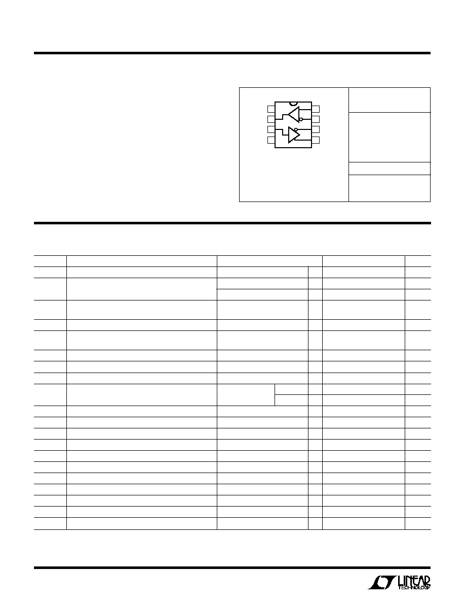
LTC490
Differential Driver and
Receiver Pair
D
U
ESCRIPTIO
S
FEATURE
s
Low Power: I
CC
= 300
µ
A Typical
s
Designed for RS485 or RS422 Applications
s
Single 5V Supply
s
≠ 7V to 12V Bus Common-Mode Range
Permits
±
7V Ground Difference Between Devices
on the Bus
s
Thermal Shutdown Protection
s
Power-Up/Down Glitch-Free Driver Outputs Permit
Live Insertion or Removal of Package
s
Driver Maintains High Impedance with the
Power Off
s
Combined Impedance of a Driver Output and
Receiver Allows up to 32 Transceivers on the Bus
s
70mV Typical Input Hysteresis
s
28ns Typical Driver Propagation Delays with
5ns Skew
s
Pin Compatible with the SN75179
The LTC490 is a low power differential bus/line transceiver
designed for multipoint data transmission standard RS485
applications with extended common-mode range (12V to
≠7V). It also meets the requirements of RS422.
The CMOS design offers significant power savings over its
bipolar counterpart without sacrificing ruggedness against
overload or ESD damage.
Excessive power dissipation caused by bus contention or
faults is prevented by a thermal shutdown circuit which
forces the driver outputs into a high impedance state. The
receiver has a fail safe feature which guarantees a high
output state when the inputs are left open.
Both AC and DC specifications are guaranteed from 0
∞
C to
70
∞
C and 4.75V to 5.25V supply voltage range.
U
S
A
O
PPLICATI
s
Low Power RS485/RS422 Transceiver
s
Level Translator
U
A
O
PPLICATI
TYPICAL
LTC490 ∑ TA01
120
120
120
120
4000 FT BELDEN 9841
4000 FT BELDEN 9841
RECEIVER
LTC490
DRIVER
RECEIVER
LTC490
DRIVER
R
D
R
D
3
2
7
8
6
5
LTC490
2
(Note 1)
Supply Voltage (V
CC
) ............................................... 12V
Driver Input Currents ........................... ≠ 25mA to 25mA
Driver Input Voltages ....................... ≠0.5V to V
CC
+0.5V
Driver Output Voltages ..........................................
±
14V
Receiver Input Voltages .........................................
±
14V
Receiver Output Voltages ................ ≠0.5V to V
CC
+0.5V
Operating Temperature Range
LTC490C................................................. 0
∞
C to 70
∞
C
LTC490I............................................. ≠ 40
∞
C to 85
∞
C
Storage Temperature Range ................. ≠ 65
∞
C to 150
∞
C
Lead Temperature (Soldering, 10 sec).................. 300
∞
C
A
U
G
W
A
W
U
W
A
R
BSOLUTE
XI
TI
S
W
U
U
PACKAGE/ORDER I FOR ATIO
T
JMAX
= 125
∞
C,
JA
= 100
∞
C/ W (N8)
T
JMAX
= 150
∞
C,
JA
= 150
∞
C/ W (S8)
N8 PACKAGE
8-LEAD PLASTIC DIP
S8 PACKAGE
8-LEAD PLASTIC SOIC
1
2
3
4
8
7
6
5
TOP VIEW
V
CC
R
D
GND
A
B
Z
Y
R
D
ORDER PART
NUMBER
S8 PART MARKING
LTC490CN8
LTC490CS8
LTC490IN8
LTC490IS8
490
490I
ELECTRICAL C
C
HARA TERISTICS
C
D
V
CC
= 5V
±
5%
SYMBOL
PARAMETER
CONDITIONS
MIN
TYP
MAX
UNITS
V
OD1
Differential Driver Output Voltage (Unloaded)
I
O
= 0
q
5
V
V
OD2
Differential Driver Output Voltage (with Load)
R = 50
(RS422)
q
2
V
R = 27
(RS485) (Figure 1)
q
1.5
5
V
V
OD
Change in Magnitude of Driver Differential Output
R = 27
or R = 50
(Figure 1)
q
0.2
V
Voltage for Complementary Output States
V
OC
Driver Common-Mode Output Voltage
R = 27
or R = 50
(Figure 1)
q
3
V
V
OC
Change in Magnitude of Driver Common Mode
R = 27
or R = 50
(Figure 1)
q
0.2
V
Output Voltage for Complementary Output States
V
IH
Input High Voltage (D)
q
2.0
V
V
IL
Input Low Voltage (D)
q
0.8
V
l
IN1
Input Current (D)
q
±
2
µ
A
l
IN2
Input Current (A, B)
V
CC
= 0V or 5.25V V
IN
= 12V
q
1
mA
V
IN
= ≠ 7V
q
≠ 0.8
mA
V
TH
Differential Input Threshold Voltage for Receiver
≠ 7V
V
CM
12V
q
≠ 0.2
0.2
V
V
TH
Receiver Input Hysteresis
V
CM
= 0V
q
70
mV
V
OH
Receiver Output High Voltage
I
O
= ≠4mA, V
ID
= 0.2V
q
3.5
V
V
OL
Receiver Output Low Voltage
I
O
= 4mA, V
ID
= ≠ 0.2V
q
0.4
V
I
OZR
Three-State Output Current at Receiver
V
CC
= Max 0.4V
V
O
2.4V
q
±
1
µ
A
I
CC
Supply Current
No Load; D = GND or V
CC
q
300
500
µ
A
R
IN
Receiver Input Resistance
≠ 7V
V
O
12V
q
12
k
I
OSD1
Driver Short-Circuit Current, V
OUT
= High
V
O
= ≠ 7V
q
100
250
mA
I
OSD2
Driver Short-Circuit Current, V
OUT
= Low
V
O
= 12V
q
100
250
mA
I
OSR
Receiver Short-Circuit Current
0V
V
O
V
CC
q
7
85
mA
I
OZ
Driver Three-State Output Current
V
O
= ≠ 7V to 12V
q
±
2
±
200
µ
A
Consult factory for Military grade parts.

3
LTC490
V
CC
= 5V
±
5%
The
q
denotes specifications which apply over the full operating
temperature range.
Note 1: Absolute maximum ratings are those beyond which the safety of
the device cannot be guaranteed.
Note 2: All currents into device pins are positive; all currents out of device
pins are negative. All voltages are referenced to device ground unless
otherwise specified.
Note 3: All typicals are given for V
CC
= 5V and Temperature = 25
∞
C.
S
U
G C
C
HARA TERISTICS
WITCHI
SYMBOL
PARAMETER
CONDITIONS
MIN
TYP
MAX
UNITS
t
PLH
Driver Input to Output
R
DIFF
= 54
, C
L1
= C
L2
= 100pF (Figures 2, 3)
q
10
30
50
ns
t
PHL
Driver Input to Output
R
DIFF
= 54
, C
L1
= C
L2
= 100pF (Figures 2, 3)
q
10
30
50
ns
t
SKEW
Driver Output to Output
R
DIFF
= 54
, C
L1
= C
L2
= 100pF (Figures 2, 3)
q
5
ns
t
r
, t
f
Driver Rise or Fall Time
R
DIFF
= 54
, C
L1
= C
L2
= 100pF (Figures 2, 3)
q
5
5
25
ns
t
PLH
Receiver Input to Output
R
DIFF
= 54
, C
L1
= C
L2
= 100pF (Figures 2, 4)
q
40
70
150
ns
t
PHL
Receiver Input to Output
R
DIFF
= 54
, C
L1
= C
L2
= 100pF (Figures 2, 4)
q
40
70
150
ns
t
SKD
t
PLH
≠ t
PHL
Differential Receiver Skew
R
DIFF
= 54
, C
L1
= C
L2
= 100pF (Figures 2, 4)
q
13
ns
C
C
HARA TERISTICS
U
W
A
TYPICAL PERFOR
CE
Driver Output High Voltage vs
Driver Differential Output Voltage
Driver Output Low Voltage vs
Output Current
vs Output Current
Output Current
OUTPUT VOLTAGE (V)
0
OUTPUT CURRENT (mA)
0
≠24
≠ 48
≠72
≠96
1
2
3
4
LTC490 ∑ TPC01
T
A
= 25∞C
OUTPUT VOLTAGE (V)
0
OUTPUT CURRENT (mA)
0
16
32
48
64
1
2
3
4
LTC490 ∑ TPC02
T
A
= 25∞C
OUTPUT VOLTAGE (V)
0
OUTPUT CURRENT (mA)
0
20
40
60
80
1
2
3
4
LTC490 ∑ TPC03
T
A
= 25∞C
TEMPERATURE (∞C )
≠50
SUPPLY CURRENT (
µ
A)
310
320
330
340
350
0
50
100
LTC490 ∑ TPC06
TEMPERATURE (∞C )
≠50
INPUT THRESHOLD VOLTAGE (V)
1.55
1.57
1.59
1.61
1.63
0
50
100
LTC490 ∑ TPC04
TTL Input Threshold vs
Temperature
Driver Skew vs Temperature
Supply Current vs Temperature
TEMPERATURE (∞C )
≠50
TIME (ns)
5
4
3
2
1
0
50
100
LTC490 ∑ TPC05

LTC490
4
C
C
HARA TERISTICS
U
W
A
TYPICAL PERFOR
CE
PI
U
FU
U
C
U
S
O
TI
V
CC
(Pin 1): Positive Supply; 4.75V
V
CC
5.25V.
R (Pin 2): Receiver Output. If A > B by 200mV, R will be
high. If A < B by 200mV, then R will be low.
D (Pin 3): Driver Input. A low on D forces the driver outputs
A low and B high. A high on D will force A high and B low.
GND (Pin 4): Ground Connection.
Y (Pin 5): Driver Output.
Z (Pin 6): Driver Output.
B (Pin 7): Receiver Input.
A (Pin 8): Receiver Input.
Driver Differential Output Voltage
Receiver
t
PLH
-t
PHL
vs
Receiver Output Low Voltage vs
vs Temperature
Temperature
Temperature
TEMPERATURE (∞C )
≠50
DIFFERENTIAL VOLTAGE (V)
1.5
1.7
1.9
2.1
2.3
0
50
100
LTC490 ∑ TPC07
R
O
= 54
TEMPERATURE (∞C )
≠50
TIME (ns)
7
6
5
4
3
0
50
100
LTC490 ∑ TPC08
TEMPERATURE (∞C )
≠50
OUTPUT VOLTAGE (V)
0
0.2
0.4
0.6
0.8
0
50
100
LTC490 ∑ TPC09
I = 8mA
TEST CIRCUITS
Figure 1. Driver DC Test Load
LTC490 ∑ TA03
DRIVER
D
Y
Z
RECEIVER
R
DIFF
A
B
15pF
C
L1
C
L2
R
Figure 2. Driver/Receiver Timing Test Circuit
LTC490 ∑ TA02
Y
Z
R
R
V
OD2
V
OC
5
LTC490
Figure 4. Receiver Propagation Delays
Figure 3. Driver Propagation Delays
TI
W
E WAVEFOR
S
U
G
WITCHI
W
S
U
S
A
O
PPLICATI
W
U
U
I FOR ATIO
Typical Application
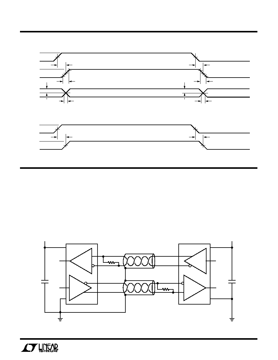
A typical connection of the LTC490 is shown in Figure 5.
Two twisted-pair wires connect two driver/receiver pairs
for full duplex data transmission. Note that the driver and
receiver outputs are always enabled. If the outputs must be
disabled, use the LTC491.
There are no restrictions on where the chips are con-
nected, and it isn't necessary to have the chips connected
at the ends of the wire. However, the wires must be
terminated only at the ends with a resistor equal to their
characteristic impedance, typically 120
. Because only
Figure 5. Typical Connection
LTC490 ∑ TA06
120
120
SHIELD
LTC490
DRIVER
RECEIVER
LTC490
DRIVER
DX
RX
DX
RX
2
3
5
6
7
8
RECEIVER
+
0.01
µ
F
1
4
5V
SHIELD
8
7
6
5
+
0.01
µ
F
5V
4
2
3
1
V
OL
LTC490 ∑ TA05
A-B
V
OD2
0V
t
PLH
0V
OUTPUT
V
OH
1.5V
f = 1MHz ; t
r
10ns : t
f
10ns
t
PHL
≠V
OD2
1.5V
INPUT
R
≠V
O
LTC490 ∑ TA04
D
3V
0V
1.5V
t
PLH
1.5V
V
DIFF
= V(Y) ≠ V(Z)
V
O
80%
20%
50%
10%
Z
Y
t
SKEW
t
r
f = 1MHz : t
r
10ns : t
f
10ns
90%
50%
t
PHL
t
f
V
O
t
SKEW
1/2 V
O
1/2 V
O