 | –≠–ª–µ–∫—Ç—Ä–æ–Ω–Ω—ã–π –∫–æ–º–ø–æ–Ω–µ–Ω—Ç: LTC660CS8 | –°–∫–∞—á–∞—Ç—å:  PDF PDF  ZIP ZIP |
1
LTC660
100mA CMOS
Voltage Converter
TYPICAL APPLICATIO
N
U
s
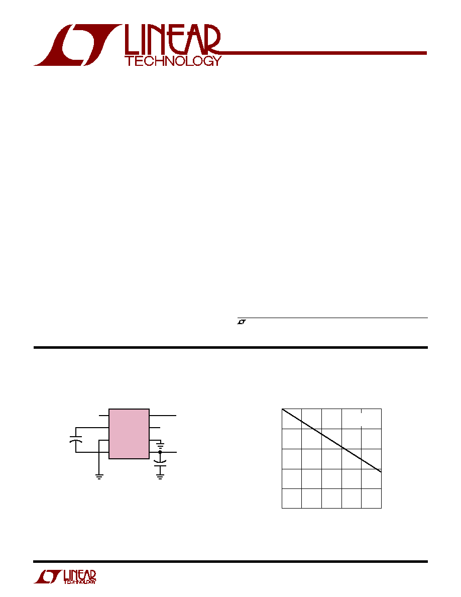
Simple Conversion of 5V to ≠ 5V Supply
s
Output Drive: 100mA
s
R
OUT
: 6.5
(0.65V Loss at 100mA)
s
BOOST Pin (Pin 1) for Higher Switching Frequency
s
Inverting and Doubling Modes
s
Minimum Open Circuit Voltage Conversion
Efficiency: 99%
s
Typical Power Conversion Efficiency
with a 100mA Load: 88%
s
Easy to Use
The LTC
Æ
660 is a monolithic CMOS switched-capacitor
voltage converter. It performs supply voltage conversion
from positive to negative from an input range of 1.5V to
5.5V, resulting in complementary output voltages of
≠ 1.5V to ≠ 5.5V. It also performs a doubling at an input
voltage range of 2.5V to 5.5V, resulting in a doubled
output voltage of 5V to 11V. Only two external capacitors
are needed for the charge pump and charge reservoir
functions.
The converter has an internal oscillator that can be
overdriven by an external clock or slowed down when
connected to a capacitor. The oscillator runs at a 10kHz
frequency when unloaded. A higher frequency outside the
audio band can also be obtained if the BOOST pin is tied
to V
+
.
The LTC660 contains an internal oscillator, divide-by-two,
voltage level shifter and four power MOSFETs.
s
Conversion of 5V to
±
5V Supplies
s
Inexpensive Negative Supplies
s
Data Acquisition Systems
s
High Current Upgrade to LTC1044 or LTC7660
FEATURES
DESCRIPTIO
N
U
APPLICATIO
N
S
U
Output Voltage vs
Load Current for V
+
= 5V
LOAD CURRENT (mA)
0
OUTPUT VOLTAGE (V)
≠5.0
≠4.8
≠4.6
≠4.4
≠4.2
≠4.0
80
660 TA02
20
40
60
100
T
A
= 25
∞
C
R
OUT
= 6.5
, LTC and LT are registered trademarks of Linear Technology Corporation.
Generating ≠ 5V from 5V
1
2
3
4
8
7
6
5
BOOST
CAP
+
GND
CAP
≠
C2
150
µ
F
660 TA01
C1
150
µ
F
≠5V
OUTPUT
5V INPUT
LTC660
V
+
OSC
LV
V
OUT
+
+

2
LTC660
ABSOLUTE
M
AXI
M
U
M
RATINGS
W
W
W
U
PACKAGE/ORDER I
N
FOR
M
ATIO
N
W
U
U
Supply Voltage (V
+
) .................................................. 6V
Input Voltage on Pins 1, 6, 7
(Note 2) ............................ ≠ 0.3V < V
IN
< (V
+
+ 0.3V)
Output Short-Circuit Duration to GND
(Note 5) ............................................................. 1 sec
Power Dissipation .............................................. 500mW
Operating Temperature Range .................... 0
∞
C to 70
∞
C
Storage Temperature Range ................. ≠ 65
∞
C to 150
∞
C
Lead Temperature (Soldering, 10 sec).................. 300
∞
C
(Note 1)
1
2
3
4
8
7
6
5
TOP VIEW
BOOST
CAP
+
GND
CAP
≠
V
+
OSC
LV
V
OUT
N8 PACKAGE
8-LEAD PLASTIC DIP
S8 PACKAGE
8-LEAD PLASTIC SOIC
660
T
JMAX
= 100
∞
C,
JA
= 100
∞
C/W (N)
T
JMAX
= 100
∞
C,
JA
= 150
∞
C/W (S)
Consult Factory for Industrial and Military grade parts.
LTC660CN8
LTC660CS8
ORDER PART
NUMBER
S8 PART MARKING
SYMBOL PARAMETER
CONDITIONS
MIN
TYP
MAX
UNITS
Supply Voltage
R
L
= 1k
Inverter, LV = Open
q
3
5.5
V
Inverter, LV = GND
q
1.5
5.5
V
Doubler, LV = V
OUT
q
2.5
5.5
V
I
S
Supply Current
No Load
Boost = Open
q
0.08
0.5
mA
Boost = V
+
q
0.23
3
mA
I
OUT
Output Current
V
OUT
More Negative Than ≠ 4V
q
100
mA
R
OUT
Output Resistance
I
L
= 100mA (Note 3)
q
6.5
10
f
OSC
Oscillator Frequency
Boost = Open
10
kHz
Boost = V
+
(Note 4)
80
kHz
Power Efficiency
R
L
= 1k Connected Between V
+
and V
OUT
q
96
98
%
R
L
= 500
Connected Between V
OUT
and GND
q
92
96
%
I
L
= 100mA to GND
88
%
Voltage Conversion Efficiency
No Load
99
99.96
%
Oscillator Sink or Source Current
Boost = Open
±
1.1
µ
A
Boost = V
+
±
5.0
µ
A
V
+
= 5V, C1
and C2
= 150
µ
F, Boost = Open, C
OSC
= 0pF, T
A
= 25
∞
C, unless otherwise noted.
ELECTRICAL CHARACTERISTICS
The
q
denotes specifications which apply over the full operating
temperature range; all other limits and typicals are at T
A
= 25
∞
C.
Note 1: Absolute Maximum Ratings are those values beyond which the life
of a device may be impaired.
Note 2: Connecting any input terminal to voltages greater than V
+
or less
than ground may cause destructive latch-up. It is recommended that no
inputs from source operating from external supplies be applied prior to
power-up of the LTC660.
Note 3: The output resistance is a combination of internal switch
resistance and external capacitor ESR. To maximize output voltage and
efficiency, keep external capacitor ESR < 0.2
.
Note 4: f
OSC
is tested with C
OSC
= 100pF to minimize the effects of test
fixture capacitance loading. The 0pF frequency is correlated to this 100pF
test point, and is intended to simulate the capacitance at Pin 7 when the
device is plugged into a test socket and no external capacitor is used.
Note 5: OUT may be shorted to GND for 1 sec without damage, but
shorting OUT to V
+
may damage the device and should be avoided. Also,
for temperatures above 85
∞
C, OUT must not be shorted to GND or V
+
,
even instantaneously, or device damage may result.

3
LTC660
TYPICAL PERFOR
M
A
N
CE CHARACTERISTICS
U
W
(Using Test Circuit in Figure 1)
Output Voltage and Efficiency
vs Load Current, V
+
= 5V
LOAD CURRENT (mA)
0
OUTPUT VOLTAGE (V)
EFFICIENCY (%)
≠3.8
≠3.4
≠3.0
80
LTC660 ∑ TPC06
≠4.2
≠4.6
≠5.0
84
92
100
76
68
80
88
96
72
64
60
20
40
60
10
90
30
50
70
100
LTC660
EFFICIENCY
LTC660
OUTPUT VOLTAGE
T
A
= 25
∞
C
BOOST = OPEN
OSCILLATOR FREQUENCY (kHz)
0.1
40
OUTPUT RESISTANCE (
)
50
60
70
80
1
10
100
LTC660 ∑ TPC03
30
20
10
0
90
100
C1 = C2 = 22
µ
F
C1 = C2 = 150
µ
F
C1 = C2 = 1500
µ
F
T
A
= 25
∞
C
V
+
= 5V
BOOST = OPEN
Output Resistance
vs Oscillator Frequency
LOAD CURRENT (mA)
0
EFFICIENCY (%)
90
100
80
LTC660 ∑ TPC07
80
70
85
95
75
65
60
20
40
60
10
90
30
50
70
100
V
+
= 5.5V
T
A
= 25
∞
C
BOOST = OPEN
V
+
= 4.5V
V
+
= 3.5V
V
+
= 2.5V
V
+
= 1.5V
Efficiency vs Load Current
SUPPLY VOLTAGE (V)
0
0
OUTPUT RESISTANCE (
)
2
6
8
10
2
18
LTC690 ∑ TPC04
4
1
3
4
5
6
12
14
16
T
A
= 25
∞
C
BOOST = OPEN
Output Resistance
vs Supply Voltage
TEMPERATURE (
∞
C)
≠60
OUTPUT RESISTANCE (
)
15
20
25
100
LTC660 ∑ TPC05
10
5
0
≠20
20
60
140
80
≠40
0
40
120
V
+
= 1.5V
BOOST = OPEN
V
+
= 3V
V
+
= 5V
Output Resistance vs Temperature
Output Voltage Drop
vs Load Current
LOAD CURRENT (mA)
0
OUTPUT VOLTAGE DROP FROM
SUPPLY VOLTAGE (V)
0.8
1.0
80
LTC660 ∑ TPC09
0.6
0.4
0.7
0.9
0.5
0.3
0.2
0.1
0
20
40
60
10
90
30
50
70
100
V
+
= 5.5V
T
A
= 25
∞
C
BOOST = OPEN
V
+
= 2.5V
V
+
= 1.5V
V
+
= 3.5V
V
+
= 4.5V
Efficiency vs Load Current
LOAD CURRENT (mA)
0
EFFICIENCY (%)
90
100
80
LTC660 ∑ TPC08
80
70
85
95
75
65
60
20
40
60
10
90
30
50
70
100
V
+
= 5.5V
T
A
= 25
∞
C
BOOST = V
+
V
+
= 3.5V
V
+
= 2.5V
V
+
= 1.5V
V
+
= 4.5V
SUPPLY VOLTAGE (V)
1.5
0
SUPPLY CURRENT (
µ
A)
50
100
150
200
2.5
3.5
4.5
5.5
LTC660 ∑ G01
250
300
2
3
4
5
BOOST = V
+
BOOST = OPEN
T
A
= 25
∞
C
Supply Current vs Supply Voltage
OSCILLATOR FREQUENCY (kHz)
10
100
SUPPLY CURRENT (
µ
A)
1000
0.01
1
10
1000
LTC660 ∑ G02
1
0.1
100
T
A
= 25
∞
C
V
+
= 5V
Supply Current
vs Oscillator Frequency

4
LTC660
TYPICAL PERFOR
M
A
N
CE CHARACTERISTICS
U
W
(Using Test Circuit in Figure 1)
Oscillator Frequency
vs Temperature
TEMPERATURE (
∞
C)
0
OSCILLATOR FREQUENCY (kHz)
4
8
12
2
6
10
≠20
20
60
100
LTC660 ∑ TPC15
140
≠40
≠60
0
40
80
120
V
+
= 5V
BOOST = OPEN
OSC = OPEN
LOAD CURRENT (mA)
0
OUTPUT VOLTAGE DROP FROM
SUPPLY VOLTAGE (V)
0.8
1.0
80
LTC660 ∑ TPC10
0.6
0.4
0.7
0.9
0.5
0.3
0.2
0.1
0
20
40
60
10
90
30
50
70
100
V
+
= 5.5V
T
A
= 25
∞
C
BOOST = V
+
V
+
= 2.5V
V
+
= 1.5V
V
+
= 3.5V
V
+
= 4.5V
Output Voltage Drop
vs Load Current
Output Voltage
vs Oscillator Frequency
OSCILLATOR FREQUENCY (kHz)
0.1
≠2.5
OUTPUT VOLTAGE (V)
≠4.0
≠4.5
≠5.0
1
10
100
LTC660 ∑ TPC11
≠3.5
≠3.0
T
A
=25
∞
C
V
+
= 5V
BOOST = OPEN
I
L
= 1mA
I
L
= 10mA
I
L
= 80mA
Efficiency vs Oscillator Frequency
OSCILLATOR FREQUENCY (kHz)
0.1
70
EFFICIENCY (%)
75
80
85
90
1
10
100
LTC660 ∑ TPC12
65
60
55
50
95
100
T
A
= 25
∞
C
V
+
= 5V
BOOST = OPEN
I
L
= 10mA
I
L
= 80mA
I
L
= 1mA
Oscillator Frequency
vs Supply Voltage
SUPPLY VOLTAGE (V)
0
OSCILLATOR FREQUENCY (kHz)
4
8
12
2
6
10
1.0
2.5
3.5
4.5
LTC660 ∑ TPC13
5.5
0.5
0
1.5 2.0
3.0
4.0
5.0
T
A
= 25
∞
C
BOOST = OPEN
OSC = OPEN
Oscillator Frequency
vs Supply Voltage
SUPPLY VOLTAGE (V)
0
OSCILLATOR FREQUENCY (kHz)
60
50
40
30
20
80
100
10
70
90
1.0
2.5
3.5
4.5
LTC660 ∑ TPC14
5.5
0.5
0
1.5 2.0
3.0
4.0
5.0
T
A
= 25
∞
C
BOOST = V
+
OSC = OPEN
Oscillator Frequency
vs Temperature
TEMPERATURE (
∞
C)
≠60
OSCILLATOR FREQUENCY (kHz)
60
80
100
100
LTC660 ∑ TPC16
40
20
10
70
90
50
30
0
≠20
20
60
≠40
120
0
40
80
140
V
+
= 5V
BOOST = V
+
OSC = OPEN
Oscillator Frequency
vs External Capacitance
CAPACITANCE (pF)
00.1
OSCILLATOR FREQUENCY (kHz)
1
100
1000
100
10
1
10000
LTC660 ∑ TPC17
0.1
10
BOOST = V
+
BOOST = OPEN

5
LTC660
PIN
NAME
INVERTER
DOUBLER
1
BOOST
Internal Oscillator Frequency Control Pin.
Same
BOOST = Open, f
OSC
= 10kHz typ;
BOOST = V
+
, f
OSC
= 80kHz typ; when OSC is driven
externally BOOST has no effect.
2
CAP
+
Positive Terminal for Charge Pump Capacitor
Same
3
GND
Power Supply Ground Input
Positive Voltage Input
4
CAP
≠
Negative Terminal for Charge Pump Capacitor
Same
5
V
OUT
Negative Voltage Output
Power Supply Ground Input
6
LV
Tie LV to GND when the input voltage is less than 3V.
LV must be tied to V
OUT
for all input voltages.
LV may be connected to GND or left open for input
voltages above 3V. Connect LV to GND when
overdriving OSC.
7
OSC
An external capacitor can be connected to this pin to
Same except standard logic levels will not be able to
slow the oscillator frequency. Keep stray capacitance
overdrive OSC pin.
to a minimum. An external oscillator can be applied
to this pin to overdrive the internal oscillator.
8
V
+
Positive Voltage Input
Positive Voltage Output
PI
N
FU
N
CTIO
N
S
U
U
U
TEST CIRCUIT
V
+
LTC660
1
2
3
4
8
7
6
5
C1
150
µ
F
V
+
5V
EXTERNAL
OSCILLATOR
C
OSC
V
OUT
LTC660 ∑ F01
R
L
I
S
I
L
C1
150
µ
F
+
+
Figure 1. Test Circuit

6
LTC660
APPLICATIO
N
S I
N
FOR
M
ATIO
N
W
U
U
U
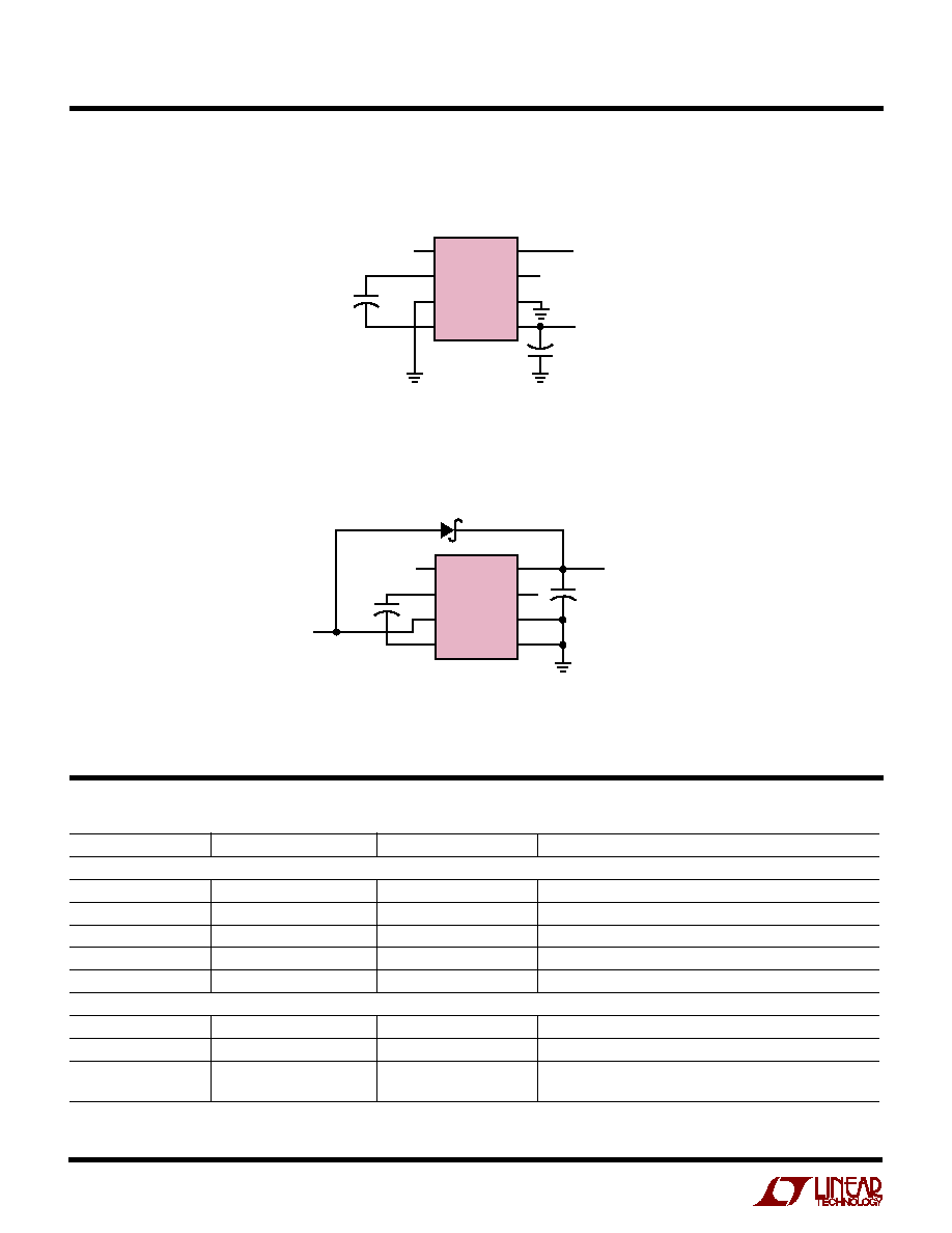
Theory of Operation
To understand the theory of operation for the LTC660, a
review of a basic switched-capacitor building block is
helpful. In Figure 2, when the switch is in the left position,
capacitor C1 will charge to voltage V1. The total charge on
C1 will be q1 = C1V1. The switch then moves to the right,
discharging C1 to voltage V2. After this discharging time,
the charge on C1 is q2 = C1V2. Note that charge has been
transferred from the source V1 to the output V2. The
amount of charge transferred is:
q = q1 ≠ q2 = C1 (V1 ≠ V2)
If the switch is cycled "f" times per second, the charge
transfer per unit time (i.e., current) is:
I = f ∑
q = f ∑ C1 (V1 ≠ V2)
Rewriting in terms of voltage and impedance equivalence,
I
V
V
fC
V
V
R
EQUIV
=
-
=
-
1
2
1
1
1
2
/
A new variable R
EQUIV
has been defined such that
R
EQUIV
= 1/fC1. Thus, the equivalent circuit for the switched-
capacitor network is as shown in Figure 3.
Figure 4 shows that the LTC660 has the same switching
action as the basic switched-capacitor building block.
Figure 2. Switched-Capacitor Building Block
Figure 3. Switched-Capacitor Equivalent Circuit
LTC660 ∑ F04
CAP
+
(2)
CAP
≠
(4)
GND
(3)
V
OUT
(5)
V
+
(8)
LV
(6)
4.5
◊
(1)
OSC
(7)
OSC
+2
CLOSED WHEN
V
+
> 3.0V
C1
C2
BOOST
SW1
SW2
+
+
Figure 4. LTC660 Switched-Capacitor Voltage Converter
Block Diagram
This simplified circuit does not include finite on-resistance
of the switches and output voltage ripple, however, it does
give an intuitive feel for how the device works. For ex-
ample, if you examine power conversion efficiency as a
function of frequency this simple theory will explain how
the LTC660 behaves. The loss and hence the efficiency is
set by the output impedance. As frequency is decreased,
the output impedance will eventually be dominated by the
1/fC1 term and voltage losses will rise decreasing the
efficiency. As the frequency increases the quiescent cur-
rent increases. At high frequency this current loss be-
comes significant and the power efficiency starts to de-
crease.
The LTC660 oscillator frequency is designed to run where
the voltage loss is a minimum. With the external 150
µ
F
capacitors the effective output impedance is determined
by the internal switch resistances and the capacitor ESRs.
LV (Pin 6)
The internal logic of the LTC660 runs between V
+
and LV
(Pin 6). For V
+
3V, an internal switch shorts LV to ground
(Pin 3). For V
+
< 3V, the LV pin should be tied to ground.
For V
+
3V, the LV pin can be tied to ground or left floating.
OSC (Pin 7) and BOOST (Pin 1)
The switching frequency can be raised, lowered or driven
from an external source. Figure 5 shows a functional
diagram of the oscillator circuit.
C1
C2
V2
660 F02
V1
R
L
C2
V2
660 F03
V1
R
L
R
EQUIV
R
EQUIV
=
1
fC1

7
LTC660
APPLICATIO
N
S I
N
FOR
M
ATIO
N
W
U
U
U
Figure 5. Oscillator
OSC
(7)
LTC660 ∑ F05
LV
(6)
BOOST
(1)
18pF
I
I
7.0I
7.0I
V
+
SCHMITT
TRIGGER
Figure 6. External Clocking
Capacitor Selection
While the exact values of C1 and C2 are noncritical, good
quality, low ESR capacitors are necessary to minimize
voltage losses at high currents. For C1 the effect of the ESR
of the capacitor will be multiplied by four, due to the fact
the switch currents are approximately two times higher
than the output current and losses will occur on both the
charge and discharge cycle. This means using a capacitor
with 1
of ESR for C1 will have the same effect as
increasing the output impedance of the LTC660 by 4
.
This represents a significant increase in the voltage losses.
For C2 the effect of ESR is less dramatic. A C2 with 1
of
ESR will increase the output impedance by 1
. The size
of C2 and the load current will determine the output
voltage ripple. It is alternately charged and discharged at
a current approximately equal to the output current. This
will cause a step function to occur in the output voltage at
the switch transitions. For example, for a switching fre-
quency of 5kHz (one-half the nominal 10kHz oscillator
frequency) and C2 = 150
µ
F with an ESR of 0.2
, ripple is
approximately 90mV with a 100mA load current.
By connecting the BOOST pin (Pin 1) to V
+
, the charge and
discharge current is increased and, hence, the frequency
is increased by approximately four and a half times.
Increasing the frequency will decrease output impedance
and ripple for high load currents.
Loading Pin 7 with more capacitance will lower the fre-
quency. Using the BOOST (Pin 1) in conjunction with
external capacitance on Pin 7 allows user selection of the
frequency over a wide range.
Driving the LTC660 from an external frequency source can
be easily achieved by driving Pin 7 and leaving the BOOST
pin open, as shown in Figure 6. The output current from
Pin 7 is small, typically 1.1
µ
A to 8
µ
A, so a logic gate is
capable of driving this current. (A CMOS logic gate can be
used to drive the OSC pin.) For 5V applications, a TTL logic
gate can be used by simply adding an external pull-up
resistor (see Figure 6).
8
7
6
5
4
3
2
1
C1
C2
≠(V
+
)
V
+
100k
REQUIRED FOR TTL LOGIC
LTC660 ∑ F06
NC
OSC INPUT
LTC660
+
+

8
LTC660
TYPICAL APPLICATIO
N
S
N
U
Voltage Doubling
Figure 8 shows the LTC660 operating in the voltage
doubling mode. The external Schottky (1N5817) diode is
for start-up only. The output voltage is 2 ∑ V
IN
without a
load. The diode has no effect on the output voltage.
1
2
3
4
8
7
6
5
BOOST
CAP
+
GND
CAP
≠
LTC660 ∑ F08
C1
150
µ
F
V
OUT
= 2V
IN
V
IN
2.5V
TO 5.5V
LTC660
1N5817*
V
+
OSC
LV
V
OUT
C2
150
µ
F
* SCHOTTKY DIODE IS FOR START-UP ONLY
+
+
Figure 8. Voltage Doubler
Negative Voltage Converter
Figure 7 shows a typical connection which will provide a
negative supply from an available positive supply. This
circuit operates over full temperature and power supply
ranges without the need of any external diodes. The LV pin
(Pin 6) is shown grounded, but for V
+
3V, it may be
floated, since LV is internally switched to ground (Pin 3)
for V
+
3V.
The output voltage (Pin 5) characteristics of the circuit are
those of a nearly ideal voltage source in series with a 6.5
resistor. The 6.5
output impedance is composed of two
terms: 1) the equivalent switched-capacitor resistance
(see Theory of Operation), and 2) a term related to the on-
resistance of the MOS switches.
At an oscillator frequency of 10kHz and C1 = 150
µ
F, the
first term is:
R
=
1
f
/2
EQUIV
OSC
( )
=
=
C1
1
5 10
150 10
1 3
3
6
∑
∑
∑
.
≠
.
Notice that the equation for R
EQUIV
is not a capacitive
reactance equation (X
C
= 1/
C) and does not contain a
2
term.
The exact expression for output impedance is complex,
but the dominant effect of the capacitor is clearly shown on
the typical curves of output impedance and power effi-
ciency versus frequency. For C1 = C2 = 150
µ
F, the output
impedance goes from 6.5
at f
OSC
= 10kHz to 110
at
f
OSC
= 100Hz. As the 1/fC term becomes large compared
to the switch on-resistance term, the output resistance is
determined by 1/fC only.
Ultraprecision Voltage Divider
An ultraprecision voltage divider is shown in Figure 9. To
achieve the 0.002% accuracy indicated, the load current
should be kept below 100nA. However, with a slight loss
in accuracy, the load current can be increased.
1
2
3
4
8
7
6
5
BOOST
CAP
+
GND
CAP
≠
C2
150
µ
F
LTC660 ∑ F07
C1
150
µ
F
V
OUT
= ≠V
IN
V
IN
1.5V TO 5.5V
LTC660
V
+
OSC
LV
V
OUT
+
+
Figure 7. Voltage Inverter
Battery Splitter
A common need in many systems is to obtain positive and
negative supplies from a single battery or single power
supply system. Where current requirements are small, the
circuit shown in Figure 10 is a simple solution. It provides
symmetrical positive or negative output voltages, both
equal to one-half the input voltage. The output voltages are
both referenced to Pin 3 (Output Common).
Figure 9. Ultraprecision Voltage Divider
8
7
6
5
4
3
2
1
C1
150
µ
F
±
0.002%
V
+
3V TO 11V
LTC660 ∑ F09
T
MIN
T
A
T
MAX
I
L
100nA
C2
150
µ
F
2
V
+
LTC660
+
+

9
LTC660
TYPICAL APPLICATIO
N
S
N
U
8
7
6
5
4
3
2
1
C1
150
µ
F
+V
B
/2 (4.5V)
LTC1046 ∑ TA10
C2
150
µ
F
OUTPUT COMMON
≠V
B
/2 (≠4.5V)
V
B
(9V)
3V
V
B
11V
LTC660
+
+
Figure 10. Battery Splitter
Paralleling for Lower Output Resistance
Additional flexibility of the LTC660 is shown in Figures 11
and 12. Figure 11 shows two LTC660s connected in
parallel to provide a lower effective output resistance. If,
however, the output resistance is dominated by 1/fC1,
increasing the capacitor size (C1) or increasing the fre-
quency will be of more benefit than the paralleling circuit
shown.
Stacking for Higher Voltage
Figure 12 makes use of "stacking" two LTC660s to provide
even higher voltages. In Figure 12, a negative voltage
doubler or tripler can be achieved depending upon how
Pin 8 of the second LTC660 is connected, as shown
schematically by the switch.
Figure 12. Stacking for High Voltage
8
7
6
5
4
3
2
1
150
µ
F
V
+
LTC660 ∑ F12
150
µ
F
150
µ
F
V
OUT
≠V
+
150
µ
F
FOR V
OUT
= ≠2V
+
FOR V
OUT
= ≠3V
+
LTC660
1
8
7
6
5
4
3
2
1
LTC660
2
+
+
+
+
8
7
6
5
4
3
2
1
C1
150
µ
F
V
+
LTC660 ∑ F11
8
7
6
5
4
3
2
1
C1
150
µ
F
C2
150
µ
F
V
OUT
= ≠V
+
1/4 CD4077
OPTIONAL SYNCHRONIZATION
CIRCUIT TO MINIMIZE RIPPLE
LTC660
LTC660
+
+
+
Figure 11. Paralleling for 200mA Load Current
10
LTC660
PACKAGE DESCRIPTIO
N
U
Dimensions in inches (millimeters) unless otherwise noted.
N8 Package
8-Lead PDIP (Narrow 0.300)
(LTC DWG # 05-08-1510)
N8 1197
0.100
±
0.010
(2.540
±
0.254)
0.065
(1.651)
TYP
0.045 ≠ 0.065
(1.143 ≠ 1.651)
0.130
±
0.005
(3.302
±
0.127)
0.020
(0.508)
MIN
0.018
±
0.003
(0.457
±
0.076)
0.125
(3.175)
MIN
1
2
3
4
8
7
6
5
0.255
±
0.015*
(6.477
±
0.381)
0.400*
(10.160)
MAX
0.009 ≠ 0.015
(0.229 ≠ 0.381)
0.300 ≠ 0.325
(7.620 ≠ 8.255)
0.325
+0.035
≠0.015
+0.889
≠0.381
8.255
(
)
*THESE DIMENSIONS DO NOT INCLUDE MOLD FLASH OR PROTRUSIONS.
MOLD FLASH OR PROTRUSIONS SHALL NOT EXCEED 0.010 INCH (0.254mm)

11
LTC660
PACKAGE DESCRIPTIO
N
U
Dimensions in inches (millimeters) unless otherwise noted.
Information furnished by Linear Technology Corporation is believed to be accurate and reliable.
However, no responsibility is assumed for its use. Linear Technology Corporation makes no represen-
tation that the interconnection of its circuits as described herein will not infringe on existing patent rights.
S8 Package
8-Lead Plastic Small Outline (Narrow 0.150)
(LTC DWG # 05-08-1610)
1
2
3
4
0.150 ≠ 0.157**
(3.810 ≠ 3.988)
8
7
6
5
0.189 ≠ 0.197*
(4.801 ≠ 5.004)
0.228 ≠ 0.244
(5.791 ≠ 6.197)
0.016 ≠ 0.050
0.406 ≠ 1.270
0.010 ≠ 0.020
(0.254 ≠ 0.508)
◊
45
∞
0
∞
≠ 8
∞
TYP
0.008 ≠ 0.010
(0.203 ≠ 0.254)
SO8 0996
0.053 ≠ 0.069
(1.346 ≠ 1.752)
0.014 ≠ 0.019
(0.355 ≠ 0.483)
0.004 ≠ 0.010
(0.101 ≠ 0.254)
0.050
(1.270)
TYP
DIMENSION DOES NOT INCLUDE MOLD FLASH. MOLD FLASH
SHALL NOT EXCEED 0.006" (0.152mm) PER SIDE
DIMENSION DOES NOT INCLUDE INTERLEAD FLASH. INTERLEAD
FLASH SHALL NOT EXCEED 0.010" (0.254mm) PER SIDE
*
**
12
LTC660
LT/GP 0598 2K REV A ∑ PRINTED IN USA
©
LINEAR TECHNOLOGY CORPORATION 1995
Linear Technology Corporation
1630 McCarthy Blvd., Milpitas, CA 95035-7417
(408) 432-1900
q
FAX: (408) 434-0507
q
www.linear-tech.com
TYPICAL APPLICATIO
N
S
N
U
Voltage Inverter
1
2
3
4
8
7
6
5
BOOST
CAP
+
GND
CAP
≠
C2
150
µ
F
LTC660 ∑ F07
C1
150
µ
F
V
OUT
= ≠V
IN
V
IN
1.5V TO 5.5V
LTC660
V
+
OSC
LV
V
OUT
+
+
Voltage Doubler
1
2
3
4
8
7
6
5
BOOST
CAP
+
GND
CAP
≠
LTC660 ∑ F08
C1
150
µ
F
V
OUT
= 2V
IN
V
IN
2.5V
TO 5.5V
LTC660
1N5817*
V
+
OSC
LV
V
OUT
C2
150
µ
F
* SCHOTTKY DIODE IS FOR START-UP ONLY
+
+
RELATED PARTS
PART NUMBER
OUTPUT CURRENT
MAXIMUM V
IN
COMMENTS
Unregulated Output Voltage
LTC660
100mA
6V
Highest Current
LTC1046
50mA
6V
LTC1044
20mA
9.5V
Lowest Cost
LTC1044A
20mA
13V
LTC1144
20mA
20V
Highest Voltage
Regulated Output Voltage
LT1054
100mA
16V
Adjustable Output
LTC1262
30mA
6V
12V Fixed Output
LTC1261
10mA
9V
≠ 4V, ≠ 4.5V and Adjustable
Outputs
All devices are available in plastic 8-lead SO and PDIP packages