 | –≠–ª–µ–∫—Ç—Ä–æ–Ω–Ω—ã–π –∫–æ–º–ø–æ–Ω–µ–Ω—Ç: LTC690 | –°–∫–∞—á–∞—Ç—å:  PDF PDF  ZIP ZIP |

1
LTC2903-1
29031f
s
Multivoltage Systems
s
Optical Networking Systems
s
Cell Phone Base Stations
s
Network Servers
Precision Quad Supply
Monitor in 6-Lead SOT-23
, LTC and LT are registered trademarks of Linear Technology Corporation.
s
Ultralow Voltage Reset: V
CC
= 0.5V Guaranteed
s
Monitor Four Inputs Simultaneously
3.3V, 2.5V, 1.8V, ADJ (LTC2903-A1)
5V, 3.3V, 2.5V, 1.8V (LTC2903-B1)
5V, 3.3V, 1.8V, ≠5.2V (LTC2903-C1)
s
Guaranteed Threshold Accuracy:
±
1.5% of
Monitored Voltage over Temperature
s
10% Undervoltage Monitoring
s
Low Supply Current: 20
µ
A Typical
s
200ms Reset Time Delay
s
Active Low Open-Drain RST Output
s
Power Supply Glitch Immunity
s
Low Profile (1mm) SOT-23 (ThinSOT
TM
) Package
The LTC
Æ
2903-1 monitors up to four supply voltages. The
common reset output remains low until all four inputs
have been in compliance for 200ms. Voltage thresholds
maintain
±
1.5% accuracy over temperature (with respect
to the monitored voltage). The LTC2903-1 features an
open-drain RST output with a weak internal pullup.
Internal supply voltage (V
CC
) is generated from the greater
voltage on the V1, V2 inputs. The RST output is guaranteed
to sink at least 5
µ
A (V
OL
= 0.15V) for V1, V2 or V3 down
to 0.5V and will typically conduct current down to 0V.
Quiescent current is 20
µ
A typical, making the LTC2903-1
ideal for power conscious systems. The LTC2903-1 is
available in a 6-lead low profile (1mm) SOT-23 package.
ThinSOT is a trademark of Linear Technology Corporation.
V
IN
, INPUT SUPPLY VOLTAGE (V)
0
RESET PIN VOLTAGE (V)
0.06
0.08
0.10
0.8
2903 TA01b
0.04
0.02
0.05
0.07
0.09
0.03
0.01
0
0.2
0.1
1
µ
A
0.4
0.3
0.6 0.7
0.9
0.5
1
2
µ
A
5
µ
A
20
µ
A
V
IN
= V1 = V2 = V3
10
µ
A
Low Voltage Reset Pull-Down Performance
vs External Pull-Up Current and Input Supply Voltage
FEATURES
DESCRIPTIO
U
APPLICATIO S
U
TYPICAL APPLICATIO
U
V1
GND
V2
RST
V4
V3
LTC2903-B1
C1
0.1
µ
F
1.8V
C2
0.1
µ
F
2903 TA01
2.5V
3.3V
5V
DC/DC
CONVERTER
SYSTEM
LOGIC

2
LTC2903-1
29031f
ABSOLUTE
M
AXI
M
U
M
RATINGS
W
W
W
U
PACKAGE/ORDER I
N
FOR
M
ATIO
N
W
U
U
V1, V2 ...................................................... ≠ 0.3V to 6.5V
V3 ................................................. 2.7V or (V
CC
+ 0.3V)
V4 (LTC2903-A1, LTC2903-B1) ................≠ 0.3V to 6.5V
V4 (LTC2903-C1) .................................... ≠ 6.5V to 0.3V
RST ........................................................ ≠ 0.3V to 6.5V
Operating Temperature Range
LTC2903C-X1 .......................................... 0
∞
C to 70
∞
C
LTC2903I-X1 ...................................... ≠ 40
∞
C to 85
∞
C
Storage Temperature Range ................ ≠ 65
∞
C to 150
∞
C
Lead Temperature (Soldering, 10 sec)................. 300
∞
C
ORDER PART NUMBER
(Notes 1, 2, 3)
Consult LTC Marketing for parts specified with wider operating temperature ranges.
LTC2903CS6-A1
LTC2903CS6-B1
LTC2903CS6-C1
LTC2903IS6-A1
LTC2903IS6-B1
LTC2903IS6-C1
T
JMAX
= 125
∞
C,
JA
= 230
∞
C/W
V1 1
GND 2
V2 3
6 RST
5 V4
4 V3
TOP VIEW
S6 PACKAGE
6-LEAD PLASTIC TSOT-23
S6 PART MARKING
SYMBOL
PARAMETER
CONDITIONS
MIN
TYP
MAX
UNITS
V
RT33
3.3V, 10% Reset Threshold
V1 Input Threshold
q
2.871
2.921
2.970
V
V
RT25
2.5V, 10% Reset Threshold
V2 Input Threshold
q
2.175
2.213
2.250
V
V
RT18
1.8V, 10% Reset Threshold
V3 Input Threshold
q
1.566
1.593
1.620
V
V
RTA
Adjustable Reset Threshold
V4 Input Threshold
q
0.492
0.500
0.508
V
(LTC2903-A1) The
q
denotes the specifications which apply over the full
operating temperature range, otherwise specifications are at T
A
= 25
∞
C. V
CC
= 3.3V unless otherwise noted.
ELECTRICAL CHARACTERISTICS
SYMBOL
PARAMETER
CONDITIONS
MIN
TYP
MAX
UNITS
V
RT50
5V, 10% Reset Threshold
V1 Input Threshold
q
4.350
4.425
4.500
V
V
RT33
3.3V, 10% Reset Threshold
V2 Input Threshold
q
2.871
2.921
2.970
V
V
RT25
2.5V, 10% Reset Threshold
V3 Input Threshold
q
2.175
2.213
2.250
V
V
RT18
1.8V, 10% Reset Threshold
V4 Input Threshold
q
1.566
1.593
1.620
V
(LTC2903-B1) The
q
denotes the specifications which apply over the full operating temperature range, otherwise specifications are at
T
A
= 25
∞
C. V
CC
= 5V unless otherwise noted.
LTAFV
LTAJN
LTAJQ
LTAFW
LTAJP
LTAJR
SYMBOL
PARAMETER
CONDITIONS
MIN
TYP
MAX
UNITS
V
RT50
5V, 10% Reset Threshold
V1 Input Threshold
q
4.350
4.425
4.500
V
V
RT33
3.3V, 10% Reset Threshold
V2 Input Threshold
q
2.871
2.921
2.970
V
V
RT18
1.8V, 10% Reset Threshold
V3 Input Threshold
q
1.566
1.593
1.620
V
V
RT52N
≠5.2V, 10% Reset Threshold
V4 Input Threshold
q
≠4.524
≠4.602
≠4.680
V
(LTC2903-C1) The
q
denotes the specifications which apply over the full operating temperature range, otherwise specifications are at
T
A
= 25
∞
C. V
CC
= 5V unless otherwise noted.

3
LTC2903-1
29031f
SYMBOL
PARAMETER
CONDITIONS
MIN
TYP
MAX
UNITS
I
V1
V1 Input Current (Note 4)
V1 = 3.3V (LTC2903-A1)
q
20
80
µ
A
V1 = 5V (LTC2903-B1, LTC2903-C1)
q
25
80
µ
A
I
V2
V2 Input Current (Note 4)
V2 = 2.5V (LTC2903-A1)
q
8
30
µ
A
V2 = 3.3V (LTC2903-B1, LTC2903-C1)
q
10
30
µ
A
I
V3
V3 Input Current
V3 = 1.8V (LTC2903-A1, LTC2903-C1)
q
6
30
µ
A
V3 = 2.5V (LTC2903-B1)
q
8
30
µ
A
I
V4
V4 Input Current
V4 = 0.55V (LTC2903-A1)
q
±
15
nA
V4 = 1.8V (LTC2903-B1)
q
2
4
µ
A
V4 = ≠5.2V (LTC2903-C1)
q
≠3
≠6
µ
A
t
RST
Reset Time-Out Period
q
140
200
260
ms
t
UV
V
X
Undervoltage Detect to RST
V
X
Less Than Threshold V
RTX
by
150
µ
s
More Than 1%
V
OH
Output Voltage High RST (LTC2903-1) (Note 5)
I
RST(DN)
= ≠1
µ
A
q
V2 ≠ 1
V
V
OL
Output Voltage Low RST (Note 6)
V
CC
= 0.2V, I
RST
= 0.1
µ
A
q
5
60
mV
V
CC
= 0.5V, I
RST
= 5
µ
A
q
10
150
mV
V
CC
= 1V, I
RST
= 200
µ
A
q
25
300
mV
V
CC
= 3V, I
RST
= 2500
µ
A
q
100
300
mV
The
q
denotes the specifications which apply over the full operating
temperature range, otherwise specifications are at T
A
= 25
∞
C. V
CC
= 3.3V unless otherwise noted.
Note 1: Absolute Maximum Ratings are those values beyond which the life
of the device may be impaired.
Note 2: All currents into pins are positive, all voltages are referenced to
GND unless otherwise noted.
Note 3: The internal supply voltage (V
CC
) is generated from the greater
voltage on the V1, V2 inputs.
Note 4: Under typical operating conditions, quiescent current is drawn
from the V1 input. When V2 exceeds V1, V2 supplies the quiescent
current.
Note 5: The RST output pin on the LTC2903-1 has an internal pull-up to
V2 of typically 10
µ
A. However, for faster rise times or for V
OH
voltages
greater than V2, use an external pull-up resistor.
Note 6: At input voltages below 1V on V1 and V2, voltage on V3 assists
pulling down the RST output.
ELECTRICAL CHARACTERISTICS

4
LTC2903-1
29031f
TYPICAL PERFOR A CE CHARACTERISTICS
U
W
5V Threshold Voltage
vs Temperature
TEMPERATURE (
∞
C)
≠50
4.350
THRESHOLD VOLTAGE, V
RT50
(V)
4.375
4.400
4.450
4.425
4.500
4.475
≠25
0
25
50
28031 G01
75
100
TEMPERATURE (
∞
C)
≠50
2.875
THRESHOLD VOLTAGE, V
RT33
(V)
2.900
2.925
2.950
2.975
≠25
0
25
50
28031 G02
75
100
TEMPERATURE (
∞
C)
≠50
THRESHOLD VOLTAGE, V
RT25
(V)
2.250
2.235
2.220
2.205
2.190
2.175
≠25
0
25
50
28031 G03
75
100
3.3V Threshold Voltage
vs Temperature
2.5V Threshold Voltage
vs Temperature
1.8V Threshold Voltage
vs Temperature
ADJ Threshold Voltage
vs Temperature
≠5.2V Threshold Voltage
vs Temperature
TEMPERATURE (
∞
C)
≠50
THRESHOLD VOLTAGE, V
RT18
(V)
1.625
1.615
1.595
1.605
1.575
1.585
1.565
≠25
0
25
50
28031 G04
75
100
TEMPERATURE (
∞
C)
≠50
THRESHOLD VOLTAGE, V
RTA
(V)
0.510
0.505
0.500
0.495
0.490
≠25
0
25
50
28031 G05
75
100
TEMPERATURE (
∞
C)
≠50
THRESHOLD VOLTAGE, V
RT52N
(V)
≠4.530
≠4.555
≠4.605
≠4.580
≠4.630
≠4.655
≠4.680
≠25
0
25
50
28031 G06
75
100
Supply Currents
vs Temperature (LTC2903A)
TEMPERATURE (
∞
C)
≠50
0
I
VX
(
µ
A)
5
10
15
20
I
V1
I
V2
I
V3
30
≠25
0
25
50
29031 G07
75
100
25
V1 = 3.3V
V2 = 2.5V
V3 = 1.8V
Supply Currents
vs Temperature (LTC2903B)
TEMPERATURE (
∞
C)
≠50
0
I
VX
(
µ
A)
5
10
15
20
I
V1
I
V2
I
V3
I
V4
30
≠25
0
25
50
29031 G08
75
100
25
V1 = 5V
V2 = 3.3V
V3 = 2.5V
V4 = 1.8V
Supply Currents
vs Temperature (LTC2903C)
TEMPERATURE (
∞
C)
≠50
30
25
20
15
10
5
0
≠5
25
75
29031 G09
≠25
0
50
100
I
VX
(
µ
A)
I
V1
I
V2
I
V3
I
V4
V1 = 5V
V2 = 3.3V
V3 = 1.8V
V4 = ≠5.2V

5
LTC2903-1
29031f
TYPICAL PERFOR A CE CHARACTERISTICS
U
W
Transient Duration
vs Comparator Overdrive
Reset Time-Out Period
vs Temperature
RST Output Voltage with 10k
Pull-Up to V1
RST Output Voltage with
10k Pull-Up to V1
RESET COMPARATOR OVERDRIVE (% OF V
RTX
)
0.1
250
TYPICAL TRANSIENT DURATION (
µ
s)
300
350
400
1
10
100
29031 G10
200
150
50
0
100
RESET OCCURS
ABOVE CURVE
TEMPERATURE (
∞
C)
≠50
140
RESET TIME-OUT PERIOD, t
RST
(ms)
160
180
200
220
260
≠25
0
25
50
29301 G11
75
100
240
V1 (V)
0
RST OUTPUT VOLTAGE (V)
3.0
4.0
5.0
4
29031 G12
2.0
1.0
2.5
3.5
4.5
1.5
0.5
0
1
0.5
2
1.5
3
3.5
4.5
2.5
5
V1 = V2 = V3
LTC2903B, C
V1 (V)
0
RST OUTPUT VOLTAGE (V)
0.15
0.20
0.25
0.30
0.8
29301 G13
0.10
0.05
0
0.2
0.4
0.6
1.0
0.7
0.1
0.3
0.5
0.9
V1 ONLY
V1 = V2 = V3
Low Voltage Reset Pull-Down
Performance vs External Pull-Up
Current and Input Supply Voltage
V
IN
, INPUT SUPPLY VOLTAGE (V)
0
RESET PIN VOLTAGE (V)
0.06
0.08
0.10
0.8
29031 G14
0.04
0.02
0.05
0.07
0.09
0.03
0.01
0
0.2
0.1
1
µ
A
0.4
0.3
0.6 0.7
0.9
0.5
1
2
µ
A
5
µ
A
20
µ
A
V
IN
= V1 = V2 = V3
10
µ
A
RST Current Sink Capability
vs V
CC
V
CC
(V)
0
I
RST
(mA)
9
12
15
1.5
2.5
5
29031 G15
6
3
0
0.5
1
2
3
3.5
4
4.5
V
OL
= 0.4V
V
OL
= 0.2V
RST Voltage Output Low
vs RST Sink Current
I
RST
(mA)
0
0
V
OL
(V)
0.3
0.9
1.2
1.5
10
20
25
45
29031 G16
0.6
5
15
30
35
40
LTC2903A
V1 = 3.3V
V2 = 2.1V
85
∞
C
25
∞
C
≠45
∞
C
I
RST
(mA)
0
0
V
OL
(V)
0.3
0.9
1.2
1.5
10
20
60
29031 G16
0.6
30
40
50
LTC2903B, C
V1 = 5V
V2 = 2.7V
85
∞
C
25
∞
C
≠45
∞
C
RST Voltage Output Low
vs RST Sink Current

6
LTC2903-1
29031f
U
U
U
PI FU CTIO S
V1 (Pin 1): Voltage Input 1 (5V, 3.3V). Internal V
CC
is
generated from the greater voltage on the V1, V2 inputs.
Bypass this pin to ground with a 0.1
µ
F (or greater)
capacitor.
GND (Pin 2): Ground.
V2 (Pin 3): Voltage Input 2 (3.3V, 2.5V). Internal V
CC
is
generated from the greater voltage on the V1, V2 inputs.
Bypass this pin to ground with a 0.1
µ
F (or greater)
capacitor.
V3 (Pin 4): Voltage Input 3 (2.5V, 1.8V). This input assists
the RST pull-down circuitry below 1V.
V4 (Pin 5): Voltage Input 4 (ADJ, 1.8V, ≠5.2V). See Table
1 for recommended ADJ resistor values.
RST (Pin 6): Reset Logic Output. Pulls low when any volt-
age input is below reset threshold and held low for 200ms
after all voltage inputs exceed threshold. The pin contains
a weak pull-up to V2. Use an external pull-up for faster rise
times or output voltages greater than V2.
TI I G DIAGRA
U
W
W
V
RTX
t
UV
t
RST
1.5V
2903 TD
V
X
RST
TYPICAL PERFOR A CE CHARACTERISTICS
U
W
RST Pull-Up Current vs V2
RST Pull-Up Current vs External
Pull-Down Voltage on RST
V2 (V)
0
I
RST
(
µ
A) ≠50
≠70
≠90
4
28031 G18
≠30
≠10
≠40
≠60
≠80
≠20
0
1
0.5
2
1.5
3
3.5
4.5
2.5
5
V
RT25
V
RT33
V1, V3, V4 ABOVE THRESHOLD
V
RST
(V)
0
I
RST
(
µ
A)
≠35
1.5
29031 G19
≠20
≠10
0.5
1
2
≠5
0
≠40
≠30
≠25
≠15
2.5
3
3.5
LTC2903B, C
LTC2903A

7
LTC2903-1
29031f
BLOCK DIAGRA S
W
(LTC2903-A1)
1
3.3V
V1
3
2.5V
V2
4
1.8V
V3
5
ADJ
V4
2
GND
≠
+
≠
+
≠
+
≠
+
RESET DELAY GENERATOR
200ms
DELAY
LOW VOLTAGE
PULL-DOWN
BANDGAP
REFERENCE
V1
V2
V3
V2
RST
10
µ
A
6
2903 BD1
POWER
DETECT
V1
V2
V
CC
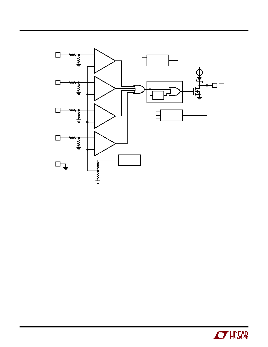
8
LTC2903-1
29031f
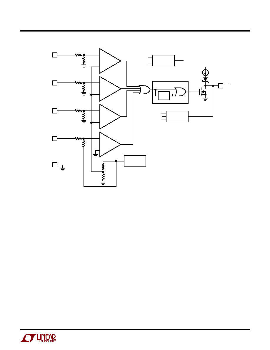
(LTC2903-B1)
BLOCK DIAGRA S
W
1
5V
V1
3
3.3V
V2
4
2.5V
V3
5
1.8V
V4
2
GND
≠
+
≠
+
≠
+
≠
+
RESET DELAY GENERATOR
200ms
DELAY
LOW VOLTAGE
PULL-DOWN
BANDGAP
REFERENCE
V1
V2
V3
V2
RST
10
µ
A
6
2903 BD2
POWER
DETECT
V1
V2
V
CC
9
LTC2903-1
29031f
(LTC2903-C1)
BLOCK DIAGRA S
W
1
5V
V1
3
3.3V
V2
4
1.8V
V3
5
≠5.2V
V4
2
GND
≠
+
≠
+
≠
+
≠
+
RESET DELAY GENERATOR
200ms
DELAY
LOW VOLTAGE
PULL-DOWN
BANDGAP
REFERENCE
V1
V2
V3
V2
RST
10
µ
A
6
2903 BD3
POWER
DETECT
V1
V2
V
CC

10
LTC2903-1
29031f
APPLICATIO S I FOR ATIO
W
U
U
U
Power-Up
The LTC2903-1 issues a logic low on the RST output when
an input supply voltage resides below the prescribed
threshold voltage. Ideally, the RST logic output would
remain low with the input supply voltage down to zero
volts. Most supervisors lack pull-down capability below
1V. The LTC2903-1 power supply supervisors incorporate
a new low voltage pull-down circuit that can hold the RST
line low with as little as 200mV of input supply voltage on
V1, V2 or V3. The pull-down circuit helps maintain a low
impedance path to ground, reducing the risk of floating the
RST node to undetermined voltages. Such voltages may
trigger external logic causing erroneous reset operation(s).
Furthermore, a mid-scale voltage could cause external
circuits to operate in the middle of their voltage transfer
characteristic, consuming more quiescent current than
normal. These conditions could cause serious system
reliability problems.
When V1, V2 and V3 are ramped simultaneously, the reset
pull-down current increases up to three times the current
that may be pulled with a single input. Figure 1 demon-
strates the reset pin current sinking ability for single
supply and triple supply-tracking applications. Figure 2
shows a detailed view of the reset pin voltage with a 10k
pull-up resistor to V1.
The LTC2903-1 supervisors derive their internal supply
voltage (V
CC
) automatically from the greater voltage on the
V1 and V2 inputs. With all supply inputs above threshold,
the quiescent current drawn from V
CC
is 20
µ
A (typ).
Supply Monitoring
The LTC2903-1 accurately monitors four inputs in a small
6-lead SOT-23 package. The low voltage reset output
includes an integrated 200ms reset delay timer. The reset
line pulls high 200ms after all voltage inputs exceed their
respective thresholds. The reset output remains low dur-
ing power-up, power-down and brownout conditions on
any of the voltage inputs.
For applications requiring an adjustable trip threshold, use
the V4 input on the LTC2903-A1. Connect the tap point on
an external resistive divider (R1, R2) placed between the
positive voltage being sensed and ground, to the high
impedance input on V4. The LTC2903-A1 compares the
voltage on the V4 pin to the internal 0.5V reference.
Figure 3 shows a generic setup for the positive adjustable
application.
Figure 3. Setting the Positive Adjustable Trip Point
V
CC
(V)
10
I
RST
(
µ
A)
1000
10000
0
0.8
1.2
29031 F01
1
0.4
0.2
1.0
0.6
100
V1 = V2 = V3
V1 ONLY
T
A
= 25
∞
C
V
RST
= 0.3V
CC
Figure 1. RST Pull-Down Current vs V
CC
V1 (V)
0
0
RST OUTPUT VOLTAGE (V)
0.1
0.3
0.4
0.5
0.7
0.1
0.5
0.7
39031 F02
0.2
0.6
0.4
0.9 1.0
0.2 0.3
0.6
0.8
T
A
= 25
∞
C
V1 ONLY
COMPETITION
PART
V1 = V2 = V3
≠
+
0.5V
29031 F03
V4
V
TRIP
R1
1%
LTC2903-A1
R2
1%
+
≠
Figure 2. RST Output Voltage with a 10k Pull-Up to V1
(Enlarged Area of Detail)

11
LTC2903-1
29031f
Calculate the trip voltage from:
V
V
R
R
TRIP
=
+
0 5
1
1
2
.
Table 1 contains suggested 1% resistor values for the ADJ
input to obtain nominal ≠11.5% thresholds.
Table 1. Suggested 1% Resistor Values for the ADJ Input
V
SUPPLY
(V)
V
TRIP
(V)
R1 (k
)
R2(k
)
12
10.75
2050
100
10
8.95
1690
100
8
7.15
1330
100
7.5
6.7
1240
100
6
5.38
976
100
5
4.435
787
100
3.3
2.935
487
100
3
2.66
432
100
2.5
2.2
340
100
1.8
1.605
221
100
1.5
1.325
165
100
1.2
1.065
113
100
1
0.884
76.8
100
0.9
0.795
59
100
Connect unused supervisor inputs to the highest supply
voltage available (typically V1). On the LTC2903-C1, the
negative V4 input must always be applied.
Implications of Threshold Accuracy
Specifying system voltage margin for worst-case opera-
tion requires consideration of three factors: power supply
tolerance, IC supply voltage tolerance and supervisor re-
set threshold accuracy. Highly accurate supervisors ease
the design challenge by decreasing the overall voltage
margin required for reliable system operation. Consider a
5V system with a
±
10% power supply tolerance band.
System ICs powered by this supply must operate reliably
within this band (and a little more, as explained below).
The bottom of the supply tolerance band, at 4.5V (5V ≠
10%), is the exact voltage at which a
perfectly accurate
supervisor generates a reset. Such a perfectly accurate
supervisor does not exist--the actual reset threshold may
vary over a specified band (
±
1.5% for the LTC2903-1 su-
pervisors). Figure 4 shows the typical relative threshold
accuracy for all four inputs, over temperature.
With this variation of reset threshold in mind, the nominal
reset threshold of the supervisor resides
below the mini-
mum supply voltage; just enough so that the reset thresh-
old band and the power supply tolerance bands do not
overlap. If the two bands overlap, the supervisor could
generate a false or nuisance reset when the power supply
remains within its specified tolerance band (say, at 4.6V).
Adding half of the reset threshold accuracy spread (1.5%)
to the ideal 10% thresholds puts the LTC2903-1 thresh-
olds at 11.5% (typ) below the nominal input voltage. For
example, the 5V typical threshold is 4.425V, or 75mV
below the ideal threshold of 4.500V. The guaranteed
threshold lies in the band between 4.500V and 4.350V
over temperature.
The powered system must work reliably down to the
lowest voltage in the threshold band or risk malfunction
before the reset line falls. In the 5V example, using the
1.5% accurate supervisor, the system ICs must work
down to 4.35V. System ICs working with a
±
2.5% accurate
supervisor must operate down to 4.25V, increasing the
required system voltage margin and the probability of
system malfunction.
APPLICATIO S I FOR ATIO
W
U
U
U
Figure 4. LTC2903 Typical Threshold Accuracy vs Temperature
TEMPERATURE (
∞
C)
≠50
≠1.5
TYPICAL THRESHOLD ACCURACY (%)
≠1.0
≠0.5
0
0.5
25
75
100
29031 F04
1.0
1.5
≠25
0
50
12
LTC2903-1
29031f
APPLICATIO S I FOR ATIO
W
U
U
U
In any supervisory application, supply noise riding on the
monitored DC voltage can cause spurious resets, particu-
larly when the monitored voltage approaches the reset
threshold. A less than desirable but commonly used
technique used to mitigate this problem adds hysteresis to
the input comparator. The amount of added hysteresis,
usually specified as a percentage of the trip threshold,
effectively degrades the advertised accuracy of the part.
To maintain high accuracy, the LTC2903-1 does not use
hysteresis.
To minimize spurious resets while maintaining threshold
accuracy, the LTC2903-1 employs two forms of noise
filtering. The first line of defense incorporates proprietary
tailoring of the comparator transient response. Transient
events receive electronic integration in the comparator
and must exceed a certain magnitude and duration to
cause the comparator to switch. Figure 5 illustrates the
typical transient duration versus comparator overdrive
(as a percentage of the trip threshold V
RT
) required to trip
the comparators. Once any comparator is switched, the
reset line pulls low. The reset time-out counter starts once
all inputs return above threshold. The nominal reset delay
time is 200ms. The counter clears whenever any input
drops back below threshold. This reset delay time effec-
tively provides further filtering of the voltage inputs. A
noisy input with frequency components of sufficient mag-
nitude above f = 1/t
RST
= 5Hz holds the reset line low,
preventing oscillatory behavior on the reset line.
Although all four comparators have built-in glitch filtering,
use bypass capacitors on the V1 and V2 inputs because
the greater of V1 or V2 supplies the V
CC
for the part (a
0.1
µ
F ceramic capacitor satisfies most applications). Ap-
ply filter capacitors on the V3 and V4 inputs in extremely
noisy situations.
Reset Output Rise and Fall Time Estimation
The reset output line contains a weak pull-up current
source to the V2 supply. Use an external pull-up resistor
when the output needs to pull to another voltage and/or
when the reset output needs a faster rise time. The open-
drain output allows for wired-OR connections when more
than one signal needs to pull down on the reset line.
Estimate output rise time for the open-drain output with-
out an external pull-up using:
t
RISE
2.2 ∑ R
PU
∑ C
LOAD
where R
PU
is the on-resistance of the pull-up transistor
and C
LOAD
is the external load capacitance on the pin. At
room temperature, the average R
PU
is approximately
50k
. When externally pulling up to voltages higher than
V2, an internal network automatically protects the weak
pull-up circuitry from reverse currents.
The reset output has very strong pull-down capability.
Estimate the output fall time using:
t
FALL
2.2 ∑ R
PD
∑ C
LOAD
where R
PD
is the on-resistance of the pull-down transistor
and C
LOAD
is the external load capacitance on the pin. At
room temperature, the average R
PD
is approximately 40
.
With a 150pF load capacitance the reset line can pull down
in about 13ns.
Figure 5. Typical Transient Duration vs Overdrive
Required to Trip Comparator
RESET COMPARATOR OVERDRIVE (% OF V
RTX
)
0.1
250
TYPICAL TRANSIENT DURATION (
µ
s)
300
350
400
1
10
100
29031 F05
200
150
50
0
100
RESET OCCURS
ABOVE CURVE
T
A
= 25
∞
C

13
LTC2903-1
29031f
TYPICAL APPLICATIO S
U
V1
GND
V2
SYSTEM RESET
1V
1.8V
RST
V4
V3
3.3V
2.5V
1
2
3
6
5
4
LTC2903-A1
R2
100k
2903 TA02
C1
0.1
µ
F
C2
0.1
µ
F
R1
76.8k
Quad Supply Monitor with Adjustable Input
Fixed Quad Supply Monitor with LED Indication on RST
V1
GND
V2
SYSTEM RESET
1.8V
2.5V
RST
V4
V3
5V
3.3V
1
2
3
6
5
4
LTC2903-B1
LED
1k
5V
2903 TA05
C1
0.1
µ
F
C2
0.1
µ
F

14
LTC2903-1
29031f
TYPICAL APPLICATIO S
U
Quad Supply Monitor with Unused Input Pulled Above Threshold
V1
GND
V2
SYSTEM RESET
≠5.2V
RST
V4
V3
5V
3.3V
1
2
3
6
5
4
LTC2903-C1
2903 TA03
C1
0.1
µ
F
C2
0.1
µ
F

15
LTC2903-1
29031f
U
PACKAGE DESCRIPTIO
S6 Package
6-Lead Plastic TSOT-23
(Reference LTC DWG # 05-08-1636)
1.50 ≠ 1.75
(NOTE 4)
2.80 BSC
0.30 ≠ 0.45
6 PLCS (NOTE 3)
DATUM `A'
0.09 ≠ 0.20
(NOTE 3)
S6 TSOT-23 0302
2.90 BSC
(NOTE 4)
0.95 BSC
1.90 BSC
0.80 ≠ 0.90
1.00 MAX
0.01 ≠ 0.10
0.20 BSC
0.30 ≠ 0.50 REF
PIN ONE ID
NOTE:
1. DIMENSIONS ARE IN MILLIMETERS
2. DRAWING NOT TO SCALE
3. DIMENSIONS ARE INCLUSIVE OF PLATING
4. DIMENSIONS ARE EXCLUSIVE OF MOLD FLASH AND METAL BURR
5. MOLD FLASH SHALL NOT EXCEED 0.254mm
6. JEDEC PACKAGE REFERENCE IS MO-193
3.85 MAX
0.62
MAX
0.95
REF
RECOMMENDED SOLDER PAD LAYOUT
PER IPC CALCULATOR
1.4 MIN
2.62 REF
1.22 REF
Information furnished by Linear Technology Corporation is believed to be accurate and reliable.
However, no responsibility is assumed for its use. Linear Technology Corporation makes no represen-
tation that the interconnection of its circuits as described herein will not infringe on existing patent rights.

16
LTC2903-1
29031f
©
LINEAR TECHNOLOGY CORPORATION 2003
LT/TP 1203 1K ∑ PRINTED IN THE USA
PART NUMBER
DESCRIPTION
COMMENTS
LTC690
5V Supply Monitor, Watchdog Timer and Battery Backup
4.65 Threshold
LTC694-3.3
3.3V Supply Monitor, Watchdog Timer and Battery Backup
2.9V Threshold
LTC699
5V Supply Monitor and Watchdog Timer
4.65 Threshold
LTC1232
5V Supply Monitor, Watchdog Timer and Pushbutton Reset
4.37V/4.62V Threshold
LTC1326
Micropower Precision Triple Supply Monitor for 5V, 3.3V and ADJ
4.725V, 3.118V, 1V Thresholds (
±
0.75%)
LTC1326-2.5
Micropower Precision Triple Supply Monitor for 2.5V, 3.3V and ADJ 2.363V, 3.118V, 1V Thresholds (
±
0.75%)
LTC1536
Precision triple Supply Monitor for PCI Applications
Meets PCI t
FAIL
Timing Specifications
LTC1726-2.5
Micropower Triple Supply Monitor for 2.5V, 3.3V and ADJ
Adjustable RESET and Watchdog Time Outs
LTC1726-5
Micropower Triple Supply Monitor for 5V, 3.3V and ADJ
Adjustable RESET and Watchdog Time Outs
LTC1727-2.5/LTC1727-5
Micropower Triple Supply Monitors with Open-Drain Reset
Individual Monitor Outputs in MSOP
LTC1728-1.8/LTC1728-3.3 Micropower Triple Supply Monitors with Open-Drain Reset
5-Lead SOT-23 Package
LTC1728-2.5/LTC1728-5
Micropower Triple Supply Monitors with Open-Drain Reset
5-Lead SOT-23 Package
LTC1985-1.8
Micropower Triple Supply Monitor with Push-Pull Reset Output
5-Lead SOT-23 Package
LTC2900
Quad Voltage Monitor in MSOP
16 User Selectable Combinations,
±
1.5% Threshold Accuracy
LTC2901
Quad Voltage Monitor with Watchdog
16 User Selectable Combinations, Adjustable Timers
LTC2902
Quad Voltage Monitor with RST Disable
16 User Selectable Combinations, Adjustable Tolerance
LTC2920-1/LTC2920-2
Single/Dual Power Supply Margining Controller
<0.4% Margin Voltage Precision
LTC2921/LTC2922
Power Supply Trackers with Input Monitors
3 (LTC2921) and 5 (LTC2922) Remote Sense Switches
LTC2923
Power Supply Tracking Controller
Tracks Up and Down, Supply Sequencing
RELATED PARTS
Linear Technology Corporation
1630 McCarthy Blvd., Milpitas, CA 95035-7417
(408) 432-1900
q
FAX: (408) 434-0507
q
www.linear.com
TYPICAL APPLICATIO
U
Quad Supply Monitor with Manual Reset Button
GND
V2
V4
V3
3.3V
2.5V
2
3
5
4
LTC2903-A1
RST
1
V1
6
SYSTEM RESET
1.8V
3.3V
R2
100k
*OPTIONAL RESISTOR RECOMMENDED
TO EXTEND ESD TOLERANCE
R1
2050k
R3
10k
2903 TA04
C1
0.1
µ
F
C2
0.1
µ
F
R
ESD
*
10k
MANUAL
RESET BUTTON
(NORMALLY OPEN)
12V
(V
TRIP
= 10.75V)