 | –≠–ª–µ–∫—Ç—Ä–æ–Ω–Ω—ã–π –∫–æ–º–ø–æ–Ω–µ–Ω—Ç: LTC6911-1 | –°–∫–∞—á–∞—Ç—å:  PDF PDF  ZIP ZIP |

LTC6911-1/LTC6911-2
1
sn691112 691112fs
, LTC and LT are registered trademarks of Linear Technology Corporation.
s
3-Bit Digital Gain Control:
(Inverting Gains of 0, 1, 2, 5, 10, 20, 50
and 100V/V) -1 Option
(Inverting Gains of 0, 1, 2, 4, 8, 16, 32
and 64V/V) -2 Option
s
Two Matched Programmable Gain Amplifiers
s
Channel-to-Channel Gain Matching of 0.1dB (Max)
s
Rail-to-Rail Input Range
s
Rail-to-Rail Output Swing
s
Single or Dual Supply: 2.7V to 10.5V Total
s
11MHz Gain Bandwidth Product
s
Input Noise: 10nV/
Hz
s
Total System Dynamic Range to 120dB
s
Input Offset Voltage: 2mV, Gain of 10
s
Low Profile 10-Lead MSOP Package
Dual Matched Amplifiers
with Digitally Programmable
Gain in MSOP
s
Data Acquisition Systems
s
Dynamic Gain Changing
s
Automatic Ranging Circuits
s
Automatic Gain Control
Frequency Response (LTC6911-1)
The LTC
Æ
6911 is a family of low noise digitally program-
mable gain amplifiers (PGAs) that are easy to use and
occupy very little PC board space. The matched gain of
both channels is adjustable using a 3-bit parallel interface
to select voltage gains of 0, 1, 2, 5, 10, 20, 50 and 100V/
V (LTC6911-1) and 0, 1, 2, 4, 8, 16, 32 and 64V/V
(LTC6911-2). All gains are inverting.
The LTC6911 family consists of two matched inverting
amplifiers with rail-to-rail outputs. When operated with
unity gain, they will also process rail-to-rail input signals.
A half-supply reference generated internally at the AGND
pin supports single power supply applications. Operating
from single or split supplies from 2.7V to 10.5V, the
LTC6911 family is offered in a 10-lead MSOP package.
FEATURES
DESCRIPTIO
U
APPLICATIO S
U
TYPICAL APPLICATIO
U
LTC6911-X
10
7
9
V
OUTB
=
GAIN ∑ V
INB
V
OUTA
=
GAIN ∑ V
INA
8
1
V
INA
AGND
V
INB
3
2
1
µ
F
0.1
µ
F
V
+
2.7V TO 10.5V
4
5
6
691112 TA01
G0
G1
G2
G2
0
0
0
0
1
1
1
1
G1
0
0
1
1
0
0
1
1
G0
0
1
0
1
0
1
0
1
LTC6911-1
0
≠1
≠2
≠5
≠10
≠20
≠50
≠100
LTC6911-2
0
≠1
≠2
≠4
≠8
≠16
≠32
≠64
DIGITAL
INPUT
GAIN IN V/V
FREQUENCY (Hz)
10
GAIN (dB)
30
50
0
20
40
100
10k
100k
1M
10M
691112 TA02
≠10
1k
GAIN OF ≠100 (DIGITAL INPUT 111)
GAIN OF ≠1 (DIGITAL INPUT 001)
GAIN OF ≠2 (DIGITAL INPUT 010)
GAIN OF ≠5 (DIGITAL INPUT 011)
GAIN OF ≠10 (DIGITAL INPUT 100)
GAIN OF ≠20 (DIGITAL INPUT 101)
GAIN OF ≠50 (DIGITAL INPUT 110)
V
S
= 10V, V
IN
= 5mV
RMS

LTC6911-1/LTC6911-2
2
sn691112 691112fs
Total Supply Voltage (V
+
to V
≠
) .............................. 11V
Input Current .....................................................
±
10mA
Operating Temperature Range (Note 2)
LTC6911C-1/LTC6911C-2 .................. ≠ 40
∞
C to 85
∞
C
LTC6911I-1/LTC6911I-2 .................... ≠ 40
∞
C to 85
∞
C
LTC6911H-1/LTC6911H-2 ................ ≠ 40
∞
C to 125
∞
C
Specified Temperature Range (Note 3)
LTC6911C-1/LTC6911C-2 .................. ≠ 40
∞
C to 85
∞
C
LTC6911I-1/LTC6911I-2 .................... ≠ 40
∞
C to 85
∞
C
LTC6911H-1/LTC6911H-2 ................ ≠ 40
∞
C to 125
∞
C
Storage Temperature Range ................. ≠ 65
∞
C to 150
∞
C
Lead Temperature (Soldering, 10 sec).................. 300
∞
C
ORDER PART NUMBER
T
JMAX
= 150
∞
C,
JA
= 230
∞
C/W
LTC6911CMS-1
LTC6911IMS-1
LTC6911HMS-1
LTC6911CMS-2
LTC6911IMS-2
LTC6911HMS-2
(Note 1)
ABSOLUTE AXI U RATI GS
W
W
W
U
PACKAGE/ORDER I FOR ATIO
U
U
W
Table 1 (LTC6911-1)
NOMINAL
NOMINAL
INPUT
DIGITAL INPUTS
VOLTAGE GAIN
Dual 5V
Single 5V
Single 3V
IMPEDANCE
G2
G1
G0
Volts/Volt
(dB)
Supply
Supply
Supply
(k
)
0
0
0
0
≠120
10
5
3
(Open)
0
0
1
≠1
0
10
5
3
10
0
1
0
≠2
6
5
2.5
1.5
5
0
1
1
≠5
14
2
1
0.6
2
1
0
0
≠10
20
1
0.5
0.3
1
1
0
1
≠20
26
0.5
0.25
0.15
1
1
1
0
≠50
34
0.2
0.1
0.06
1
1
1
1
≠100
40
0.1
0.05
0.03
1
GAI SETTI GS A D PROPERTIES
U
U
U
1
2
3
4
5
INA
AGND
INB
G0
G1
10
9
8
7
6
OUTA
V
≠
OUTB
V
+
G2
TOP VIEW
MS PACKAGE
10-LEAD PLASTIC MSOP
Consult LTC Marketing for parts specified with wider operating temperature ranges.
MAXIMUM LINEAR INPUT RANGE (V
P-P
)
MS PART MARKING
LTAHK
LTAHM
LTBCF
LTAHH
LTAHJ
LTBCG
Table 2 (LTC6911-2)
NOMINAL
NOMINAL
INPUT
DIGITAL INPUTS
VOLTAGE GAIN
Dual 5V
Single 5V
Single 3V
IMPEDANCE
G2
G1
G0
Volts/Volt
(dB)
Supply
Supply
Supply
(k
)
0
0
0
0
≠120
10
5
3
(Open)
0
0
1
≠1
0
10
5
3
10
0
1
0
≠2
6
5
2.5
1.5
5
0
1
1
≠4
12
2.5
1.25
0.75
2.5
1
0
0
≠8
18.1
1.25
0.625
0.375
1.25
1
0
1
≠16
24.1
0.625
0.3125
0.188
1.25
1
1
0
≠32
30.1
0.3125
0.156
0.094
1.25
1
1
1
≠64
36.1
0.156
0.078
0.047
1.25
MAXIMUM LINEAR INPUT RANGE (V
P-P
)

LTC6911-1/LTC6911-2
3
sn691112 691112fs
The
q
denotes the specifications that apply over the full operating
temperature range, otherwise specifications are at T
A
= 25
∞
C. V
S
= 5V, AGND = 2.5V, Gain = 1 (Digital Inputs 001), R
L
= 10k
to midsupply point, unless otherwise noted.
ELECTRICAL CHARACTERISTICS
C/I GRADES
H GRADE
PARAMETER
CONDITIONS
MIN
TYP
MAX
MIN
TYP
MAX
UNITS
LTC6911-1/LTC6911-2
Total Supply Voltage (V
S
)
q
2.7
10.5
2.7
10.5
V
Supply Current per Channel
V
S
= 2.7V, V
INA
= V
INB
= V
AGND
q
2.1
3.15
2.1
3.25
mA
V
S
= 5V, V
INA
= V
INB
= V
AGND
q
2.5
3.75
2.5
4.00
mA
V
S
=
±
5V, V
INA
= V
INB
= 0V, Pins 4, 5, 6 = ≠4.5V or 5V
q
3.1
4.65
3.1
5.00
mA
V
S
=
±
5V, V
INA
= V
INB
= 0V, Pin 4 = 4.5V,
q
3.1
4.65
3.1
5.00
mA
Pins 5, 6 = 0.5V
Output Voltage Swing LOW (Note 4)
V
S
= 2.7V, R
L
= 10k Tied to Mid Supply
q
12
30
12
35
mV
V
S
= 2.7V, R
L
= 500
Tied to Mid Supply
q
60
110
60
125
mV
V
S
= 5V, R
L
= 10k Tied to Mid Supply
q
20
40
20
45
mV
V
S
= 5V, R
L
= 500
Tied to Mid Supply
q
100
170
100
190
mV
V
S
=
±
5V, R
L
= 10k Tied to 0V
q
30
50
30
60
mV
V
S
=
±
5V, R
L
= 500
Tied to 0V
q
190
260
190
290
mV
Output Voltage Swing HIGH (Note 4)
V
S
= 2.7V, R
L
= 10k Tied to Mid Supply
q
10
20
10
25
mV
V
S
= 2.7V, R
L
= 500
Tied to Mid Supply
q
50
80
50
90
mV
V
S
= 5V, R
L
= 10k Tied to Mid Supply
q
10
30
10
35
mV
V
S
= 5V, R
L
= 500
Tied to Mid Supply
q
90
160
90
175
mV
V
S
=
±
5V, R
L
= 10k Tied to 0V
q
20
40
20
45
mV
V
S
=
±
5V, R
L
= 500
Tied to 0V
q
180
250
180
270
mV
Output Short-Circuit Current (Note 5)
V
S
= 2.7V
q
±
27
±
27
mA
V
S
=
±
5V
q
±
35
±
35
mA
AGND Open-Circuit Voltage
V
S
= 5V
q
2.45
2.5
2.55
2.45
2.5
2.55
V
AGND (Common Mode)
V
S
= 2.7V
q
0.55
1.60
0.55
1.60
V
Input Voltage Range
V
S
= 5V
q
0.75
3.65
0.75
3.65
V
V
S
=
±
5V
q
≠ 4.30
3.20
≠ 4.30
3.20
V
AGND Rejection (i.e., Common
V
S
= 2.7V, V
AGND
= 1.1V to 1.6V
q
55
80
50
80
dB
Mode Rejection or CMRR)
V
S
=
±
5V, V
AGND
= ≠ 2.5V to 2.5V
q
55
75
50
75
dB
Power Supply Rejection Ratio (PSRR)
V
S
= 2.7V to
±
5V
q
60
80
57
80
dB
Slew Rate
V
S
= 5V, V
OUTA
= V
OUTB
= 1.1V to 3.9V
12
12
V/
µ
s
V
S
=
±
5V, V
OUTA
= V
OUTB
=
±
1.4V
16
16
V/
µ
s
Signal Attenuation at Gain = 0 Setting
Gain = 0 (Digital Inputs 000), f = 20kHz
q
≠ 120
≠ 120
dB
Digital Input "High" Voltage
V
S
= 2.7V
q
2.43
2.43
V
V
S
= 5V
q
4.50
4.50
V
V
S
=
±
5V
q
4.50
4.50
V
Digital Input "Low" Voltage
V
S
= 2.7V
q
0.27
0.27
V
V
S
= 5V
q
0.50
0.50
V
V
S
=
±
5V
q
0.50
0.50
V
Digital Input "High" Current
V
S
= 2.7V, Pins 4, 5, 6 = 2.43V
q
1
1
µ
A
V
S
= 5V, Pins 4, 5, 6 = 4.5V
q
5
5
µ
A
V
S
=
±
5V, Pins 4, 5, 6 = 4.5V
q
10
10
µ
A
Digital Input "Low" Current
V
S
= 2.7V, Pins 4, 5, 6 = 0.27V
q
1
1
µ
A
V
S
= 5V, Pins 4, 5, 6 = 0.5V
q
5
5
µ
A
V
S
=
±
5V, Pins 4, 5, 6 = 0.5V
q
10
10
µ
A
LTC6911-1/LTC6911-2
4
sn691112 691112fs
The
q
denotes the specifications that apply over the full operating
temperature range, otherwise specifications are at T
A
= 25
∞
C. V
S
= 5V, AGND = 2.5V, Gain = 1 (Digital Inputs 001), R
L
= 10k
to midsupply point, unless otherwise noted.
ELECTRICAL CHARACTERISTICS
LTC6911-1 Only
Voltage Gain (Note 6)
V
S
= 2.7V, Gain = 1, R
L
= 10k
q
≠0.07
0
0.07
≠0.08
0
0.07
dB
V
S
= 2.7V, Gain = 1, R
L
= 500
q
≠0.11 ≠0.02 0.07
≠0.13 ≠0.02 0.07
dB
V
S
= 2.7V, Gain = 2, R
L
= 10k
q
5.94 6.01
6.08
5.93
6.01
6.08
dB
V
S
= 2.7V, Gain = 5, R
L
= 10k
q
13.85 13.95 14.05
13.8 13.95 14.05
dB
V
S
= 2.7V, Gain = 10, R
L
= 10k
q
19.7 19.93 20.1
19.65 19.93 20.1
dB
V
S
= 2.7V, Gain = 10, R
L
= 500
q
19.6 19.85 20.1
19.45 19.85 20.1
dB
V
S
= 2.7V, Gain = 20, R
L
= 10k
q
25.75 25.94 26.1
25.65 25.94 26.1
dB
V
S
= 2.7V, Gain = 50, R
L
= 10k
q
33.5 33.8
34.1
33.4
33.8
34.1
dB
V
S
= 2.7V, Gain = 100, R
L
= 10k
q
39.0 39.6
40.1
38.8
39.6
40.1
dB
V
S
= 2.7V, Gain = 100, R
L
= 500
q
37.4 38.9
40.1
36.5
38.9
40.1
dB
V
S
= 5V, Gain = 1, R
L
= 10k
q
≠0.08 0.01
0.08
≠0.09 0.01
0.08
dB
V
S
= 5V, Gain = 1, R
L
= 500
q
≠0.11 ≠0.01 0.07
≠0.13 ≠0.01 0.07
dB
V
S
= 5V, Gain = 2, R
L
= 10k
q
5.95 6.02
6.09
5.94
6.02
6.09
dB
V
S
= 5V, Gain = 5, R
L
= 10k
q
13.8 13.96 14.1
13.78 13.96 14.1
dB
V
S
= 5V, Gain = 10, R
L
= 10k
q
19.8 19.94 20.1
19.75 19.94 20.1
dB
V
S
= 5V, Gain = 10, R
L
= 500
q
19.6 19.87 20.1
19.45 19.87 20.1
dB
V
S
= 5V, Gain = 20, R
L
= 10k
q
25.8 25.94 26.1
25.75 25.94 26.1
dB
V
S
= 5V, Gain = 50, R
L
= 10k
q
33.5 33.84 34.1
33.4 33.84 34.1
dB
V
S
= 5V, Gain = 100, R
L
= 10k
q
39.3 39.7
40.1
39.1
39.7
40.1
dB
V
S
= 5V, Gain = 100, R
L
= 500
q
38.0 39.2
40.1
37.0
39.2
40.1
dB
V
S
=
±
5V, Gain = 1, R
L
= 10k
q
≠0.06 0.01
0.08
≠0.07 0.01
0.08
dB
V
S
=
±
5V, Gain = 1, R
L
= 500
q
≠0.10 0.00
0.08
≠0.11 0.00
0.08
dB
V
S
=
±
5V, Gain = 2, R
L
= 10k
q
5.95 6.02
6.09
5.94
6.02
6.09
dB
V
S
=
±
5V, Gain = 5, R
L
= 10k
q
13.8 13.96 14.1
13.79 13.96 14.1
dB
V
S
=
±
5V, Gain = 10, R
L
= 10k
q
19.8 19.94 20.1
19.75 19.94 20.1
dB
V
S
=
±
5V, Gain = 10, R
L
= 500
q
19.7 19.91 20.1
19.60 19.91 20.1
dB
V
S
=
±
5V, Gain = 20, R
L
= 10k
q
25.8 25.95 26.1
25.75 25.95 26.1
dB
V
S
=
±
5V, Gain = 50, R
L
= 10k
q
33.7 33.87 34.1
33.60 33.87 34.1
dB
V
S
=
±
5V, Gain = 100, R
L
= 10k
q
39.4 39.8
40.2
39.25 39.8
40.2
dB
V
S
=
±
5V, Gain = 100, R
L
= 500
q
38.8 39.5
40.1
38.00 39.5
40.1
dB
Channel-to-Channel Voltage
V
S
= 2.7V, Gain = 1, R
L
= 10k
q
≠0.1 0.02
0.1
≠0.1
0.02
0.1
dB
Gain Match
V
S
= 2.7V, Gain = 1, R
L
= 500
q
≠0.1 0.02
0.1
≠0.1
0.02
0.1
dB
V
S
= 2.7V, Gain = 2, R
L
= 10k
q
≠0.1 0.02
0.1
≠0.1
0.02
0.1
dB
V
S
= 2.7V, Gain = 5, R
L
= 10k
q
≠0.15 0.02
0.15
≠0.15 0.02
0.15
dB
V
S
= 2.7V, Gain = 10, R
L
= 10k
q
≠0.15 0.02
0.15
≠0.15 0.02
0.15
dB
V
S
= 2.7V, Gain = 10, R
L
= 500
q
≠0.15 0.02
0.15
≠0.15 0.02
0.15
dB
V
S
= 2.7V, Gain = 20, R
L
= 10k
q
≠0.15 0.02
0.15
≠0.15 0.02
0.15
dB
V
S
= 2.7V, Gain = 50, R
L
= 10k
q
≠0.15 0.02
0.15
≠0.15 0.02
0.15
dB
V
S
= 2.7V, Gain = 100, R
L
= 10k
q
≠0.20 0.02
0.20
≠0.20 0.02
0.20
dB
V
S
= 2.7V, Gain = 100, R
L
= 500
q
≠1.00 0.02
1.00
≠1.50 0.02
1.50
dB
C/I GRADES
H GRADE
PARAMETER
CONDITIONS
MIN
TYP
MAX
MIN
TYP
MAX
UNITS
LTC6911-1/LTC6911-2
5
sn691112 691112fs
The
q
denotes the specifications that apply over the full operating
temperature range, otherwise specifications are at T
A
= 25
∞
C. V
S
= 5V, AGND = 2.5V, Gain = 1 (Digital Inputs 001), R
L
= 10k
to midsupply point, unless otherwise noted.
ELECTRICAL CHARACTERISTICS
C/I GRADES
H GRADE
PARAMETER
CONDITIONS
MIN
TYP
MAX
MIN
TYP
MAX
UNITS
LTC6911-1 Only
Channel-to-Channel Voltage
V
S
= 5V, Gain = 1, R
L
= 10k
q
≠0.1 0.02
0.1
≠0.1
0.02
0.1
dB
Gain Match
V
S
= 5V, Gain = 1, R
L
= 500
q
≠0.1 0.02
0.1
≠0.1
0.02
0.1
dB
V
S
= 5V, Gain = 2, R
L
= 10k
q
≠0.1 0.02
0.1
≠0.1
0.02
0.1
dB
V
S
= 5V, Gain = 5, R
L
= 10k
q
≠0.15 0.02
0.15
≠0.15 0.02
0.15
dB
V
S
= 5V, Gain = 10, R
L
= 10k
q
≠0.15 0.02
0.15
≠0.15 0.02
0.15
dB
V
S
= 5V, Gain = 10, R
L
= 500
q
≠0.15 0.02
0.15
≠0.15 0.02
0.15
dB
V
S
= 5V, Gain = 20, R
L
= 10k
q
≠0.15 0.02
0.15
≠0.15 0.02
0.15
dB
V
S
= 5V, Gain = 50, R
L
= 10k
q
≠0.15 0.02
0.15
≠0.15 0.02
0.15
dB
V
S
= 5V, Gain = 100, R
L
= 10k
q
≠0.2 0.02
0.2
≠0.2
0.02
0.2
dB
V
S
= 5V, Gain = 100, R
L
= 500
q
≠0.8 0.02
0.8
≠1.2
0.02
1.2
dB
V
S
=
±
5V, Gain = 1, R
L
= 10k
q
≠0.1 0.02
0.1
≠0.1
0.02
0.1
dB
V
S
=
±
5V, Gain = 1, R
L
= 500
q
≠0.1 0.02
0.1
≠0.1
0.02
0.1
dB
V
S
=
±
5V, Gain = 2, R
L
= 10k
q
≠0.1 0.02
0.1
≠0.1
0.02
0.1
dB
V
S
=
±
5V, Gain = 5, R
L
= 10k
q
≠0.15 0.02
0.15
≠0.15 0.02
0.15
dB
V
S
=
±
5V, Gain = 10, R
L
= 10k
q
≠0.15 0.02
0.15
≠0.15 0.02
0.15
dB
V
S
=
±
5V, Gain = 10, R
L
= 500
q
≠0.15 0.02
0.15
≠0.15 0.02
0.15
dB
V
S
=
±
5V, Gain = 20, R
L
= 10k
q
≠0.15 0.02
0.15
≠0.15 0.02
0.15
dB
V
S
=
±
5V, Gain = 50, R
L
= 10k
q
≠0.15 0.02
0.15
≠0.15 0.02
0.15
dB
V
S
=
±
5V, Gain = 100, R
L
= 10k
q
≠0.2 0.02
0.2
≠0.2
0.02
0.2
dB
V
S
=
±
5V, Gain = 100, R
L
= 500
q
≠0.6 0.02
0.6
≠0.9
0.02
0.9
dB
Gain Temperature Coefficient
V
S
= 5V, Gain = 1, R
L
= Open
2
2
ppm/
∞
C
V
S
= 5V, Gain = 2, R
L
= Open
≠1.5
≠1.5
ppm/
∞
C-
V
S
= 5V, Gain = 5, R
L
= Open
≠11
≠11
ppm/
∞
C
V
S
= 5V, Gain = 10, R
L
= Open
≠30
≠30
ppm/
∞
C
V
S
= 5V, Gain = 20, R
L
= Open
≠38
≠38
ppm/
∞
C
V
S
= 5V, Gain = 50, R
L
= Open
≠70
≠70
ppm/
∞
C
V
S
= 5V, Gain = 100, R
L
= Open
≠140
≠140
ppm/
∞
C
Channel-to-Channel Gain Temperature V
S
= 5V, Gain = 1, R
L
= Open
1.0
1.0
ppm/
∞
C
Coefficient Match
V
S
= 5V, Gain = 2, R
L
= Open
1.0
1.0
ppm/
∞
C
V
S
= 5V, Gain = 5, R
L
= Open
0.2
0.2
ppm/
∞
C
V
S
= 5V, Gain = 10, R
L
= Open
1.0
1.0
ppm/
∞
C
V
S
= 5V, Gain = 20, R
L
= Open
0.4
0.4
ppm/
∞
C
V
S
= 5V, Gain = 50, R
L
= Open
3.0
3.0
ppm/
∞
C
V
S
= 5V, Gain = 100, R
L
= Open
3.0
3.0
ppm/
∞
C
Channel-to-Channel Isolation (Note 7)
f = 200kHz
V
S
= 5V, Gain = 1, R
L
= 10k
108
108
dB
V
S
= 5V, Gain = 10, R
L
= 10k
107
107
dB
V
S
= 5V, Gain = 100, R
L
= 10k
93
93
dB
Offset Voltage Magnitude Referred
Gain = 1
q
2.0
22
2.0
22
mV
to INA or INB Pins (Note 8)
Gain = 10
q
1.1
12
1.1
14
mV
Offset Voltage Magnitude Drift
Gain = 1
12
20
µ
V/
∞
C
Referred to INA or INB Pins (Note 8)
Gain = 10
6.6
11
µ
V/
∞
C
LTC6911-1/LTC6911-2
6
sn691112 691112fs
The
q
denotes the specifications that apply over the full operating
temperature range, otherwise specifications are at T
A
= 25
∞
C. V
S
= 5V, AGND = 2.5V, Gain = 1 (Digital Inputs 001), R
L
= 10k
to midsupply point, unless otherwise noted.
ELECTRICAL CHARACTERISTICS
C/I GRADES
H GRADE
PARAMETER
CONDITIONS
MIN
TYP
MAX
MIN
TYP
MAX
UNITS
LTC6911-1 Only
DC Input Resistance at
DC V
INA
or V
INB
= 0V
INA or INB Pins (Note 9)
Gain = 0
q
>100
>100
M
Gain = 1
q
10
10
k
Gain = 2
q
5
5
k
Gain = 5
q
2
2
k
Gain > 5
q
1
1
k
DC Input Resistance Match
Gain = 1
q
10
10
R
INA
≠ R
INB
Gain = 2
q
5
5
Gain = 5
q
2
2
Gain > 5
q
1
1
DC Small-Signal Output Resistance
DC V
INA
or V
INB
= 0V
at OUTA or OUTB Pins
Gain = 0
0.4
0.4
Gain = 1
0.7
0.7
Gain = 2
1.0
1.0
Gain = 5
1.9
1.9
Gain = 10
3.4
3.4
Gain = 20
6.4
6.4
Gain = 50
15
15
Gain = 100
30
30
Gain-Bandwidth Product
Gain = 100, f
IN
= 200kHz
q
7
11
18
6
11
18
MHz
Wideband Noise (Referred to Input)
f = 1kHz to 200kHz
Gain = 0 (Output Noise Only)
7.5
7.5
µ
V
RMS
Gain = 1
12.3
12.3
µ
V
RMS
Gain = 2
8.5
8.5
µ
V
RMS
Gain = 5
6.1
6.1
µ
V
RMS
Gain = 10
5.2
5.2
µ
V
RMS
Gain = 20
5.0
5.0
µ
V
RMS
Gain = 50
4.5
4.5
µ
V
RMS
Gain = 100
3.8
3.8
µ
V
RMS
Voltage Noise Density
f = 50kHz
(Referred to Input)
Gain = 1
28
28
nV/
Hz
Gain = 2
19
19
nV/
Hz
Gain = 5
14
14
nV/
Hz
Gain = 10
12
12
nV/
Hz
Gain = 20
11.5
11.5
nV/
Hz
Gain = 50
10.8
10.8
nV/
Hz
Gain = 100
9.9
9.9
nV/
Hz
Total Harmonic Distortion
Gain = 10, f
IN
= 10kHz, V
OUT
= 1V
RMS
≠ 90
≠ 90
dB
0.003
0.003
%
Gain = 10, f
IN
= 100kHz, V
OUT
= 1V
RMS
≠ 82
≠ 82
dB
0.008
0.008
%
LTC6911-1/LTC6911-2
7
sn691112 691112fs
The
q
denotes the specifications that apply over the full operating
temperature range, otherwise specifications are at T
A
= 25
∞
C. V
S
= 5V, AGND = 2.5V, Gain = 1 (Digital Inputs 001), R
L
= 10k
to midsupply point, unless otherwise noted.
ELECTRICAL CHARACTERISTICS
LTC6911-2 Only
Voltage Gain (Note 6)
V
S
= 2.7V, Gain = 1, R
L
= 10k
q
≠0.07
0
0.07
≠0.08
0
0.07
dB
V
S
= 2.7V, Gain = 1, R
L
= 500
q
≠0.11 ≠0.02 0.07
≠0.13 ≠0.02 0.07
dB
V
S
= 2.7V, Gain = 2, R
L
= 10k
q
5.94 6.01
6.08
5.93
6.01
6.08
dB
V
S
= 2.7V, Gain = 4, R
L
= 10k
q
11.9 12.02 12.12
11.88 12.02 12.12
dB
V
S
= 2.7V, Gain = 8, R
L
= 10k
q
17.80 18.00 18.15
17.75 18.00 18.15
dB
V
S
= 2.7V, Gain = 8, R
L
= 500
q
17.65 17.94 18.15
17.55 17.94 18.15
dB
V
S
= 2.7V, Gain = 16, R
L
= 10k
q
23.8 24.01 24.25
23.75 24.01 24.25
dB
V
S
= 2.7V, Gain = 32, R
L
= 10k
q
29.7
30
30.2
29.65
30
30.2
dB
V
S
= 2.7V, Gain = 64, R
L
= 10k
q
35.3 35.8
36.2
35.15 35.8
36.2
dB
V
S
= 2.7V, Gain = 64, R
L
= 500
q
34.2 35.3
36.2
33.65 35.3
36.2
dB
V
S
= 5V, Gain = 1, R
L
= 10k
q
≠0.08 0.00
0.08
≠0.09 0.00
0.08
dB
V
S
= 5V, Gain = 1, R
L
= 500
q
≠0.10 ≠0.01 0.08
≠0.12 ≠0.01 0.08
dB
V
S
= 5V, Gain = 2, R
L
= 10k
q
5.96 6.02
6.1
5.95
6.02
6.1
dB
V
S
= 5V, Gain = 4, R
L
= 10k
q
11.85 12.02 12.15
11.83 12.02 12.15
dB
V
S
= 5V, Gain = 8, R
L
= 10k
q
17.85 18.01 18.15
17.83 18.01 18.15
dB
V
S
= 5V, Gain = 8, R
L
= 500
q
17.65 17.96 18.15
17.50 17.96 18.15
dB
V
S
= 5V, Gain = 16, R
L
= 10k
q
23.85 24.02 24.15
23.80 24.02 24.15
dB
V
S
= 5V, Gain = 32, R
L
= 10k
q
29.70 30.02 30.2
29.65 30.02 30.2
dB
V
S
= 5V, Gain = 64, R
L
= 10k
q
35.5 35.9
36.3
35.40 35.9
36.3
dB
V
S
= 5V, Gain = 64, R
L
= 500
q
34.7 35.6
36.1
34.20 35.6
36.1
dB
V
S
=
±
5V, Gain = 1, R
L
= 10k
q
≠0.06 0.01
0.08
≠0.07 0.01
0.08
dB
V
S
=
±
5V, Gain = 1, R
L
= 500
q
≠0.10 0.00
0.08
≠0.11 0.00
0.08
dB
V
S
=
±
5V, Gain = 2, R
L
= 10k
q
5.96 6.02
6.1
5.95
6.02
6.1
dB
V
S
=
±
5V, Gain = 4, R
L
= 10k
q
11.9 12.03 12.15
11.88 12.03 12.15
dB
V
S
=
±
5V, Gain = 8, R
L
= 10k
q
17.85 18.02 18.15
17.83 18.02 18.15
dB
V
S
=
±
5V, Gain = 8, R
L
= 500
q
17.80 17.99 18.15
17.73 17.99 18.15
dB
V
S
=
±
5V, Gain = 16, R
L
= 10k
q
23.85 24.03 24.15
23.82 24.03 24.15
dB
V
S
=
±
5V, Gain = 32, R
L
= 10k
q
29.85
30
30.2
29.8
30
30.2
dB
V
S
=
±
5V, Gain = 64, R
L
= 10k
q
35.65 36.0 36.20
35.55 36.0 36.20
dB
V
S
=
±
5V, Gain = 64, R
L
= 500
q
35.20 35.8 36.20
34.80 35.8 36.20
dB
Channel-to-Channel
V
S
= 2.7V, Gain = 1, R
L
= 10k
q
≠0.1 0.02
0.1
≠0.1
0.02
0.1
dB
Voltage Gain Match
V
S
= 2.7V, Gain = 1, R
L
= 500
q
≠0.1 0.02
0.1
≠0.1
0.02
0.1
dB
V
S
= 2.7V, Gain = 2, R
L
= 10k
q
≠0.1 0.02
0.1
≠0.1
0.02
0.1
dB
V
S
= 2.7V, Gain = 4, R
L
= 10k
q
≠0.15 0.02
0.15
≠0.15 0.02
0.15
dB
V
S
= 2.7V, Gain = 8, R
L
= 10k
q
≠0.15 0.02
0.15
≠0.15 0.02
0.15
dB
V
S
= 2.7V, Gain = 8, R
L
= 500
q
≠0.15 0.02
0.15
≠0.15 0.02
0.15
dB
V
S
= 2.7V, Gain = 16, R
L
= 10k
q
≠0.15 0.02
0.15
≠0.15 0.02
0.15
dB
V
S
= 2.7V, Gain = 32, R
L
= 10k
q
≠0.15 0.02
0.15
≠0.15 0.02
0.15
dB
V
S
= 2.7V, Gain = 64, R
L
= 10k
q
≠0.2 0.02
0.2
≠0.2
0.02
0.2
dB
V
S
= 2.7V, Gain = 64, R
L
= 500
q
≠0.7 0.02
0.7
≠1.0
0.02
1.0
dB
C/I GRADES
H GRADE
PARAMETER
CONDITIONS
MIN
TYP
MAX
MIN
TYP
MAX
UNITS

LTC6911-1/LTC6911-2
8
sn691112 691112fs
The
q
denotes the specifications that apply over the full operating
temperature range, otherwise specifications are at T
A
= 25
∞
C. V
S
= 5V, AGND = 2.5V, Gain = 1 (Digital Inputs 001), R
L
= 10k
to midsupply point, unless otherwise noted.
ELECTRICAL CHARACTERISTICS
C/I GRADES
H GRADE
PARAMETER
CONDITIONS
MIN
TYP
MAX
MIN
TYP
MAX
UNITS
LTC6911-2 Only
V
S
= 5V, Gain = 1, R
L
= 10k
q
≠0.1 0.02
0.1
≠0.1
0.02
0.1
dB
V
S
= 5V, Gain = 1, R
L
= 500
q
≠0.1 0.02
0.1
≠0.1
0.02
0.1
dB
V
S
= 5V, Gain = 2, R
L
= 10k
q
≠0.1 0.02
0.1
≠0.1
0.02
0.1
dB
V
S
= 5V, Gain = 4, R
L
= 10k
q
≠0.15 0.02
0.15
≠0.15 0.02
0.15
dB
V
S
= 5V, Gain = 8, R
L
= 10k
q
≠0.15 0.02
0.15
≠0.15 0.02
0.15
dB
V
S
= 5V, Gain = 8, R
L
= 500
q
≠0.15 0.02
0.15
≠0.15 0.02
0.15
dB
V
S
= 5V, Gain = 16, R
L
= 10k
q
≠0.15 0.02
0.15
≠0.15 0.02
0.15
dB
V
S
= 5V, Gain = 32, R
L
= 10k
q
≠0.15 0.02
0.15
≠0.15 0.02
0.15
dB
V
S
= 5V, Gain = 64, R
L
= 10k
q
≠0.15 0.02
0.15
≠0.15 0.02
0.15
dB
V
S
= 5V, Gain = 64, R
L
= 500
q
≠0.60 0.02
0.60
≠0.80 0.02
0.80
dB
V
S
=
±
5V, Gain = 1, R
L
= 10k
q
≠0.1 0.02
0.1
≠0.1
0.02
0.1
dB
V
S
=
±
5V, Gain = 1, R
L
= 500
q
≠0.1 0.02
0.1
≠0.1
0.02
0.1
dB
V
S
=
±
5V, Gain = 2, R
L
= 10k
q
≠0.1 0.02
0.1
≠0.1
0.02
0.1
dB
V
S
=
±
5V, Gain = 4, R
L
= 10k
q
≠0.15 0.02
0.15
≠0.15 0.02
0.15
dB
V
S
=
±
5V, Gain = 8, R
L
= 10k
q
≠0.15 0.02
0.15
≠0.15 0.02
0.15
dB
V
S
=
±
5V, Gain = 8, R
L
= 500
q
≠0.15 0.02
0.15
≠0.15 0.02
0.15
dB
V
S
=
±
5V, Gain = 16, R
L
= 10k
q
≠0.15 0.02
0.15
≠0.15 0.02
0.15
dB
V
S
=
±
5V, Gain = 32, R
L
= 10k
q
≠0.15 0.02
0.15
≠0.15 0.02
0.15
dB
V
S
=
±
5V, Gain = 64, R
L
= 10k
q
≠0.15 0.02
0.15
≠0.15 0.02
0.15
dB
V
S
=
±
5V, Gain = 64, R
L
= 500
q
≠0.40 0.02
0.40
≠0.60 0.02
0.60
dB
Gain Temperature Coefficient
V
S
= 5V, Gain = 1, R
L
= Open
2
2
ppm/
∞
C
V
S
= 5V, Gain = 2, R
L
= Open
≠1
≠1
ppm/
∞
C
V
S
= 5V, Gain = 4, R
L
= Open
≠7
≠7
ppm/
∞
C
V
S
= 5V, Gain = 8, R
L
= Open
≠21
≠21
ppm/
∞
C
V
S
= 5V, Gain = 16, R
L
= Open
≠28
≠28
ppm/
∞
C
V
S
= 5V, Gain = 32, R
L
= Open
≠40
≠40
ppm/
∞
C
V
S
= 5V, Gain = 64, R
L
= Open
≠115
≠115
ppm/
∞
C
Channel-to-Channel Gain
V
S
= 5V, Gain = 1, R
L
= Open
0
0
ppm/
∞
C
Temperature Coefficient Match
V
S
= 5V, Gain = 2, R
L
= Open
≠0.5
≠0.5
ppm/
∞
C
V
S
= 5V, Gain = 4, R
L
= Open
0.5
0.5
ppm/
∞
C
V
S
= 5V, Gain = 8, R
L
= Open
0.5
0.5
ppm/
∞
C
V
S
= 5V, Gain = 16, R
L
= Open
1.0
1.0
ppm/
∞
C
V
S
= 5V, Gain = 32, R
L
= Open
4.0
4.0
ppm/
∞
C
V
S
= 5V, Gain = 64, R
L
= Open
4.0
4.0
ppm/
∞
C
Channel-to-Channel Isolation (Note 7)
f = 200kHz
V
S
= 5V, Gain = 1, R
L
= 10k
110
110
dB
V
S
= 5V, Gain = 8, R
L
= 10k
110
110
dB
V
S
= 5V, Gain = 64, R
L
= 10k
93
93
dB
Offset Voltage Magnitude
Gain = 1
q
2.0
22
2.0
22
mV
Referred to INA or INB Pins (Note 8)
Gain = 8
q
1.1
12
1.1
14
mV
Offset Voltage Magnitude Drift
Gain = 1
12
20
µ
V/
∞
C
Referred to INA or INB Pins (Note 8)
Gain = 8
6.8
11
µ
V/
∞
C
DC Input Resistance at
DC V
INA
or V
INB
= 0V
INA or INB Pins (Note 9)
Gain = 0
q
>100
>100
M
Gain = 1
q
10
10
k
Gain = 2
q
5
5
k
Gain = 4
q
2.5
2.5
k
Gain > 4
q
1.25
1.25
k

LTC6911-1/LTC6911-2
9
sn691112 691112fs
The
q
denotes the specifications that apply over the full operating
temperature range, otherwise specifications are at T
A
= 25
∞
C. V
S
= 5V, AGND = 2.5V, Gain = 1 (Digital Inputs 001), R
L
= 10k
to midsupply point, unless otherwise noted.
ELECTRICAL CHARACTERISTICS
Note 1: Absolute Maximum Ratings are those values beyond which the life
of the device may be impaired.
Note 2: The LTC6911C and LTC6911I are guaranteed functional over the
operating temperature range of ≠ 40
∞
C to 85
∞
C. The LTC6911H is
guaranteed functional over the operating temperature range of ≠ 40
∞
C to
125
∞
C.
Note 3: The LTC6911C is guaranteed to meet specified performance from
0
∞
C to 70
∞
C. The LTC6911C is designed, characterized and expected to
meet specified performance from ≠ 40
∞
C to 85
∞
C but is not tested or QA
sampled at these temperatures. LTC6911I is guaranteed to meet specified
performance from ≠ 40
∞
C to 85
∞
C. The LTC6911H is guaranteed to meet
specified performance from ≠40
∞
C to 125
∞
C.
Note 4: Output voltage swings are measured as differences between the
output and the respective supply rail.
Note 5: Extended operation with output shorted may cause junction
temperature to exceed the 150
∞
C limit and is not recommended.
Note 6: Gain is measured with a DC large-signal test using an output
excursion between approximately 30% and 70% of the total supply
voltage.
Note 7: Channel-to-channel isolation is measured by applying a 200kHz
input signal to one channel so that its output varies 1V
RMS
and measuring
the output voltage RMS of the other channel relative to AGND with its
input tied to AGND. Isolation is calculated:
Isolation
V
V
Isolation
V
V
A
OUTB
OUTA
B
OUTA
OUTB
=
=
20
20
10
10
∑ log
,
∑ log
Note 8: Offset voltage referred to the INA or INB input is (1 + 1/G) times
the offset voltage of the internal op amp, where G is the nominal gain
magnitude. See Applications Information.
Note 9: Input resistance can vary by approximately
±
30% part-to-part at a
given gain setting (input resistance match remains as specified).
C/I GRADES
H GRADE
PARAMETER
CONDITIONS
MIN
TYP
MAX
MIN
TYP
MAX
UNITS
LTC6911-2 Only
DC Input Resistance Match
Gain = 1
q
10
10
R
INA
≠ R
INB
Gain = 2
q
5
5
Gain = 4
q
2
2
Gain > 4
q
1
1
DC Small-Signal Output Resistance
DC V
INA
or V
INB
= 0V
at OUTA or OUTB Pins
Gain = 0
0.4
0.4
Gain = 1
0.7
0.7
Gain = 2
1.0
1.0
Gain = 4
1.9
1.9
Gain = 8
3.4
3.4
Gain = 16
6.4
6.4
Gain = 32
15
15
Gain = 64
30
30
Wideband Noise (Referred to Input)
f = 1kHz to 200kHz
Gain = 0 (Output Noise Only)
7.4
7.4
µ
V
RMS
Gain = 1
12.4
12.4
µ
V
RMS
Gain = 2
8.5
8.5
µ
V
RMS
Gain = 4
6.5
6.5
µ
V
RMS
Gain = 8
5.5
5.5
µ
V
RMS
Gain = 16
5.2
5.2
µ
V
RMS
Gain = 32
4.9
4.9
µ
V
RMS
Gain = 64
4.3
4.3
µ
V
RMS
Voltage Noise Density
f = 50kHz
(Referred to Input)
Gain = 1
28.0
28.0
nV/
Hz
Gain = 2
19.0
19.0
nV/
Hz
Gain = 4
14.8
14.8
nV/
Hz
Gain = 8
12.7
12.7
nV/
Hz
Gain = 16
11.8
11.8
nV/
Hz
Gain = 32
11.5
11.5
nV/
Hz
Gain = 64
10.9
10.9
nV/
Hz
Total Harmonic Distortion
Gain = 8, f
IN
= 10kHz, V
OUT
= 1V
RMS
≠ 90
≠ 90
dB
0.003
0.003
%
Gain = 8, f
IN
= 100kHz, V
OUT
= 1V
RMS
≠ 82
≠ 82
dB
0.008
0.008
%
Gain-Bandwidth Product
Gain = 64, f
IN
= 200kHz
q
6
11
17
6
11
17
MHz

LTC6911-1/LTC6911-2
10
sn691112 691112fs
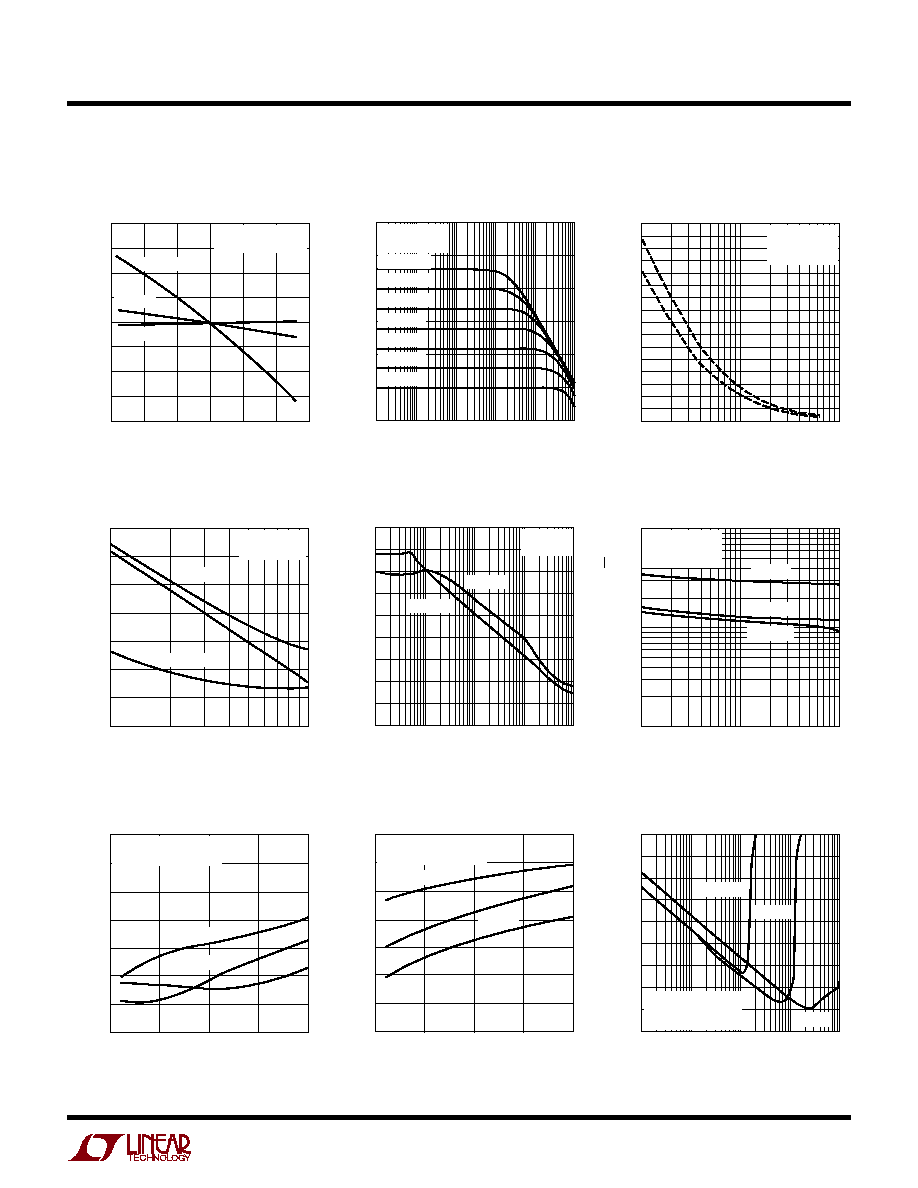
TYPICAL PERFOR A CE CHARACTERISTICS
U
W
(LTC6911-1)
LTC6911-1 Gain Shift
vs Temperature
TEMPERATURE (
∞
C)
≠50
GAIN CHANGE (dB)
0
0.025
≠0.025
25
75
6911 G01
≠25
0
50
0.050
≠0.050
0.075
≠0.075
0.100
≠0.100
100
GAIN = 100
GAIN = 10
GAIN = 1
V
S
= 5V
OUTPUT UNLOADED
FREQUENCY (Hz)
10
GAIN (dB)
30
50
0
20
40
100
10k
100k
1M
10M
6911 G02
≠10
1k
GAIN OF 100 (DIGITAL INPUT 111)
GAIN OF 1 (DIGITAL INPUT 001)
GAIN OF 2 (DIGITAL INPUT 010)
GAIN OF 5 (DIGITAL INPUT 011)
GAIN OF 10 (DIGITAL INPUT 100)
GAIN OF 20 (DIGITAL INPUT 101)
GAIN OF 50 (DIGITAL INPUT 110)
V
S
= 10V, V
IN
= 5mV
RMS
GAIN
1
0
≠3dB FREQUENCY (MHz) 2.0
4.0
8.0
∑
∑
∑
∑
∑
7.5
7.0
6.5
5.5
5.0
4.5
3.5
3.0
2.5
1.5
1.0
0.5
10
100
6911 G03
6.0
V
IN
= 5mV
RMS
V
S
= 2.7V
V
S
=
±
5V
∑
∑
∑
∑
∑
∑
∑
∑
∑
∑
∑
LTC6911-1 Frequency Response
LTC6911-1 ≠3dB Bandwidth
vs Gain Setting
LTC6911-1 Channel Isolation
vs Frequency
LTC6911-1 Power Supply
Rejection vs Frequency
LTC6911-1 Noise Density
vs Frequency
FREQUENCY (Hz)
85
100
95
90
120
115
110
105
6911 G04
CHANNEL-TO-CHANNEL ISOLATION (dB)
100k
1M
GAIN = 100
GAIN = 1
GAIN = 10
V
S
= 5V
V
OUT
= 1V
RMS
FREQUENCY (Hz)
20
REJECTION (dB)
40
50
70
90
10k
100k
1M
10M
6911 G05
0
1k
60
30
10
80
+SUPPLY
≠SUPPLY
V
S
=
±
2.5V
GAIN = 1
FREQUENCY (Hz)
1k
1
VOLTAGE NOISE DENSITY (nV/
Hz)
10
100
10k
100k
6911 G06
GAIN = 1
GAIN = 10
GAIN = 100
V
S
=
±
2.5V
T
A
= 25
∞
C
INPUT REFERRED
LTC6911-1 Distortion vs Frequency
with Light Loading (R
L
= 10k)
LTC6911-1 THD + Noise
vs Input Voltage
FREQUENCY (Hz)
0
≠60
≠50
≠30
150k
6911 G07
≠70
≠80
50k
100k
200k
≠90
≠100
≠40
THD (AMPLITUDE BELOW FUNDAMENTAL) (dB)
V
S
=
±
2.5V
V
OUT
= 1V
RMS
(2.83V
P-P
)
GAIN = 1
GAIN = 10
GAIN = 100
LTC6911-1 Distortion vs Frequency
with Heavy Loading (R
L
= 500
)
INPUT VOLTAGE (V
P-P
)
≠90
THD + NOISE (dB)
≠70
≠60
≠40
≠20
1m
0.1
1
10
6911 G09
≠110
10n
≠50
≠80
≠100
≠30
f
IN
= 1kHz
V
S
=
±
5V
BW = 100Hz TO 22kHz
GAIN = 1
GAIN = 10
GAIN = 100
FREQUENCY (Hz)
0
≠60
≠50
≠30
150k
6911 G08
≠70
≠80
50k
100k
200k
≠90
≠100
≠40
THD (AMPLITUDE BELOW FUNDAMENTAL) (dB)
V
S
=
±
2.5V
V
OUT
= 1V
RMS
(2.83V
P-P
)
GAIN = 1
GAIN = 10
GAIN = 100
LTC6911-1/LTC6911-2
11
sn691112 691112fs
TYPICAL PERFOR A CE CHARACTERISTICS
U
W
(LTC6911-2)
LTC6911-2 Gain Shift
vs Temperature
LTC6911-2 Frequency Response
LTC6911-2 ≠3dB Bandwidth
vs Gain Setting
LTC6911-2 Channel Isolation
vs Frequency
LTC6911-2 Power Supply
Rejection vs Frequency
LTC6911-2 Noise Density
vs Frequency
LTC6911-2 Distortion vs Frequency
with Light Loading (R
L
= 10k)
LTC6911-2 THD + Noise
vs Input Voltage
LTC6911-2 Distortion vs Frequency
with Heavy Loading (R
L
= 500
)
TEMPERATURE (
∞
C)
≠50
GAIN CHANGE (dB)
0
0.025
≠0.025
25
75
≠25
0
50
0.050
≠0.050
0.075
≠0.075
0.100
≠0.100
100
GAIN = 64
GAIN = 8
GAIN = 1
V
S
= 5V
OUTPUT UNLOADED
6911 G010
FREQUENCY (Hz)
10
GAIN (dB)
30
50
0
20
40
100
1k
100k
1M
10M
6911 G11
≠10
10k
V
S
=
±
5V
V
IN
= 10mV
RMS
GAIN OF 64
GAIN OF 32
GAIN OF 16
GAIN OF 4
GAIN OF 8
GAIN OF 2
GAIN OF 1
GAIN
1
0
≠3dB FREQUENCY (MHz) 2.0
4.0
8.0
7.5
7.0
6.5
5.5
5.0
4.5
3.5
3.0
2.5
1.5
1.0
0.5
10
100
6911 G12
6.0
V
IN
= 10mV
RMS
V
S
= 2.7V
V
S
=
±
5V
∑
∑
∑
∑
∑
∑
∑
∑
∑
∑
∑
∑
∑
∑
∑
∑
FREQUENCY (Hz)
85
100
95
90
120
115
110
105
6911 G13
CHANNEL-TO-CHANNEL ISOLATION (dB)
100k
1M
GAIN = 64
GAIN = 1
GAIN = 8
V
S
= 5V
V
OUT
= 1V
RMS
FREQUENCY (Hz)
20
REJECTION (dB)
40
50
70
90
10k
100k
1M
10M
6911 G14
0
1k
60
30
10
80
+SUPPLY
≠SUPPLY
V
S
=
±
2.5V
GAIN = 1
FREQUENCY (Hz)
1k
1
VOLTAGE NOISE DENSITY (nV/
Hz)
10
100
10k
100k
6911 G15
GAIN = 1
GAIN = 8
GAIN = 64
V
S
=
±
2.5V
T
A
= 25
∞
C
INPUT REFERRED
FREQUENCY (Hz)
0
≠60
≠50
≠30
150k
6911 G16
≠70
≠80
50k
100k
200k
≠90
≠100
≠40
THD (AMPLITUDE BELOW FUNDAMENTAL) (dB)
V
S
=
±
2.5V
V
OUT
= 1V
RMS
(2.83V
P-P
)
GAIN = 1
GAIN = 8
GAIN = 64
FREQUENCY (Hz)
0
≠60
≠50
≠30
150k
6911 G17
≠70
≠80
50k
100k
200k
≠90
≠100
≠40
THD (AMPLITUDE BELOW FUNDAMENTAL) (dB)
V
S
=
±
2.5V
V
OUT
= 1V
RMS
(2.83V
P-P
)
GAIN = 1
GAIN = 8
GAIN = 64
INPUT VOLTAGE (V
P-P
)
≠90
THD + NOISE (dB)
≠70
≠60
≠40
≠20
1m
0.1
1
10
6911 G18
≠110
10n
≠50
≠80
≠100
≠30
f
IN
= 1kHz
V
S
=
±
5V
BW = 100Hz TO 22kHz
GAIN = 1
GAIN = 8
GAIN = 64

LTC6911-1/LTC6911-2
12
sn691112 691112fs
U
U
U
PI FU CTIO S
INA (Pin 1): Analog Input. The input signal to the A channel
amplifier of the LTC6911-X is the voltage difference be-
tween the INA and AGND pin. The INA pin connects
internally to a digitally controlled resistance whose other
end is a current summing point at the same potential as the
AGND pin (Figure 1). At unity gain (digital input 001), the
value of this input resistance is approximately 10k
and
the INA pin voltage range is rail-to-rail (V
+
to V
≠
). At gain
settings above unity, the input resistance falls. The linear
input range at INA also falls inversely proportional to the
programmed gain. Tables 1 and 2 summarize this behav-
ior. The higher gains are designed to boost lower level
signals with good noise performance. In the "zero" gain
state (digital input 000), analog switches disconnect the
INA pin internally and this pin presents a very high input
resistance. The input may vary from rail to rail in the "zero"
gain setting, but the output is insensitive to it and is forced
to the AGND potential.
Circuitry driving the INA pin must consider the LTC6911-X's
input resistance, its lot-to-lot variance, and the variation of
this resistance from gain setting to gain setting. Signal
sources with significant output resistance may introduce
a gain error as the source's output resistance and the
LTC6911-X's input resistance form a voltage divider. This
is especially true at higher gain settings where the input
resistance is the lowest.
In single supply voltage applications, it is important to
remember that the LTC6911-X's DC ground reference for
both input and output is AGND, not V
≠
. With increasing
gains, the LTC6911-X's input voltage range for an unclipped
output is no longer rail-to-rail but diminishes inversely to
gain, centered about the AGND potential.
Figure 1. Block Diagram
≠
+
INPUT R ARRAY
FEEDBACK R ARRAY
OUTA
MOS-INPUT
OP AMP
MOS-INPUT
OP AMP
INA
G1
G2
G0
10
V
≠
9
V
+
691112 F01
7
≠
+
OUTB
8
1
INPUT R ARRAY
FEEDBACK R ARRAY
INB
3
AGND
V
+
V
≠
10k
10k
2
CMOS LOGIC
5
6
4

LTC6911-1/LTC6911-2
13
sn691112 691112fs
AGND (Pin 2): Analog Ground. The AGND pin is at the
midpoint of an internal resistive voltage divider, develop-
ing a potential halfway between the V
+
and V
≠
pins, with an
equivalent series resistance to the pin of nominally 5k
(Figure 1). AGND is also the noninverting input to both the
internal channel A and channel B amplifiers. This makes
AGND the ground reference voltage for the INA, INB, OUTA
and OUTB pins. Recommended analog ground plane con-
nection depends on how power is applied to the LTC6911-X
(see Figures 2, 3 and 4). Single power supply applications
typically use V
≠
for the system signal ground. The analog
ground plane in single supply applications should there-
fore tie to V
≠
, and the AGND pin should be bypassed to this
ground plane by a high quality capacitor of at least 1
µ
F
(Figure 2). The AGND pin provides an internal analog
reference voltage at half the V
+
supply voltage. Dual supply
applications with symmetrical supplies (such as
±
5V)
have a natural system ground plane potential of zero volts,
which can be tied directly to the AGND pin, making the zero
volt ground plane the input and output reference voltage
for the LTC6911-X (Figure 3). Finally, if dual asymmetrical
power supplies are used, the supply ground is still the
natural ground plane voltage. To maximize signal swing
U
U
U
PI FU CTIO S
capability with an asymmetrical supply, however, it is
often desirable to refer the LTC6911-X's analog input and
output to a voltage equidistant from the two supply rails V
+
and V
≠
. The AGND pin will provide such a potential when
open-circuited and bypassed with a capacitor (Figure 4).
Figure 3. Dual Supply Ground Plane Connection
Figure 2. Single Supply Ground Plane Connection
LTC6911-X
DIGITAL GROUND PLANE
(IF ANY)
ANALOG
GROUND
PLANE
1
SINGLE-POINT
SYSTEM GROUND
2
3
4
5
691112 F03
10
9
8
7
6
0.1
µ
F
V
≠
V
+
0.1
µ
F
Figure 4. Asymmetrical Dual Supply Ground Plane Connection
LTC6911-X
DIGITAL GROUND PLANE
(IF ANY)
ANALOG
GROUND
PLANE
1
SINGLE-POINT
SYSTEM GROUND
2
3
4
5
691112 F04
10
9
8
7
6
0.1
µ
F
V
≠
V
+
0.1
µ
F
1
µ
F
REFERENCE
V
+
+ V
≠
2
DIGITAL GROUND PLANE
(IF ANY)
ANALOG
GROUND
PLANE
SINGLE-POINT
SYSTEM GROUND
REFERENCE
V
+
2
691112 F02
1
µ
F
LTC6911-X
1
2
3
4
5
10
9
8
7
6
V
+
0.1
µ
F

LTC6911-1/LTC6911-2
14
sn691112 691112fs
U
U
U
PI FU CTIO S
In noise sensitive applications where AGND does not
directly tie to a ground plane, as in Figures 2 and 4, it is
important to AC-bypass the AGND pin. Otherwise, chan-
nel-to-channel isolation is degraded and wideband noise
will enter the signal path from the thermal noise of the
internal voltage divider resistors that present a ThÈvenin
equivalent resistance of approximately 5k
. This noise
can reduce SNR by at least 3dB at high gain settings. An
external capacitor from AGND to the ground plane, whose
impedance is well below 5k
at frequencies of interest,
will filter and suppress this noise. A 1
µ
F high quality
capacitor is effective for frequencies down to 1kHz. Larger
capacitors extend this suppression to lower frequencies.
This issue does not arise in dual supply applications
because the AGND pin ties directly to ground.
In applications requiring an analog ground reference other
than half the total supply voltage, the user can override the
built-in analog ground reference by tying the AGND pin to
a reference voltage within the AGND voltage range speci-
fied in the Electrical Characteristics table. The AGND pin
will load the external reference with approximately 5k
returned to the half-supply potential. AGND should still be
capacitively bypassed to a ground plane as noted above.
Do not connect the AGND pin to the V
≠
pin.
INB (Pin 3): Analog Input. Refer to INA pin description.
G0, G1, G2 (Pins 4, 5, 6): CMOS-Level Digital Gain
Control Inputs. G2 is the most significant bit (MSB) and G0
is the least significant bit (LSB). These pins control the
voltage gain settings for both channels (see Tables 1
and 2). Each channel's gain cannot be set independent of
the other channel. The logic input pins (G pins) are allowed
to swing from V
≠
to 10.5V above V
≠
, regardless of V
+
so
long as the logic levels meet the minimum requirements
specified in the Electrical Characteristics table. The G0, G1
and G2 pins are high impedance CMOS logic inputs, but
have small pull-down current sources (<10
µ
A) which will
force both channels into the "zero" gain state (digital input
000) if the logic inputs are externally floated. No speed
limitation is associated with the digital logic because it is
memoryless and much faster than the analog signal path.
V
≠
, V
+
(Pins 7, 9): Power Supply Pins. The V
+
and V
≠
pins
should be bypassed with 0.1
µ
F capacitors to an adequate
analog ground plane using the shortest possible wiring.
Electrically clean supplies and a low impedance ground
are important for the high dynamic range available from
the LTC6911-X (see further details under the AGND pin
description). Low noise linear power supplies are recom-
mended. Switching power supplies require special care to
prevent switching noise coupling into the signal path,
reducing dynamic range.
OUTB (Pin 8): Analog Output. This is the output of the B
channel internal operational amplifier and can swing rail-
to-rail (V
+
to V
≠
) as specified in the Electrical Characteris-
tics table. The internal op amp remains active at all times,
including the zero gain setting (digital input 000). For best
performance, loading the output as lightly as possible will
minimize signal distortion and gain error. The Electrical
Characteristics table shows performance at output cur-
rents up to 10mA, and the current limits which occur when
the output is shorted to mid-supply at 2.7V and
±
5V
supplies. Signal outputs above 10mA are possible but
current-limiting circuitry will begin to affect amplifier
performance at approximately 20mA. Long-term opera-
tion above 20mA output is not recommended. Do not
exceed a maximum junction temperature of 150
∞
C. The
output will drive capacitive loads up to 50pF. Capacitances
higher than 50pF should be isolated by a series resistor to
preserve AC stability.
OUTA (Pin 10): Analog Output. Refer to OUTB pin
description.

LTC6911-1/LTC6911-2
15
sn691112 691112fs
APPLICATIO S I FOR ATIO
W
U
U
U
Functional Description
The LTC6911-1/LTC6911-2 are small outline, wideband
inverting 2-channel amplifiers whose voltage gain is digi-
tally programmable. Each delivers a choice of eight volt-
age gains, controlled by the 3-bit digital parallel interface
(G pins), which accept CMOS logic levels. The gain code
is always monotonic; an increase in the 3-bit binary
number (G2 G1 G0) causes an increase in the gain. Tables
1 and 2 list the nominal voltage gains for LTC6911-1 and
LTC6911-2 respectively. Gain control within each ampli-
fier occurs by switching resistors from a matched array in
or out of a closed-loop op amp circuit using MOS analog
switches (Figure 1). Bandwidth depends on gain setting.
Curves in the Typical Performance Characteristics section
show measured frequency responses.
Digital Control
Logic levels for the LTC6911-X digital gain control inputs
(Pins 4, 5, 6) are nominally rail-to-rail CMOS, but can
swing above V
+
so long as the positive swing does not
exceed 10.5V with respect to V
≠
. Each logic input has a
small pull-down current source which can sink up to 10
µ
A
and is used to force the part into a gain of "zero" if the logic
inputs are left unconnected. A logic 1 is nominally V
+
. A
logic 0 is nominally V
≠
or alternatively, 0V when using
±
5V
supplies. The parts are tested with the values listed in the
Electrical Characteristics table. Digital Input "High" and
"Low" voltages are 10% and 90% of the nominal full
excursion on the inputs. That is, the tested logic levels are
0.27V and 2.43V with a 2.7V supply, 0.5V and 4.5V with a
5V supply, and 0.5V and 4.5V with
±
5V supplies. Do not
attempt to drive the digital inputs with TTL logic levels. TTL
logic sources should be adapted with suitable pull-up
resistors to V
+
keeping in mind the internal pull-down
current sources so that for a logic 1 they will swing to the
positive rail.
Timing Constraints
Settling time in the CMOS gain-control logic is typically
several nanoseconds and is faster than the analog signal
path. When amplifier gain changes, the limiting timing is
analog, not digital, because the effects of digital input
changes are observed only through the analog output
(Figure 1). The LTC6911-X's logic is static (not latched)
and therefore lacks bus timing requirements. However, as
with any programmable-gain amplifier, each gain change
causes an output transient as the amplifier's output moves,
with finite speed, toward a differently scaled version of the
input signal. Varying the gain faster than the output can
settle produces a garbled output signal. The LTC6911-X
analog path settles with a characteristic time constant or
time scale,
, that is roughly the standard value for a first
order band limited response:
= 0.35/(2
f
≠3dB
)
See the ≠3dB BW vs Gain Setting graph in the Typical
Performance Characteristics.
Offset Voltage vs Gain Setting
The Electrical Characteristics table lists DC gain depen-
dent voltage offset error in two gain configurations. The
voltage offsets listed, V
OS(IN)
, are referred to the input pin
(INA or INB). These offsets are directly related to the
internal amplifier input voltage offset, V
OS(OA)
, by the
magnitude of programmed gain, G:
V
V
G
G
OS OA
OS IN
(
)
( )
=
+
1
The input referred offset, V
OS(IN)
, for any gain setting can
be inferred from V
OS(OA)
and the gain magnitude, G. For
example, an internal offset V
OS(OA)
of 1mV will appear
referred to the INA and INB pins as 2mV at a gain setting

LTC6911-1/LTC6911-2
16
sn691112 691112fs
APPLICATIO S I FOR ATIO
W
U
U
U
of 1, or 1.5mV at a gain setting of 2. At high gains, V
OS(IN)
approaches V
OS(OA)
. (Offset voltage is random and can
have either polarity centered on 0V.) The MOS input
circuitry of the internal op amp in Figure 1 draws negligible
input currents (unlike some op amps), so only V
OS(OA)
and
G affect the overall amplifier's offset.
AC-Coupled Operation
Adding capacitors in series with the INA and INB pins
convert the LTC6911-X into a dual AC-coupled inverting
amplifier, suppressing the input signal's DC level (and also
adding the additional benefit of reducing the offset voltage
from the LTC6911-X's amplifier itself). No further compo-
nents are required because the input of the LTC6911-X
biases itself correctly when a series capacitor is added.
The INA and INB analog input pins connect internally to a
resistor whose nominal value varies between 10k and 1k
depending on the version of LTC6911 used (see the
rightmost column of Tables 1 and 2). Therefore, the low
frequency cutoff will vary with capacitor and gain setting.
For example, if a low frequency corner of 1kHz or lower on
the LTC6911-1 is desired, use a series capacitor of 0.16
µ
F
or larger. A 0.16
µ
F capacitor has a reactance of 1k
at
1kHz, giving a 1kHz lower ≠3dB frequency for gain settings
of 10V/V through 100V/V. If the LTC6911-1 is operated at
lower gain settings with an 0.16
µ
F capacitor, the higher
input resistance will reduce the lower corner frequency
down to 100Hz at a gain setting of 1V/V. These frequencies
scale inversely with the value of the input capacitor used.
Note that operating the LTC6911 family in "zero" gain
mode (digital inputs 000) open circuits the INA and INB
pins and this demands some care if employed with a series
AC-coupled input capacitor. When the chip enters the zero
gain mode, the opened INA or INB pin tends to sample and
freeze the voltage across the capacitor to the value it held
just before the zero gain state. This can place the INA or
INB pin at or near the DC potential of a supply rail (the INA
or INB pin may also drift to a supply potential in this state
due to small junction leakage currents). To prevent driving
the INA or INB pin outside the supply limit and potentially
damaging the chip, avoid AC input signals in the zero gain
state with an AC-coupled capacitor. Also, switching later
to a nonzero gain value will cause a transient pulse at the
output of the LTC6911-1 (with a time constant set by the
capacitor value and the new LTC6911-1 input resistance
value). This occurs because the INA and INB pins return to
the AGND potential forcing transient current sourced by
the amplifier output to charge the AC-coupling capacitor to
its proper DC blocking value.
SNR and Dynamic Range
The term "dynamic range" is much used (and abused)
with signal paths. Signal-to-noise ratio (SNR) is an unam-
biguous comparison of signal and noise levels, measured
in the same way and under the same operating conditions.
In a variable gain amplifier, however, further characteriza-
tion is useful because both noise and maximum signal
level in the amplifier will vary with the gain setting, in
general. In the LTC6911-X, maximum output signal is
independent of gain (and is near the full power supply
voltage, as detailed in the Swing sections of the Electrical
Characteristics table). The maximum input level falls with
increasing gain, and the input-referred noise falls as well
(as also listed in the table). To summarize the useful signal
range in such an amplifier, we define Dynamic Range (DR)
as the ratio of maximum input (at unity gain) to minimum
input-referred noise (at maximum gain). This DR has a
physical interpretation as the range of signal levels that
will experience an SNR above unity V/V or 0dB. At a 10V
total power supply, DR in the LTC6911-X (gains 0V/V to
100V/V) is typically 120dB (the ratio of a nominal 9.9V
P-P
,
or 3.5V
RMS
(maximum input), to the 3.8
µ
V
RMS
(high gain
input noise). The SNR of an amplifier is the ratio of input
level to input-referred noise, and can be 110dB with the
LTC6911 family at unity gain.

LTC6911-1/LTC6911-2
17
sn691112 691112fs
Construction and Instrumentation Cautions
Electrically clean construction is important in applications
seeking the full dynamic range of the LTC6911 family of
dual amplifiers. It is absolutely critical to have AGND either
AC bypassed or wired directly, using the shortest possible
wiring, to a low impedance ground return for best channel-
to-channel isolation. Short, direct wiring will minimize
parasitic capacitance and inductance. High quality supply
bypass capacitors of 0.1
µ
F near the chip provide good
decoupling from a clean, low inductance power source.
But several cm of wire (i.e., a few microhenrys of induc-
tance) from the power supplies, unless decoupled by
substantial capacitance (>10
µ
F) near the chip, can create
a high-Q LC resonance in the hundreds of kHz in the chip's
supplies or ground reference. This may impair circuit
performance at those frequencies. A compact, carefully
laid out printed circuit board with a good ground plane
makes a significant difference in minimizing distortion and
maximizing channel isolation. Finally, equipment to mea-
sure amplifier performance can itself add to distortion or
noise floors. Checking for these limits with wired shorts
from INA to OUTA and INB to OUTB in place of the chip is
a prudent routine procedure.
APPLICATIO S I FOR ATIO
W
U
U
U

LTC6911-1/LTC6911-2
18
sn691112 691112fs
Figure 5. Expanding a Dual Channel ADC's Dynamic Range
Expanding an ADC's Dynamic Range
Figure 5 shows a compact 2-channel data acquisition
system for wide ranging input levels. This figure combines
an LTC6911-X programmable amplifier (10-lead MSOP)
with an LTC1865 analog-to-digital converter (ADC) in an
8-lead MSOP. This ADC has 16-bit resolution and a
maximum sampling rate of 250ksps. An LTC6911-1, for
example, expands the ADC's input amplitude range by
40dB while operating from the same single 5V supply. The
499
resistor and 270pF capacitor couple cleanly be-
tween the LTC6911-X's output and the switched-capacitor
inputs of the LTC1865.
U
TYPICAL APPLICATIO
LTC6911-X
10
499
270pF
499
7
9
8
1
V
INA
AGND
V
INB
3
2
1
µ
F
270pF
0.1
µ
F
V
+
4
5
GAIN CONTROL
ADC INTERFACE
6
691112 F05
0.1
µ
F
V
+
691112 F05
CH0
CONV
SDI
SDO
SCK
V
CC
LTC1865
GND
CH1

LTC6911-1/LTC6911-2
19
sn691112 691112fs
U
PACKAGE DESCRIPTIO
MS Package
10-Lead Plastic MSOP
(Reference LTC DWG # 05-08-1661)
MSOP (MS) 0603
0.53
±
0.152
(.021
±
.006)
SEATING
PLANE
0.18
(.007)
1.10
(.043)
MAX
0.17 ≠ 0.27
(.007 ≠ .011)
TYP
0.127
±
0.076
(.005
±
.003)
0.86
(.034)
REF
0.50
(.0197)
BSC
1 2 3 4 5
4.90
±
0.152
(.193
±
.006)
0.497
±
0.076
(.0196
±
.003)
REF
8
9
10
7 6
3.00
±
0.102
(.118
±
.004)
(NOTE 3)
3.00
±
0.102
(.118
±
.004)
(NOTE 4)
NOTE:
1. DIMENSIONS IN MILLIMETER/(INCH)
2. DRAWING NOT TO SCALE
3. DIMENSION DOES NOT INCLUDE MOLD FLASH, PROTRUSIONS OR GATE BURRS.
MOLD FLASH, PROTRUSIONS OR GATE BURRS SHALL NOT EXCEED 0.152mm (.006") PER SIDE
4. DIMENSION DOES NOT INCLUDE INTERLEAD FLASH OR PROTRUSIONS.
INTERLEAD FLASH OR PROTRUSIONS SHALL NOT EXCEED 0.152mm (.006") PER SIDE
5. LEAD COPLANARITY (BOTTOM OF LEADS AFTER FORMING) SHALL BE 0.102mm (.004") MAX
0.254
(.010)
0
∞
≠ 6
∞
TYP
DETAIL "A"
DETAIL "A"
GAUGE PLANE
5.23
(.206)
MIN
3.20 ≠ 3.45
(.126 ≠ .136)
0.889
±
0.127
(.035
±
.005)
RECOMMENDED SOLDER PAD LAYOUT
0.305
±
0.038
(.0120
±
.0015)
TYP
0.50
(.0197)
BSC
Information furnished by Linear Technology Corporation is believed to be accurate and reliable.
However, no responsibility is assumed for its use. Linear Technology Corporation makes no represen-
tation that the interconnection of its circuits as described herein will not infringe on existing patent rights.

LTC6911-1/LTC6911-2
20
sn691112 691112fs
Linear Technology Corporation
1630 McCarthy Blvd., Milpitas, CA 95035-7417
(408) 432-1900
q
FAX: (408) 434-0507
q
www.linear.com
©
LINEAR TECHNOLOGY CORPORATION 2004
LT/TP 0104 1K ∑ PRINTED IN USA
RELATED PARTS
PART NUMBER
DESCRIPTION
COMMENTS
LT
Æ
1228
100MHz Gain Controlled Transconductance Amplifier
Differential Input, Continuous Analog Gain Control
LT1251/LT1256
40MHz Video Fader and Gain Controlled Amplifier
Two Input, One Output, Continuous Analog Gain Control
LTC1564
10kHz to 150kHz Digitally Controlled Filter and PGA
Continuous Time, Low Noise 8th Order Filter and 4-Bit PGA
LTC6910
Digitally Controlled Programmable Gain Amplifier in SOT-23
Single Channel Version of the LTC6911
LTC6915
Digitally Controlled Programmable Instrumentation
14 Bits of Gain Control
Amplifier with SPI Interface
TYPICAL APPLICATIO
U
Fully Differential Amplifier with Digitally Programmable Gain
1
2
3
4
5
10
9
8
7
6
LTC6911-1
OR
LTC6911-2
G0 G1
DIGITAL GAIN CONTROL
High Dynamic Range (PGA Input)
High CMRR (Differential Input)
G2
G0 G1
DIGITAL GAIN CONTROL
G2
1
2
3
4
8
7
6
5
8
7
6
5
LTC1992-1
OR
LTC1992-2
OR
LTC1992-5
OR
LTC1992-10
1
2
3
4
5
10
9
8
7
6
LTC6911-1
OR
LTC6911-2
1
2
3
4
LTC1992-1
OR
LTC1992-2
OR
LTC1992-5
OR
LTC1992-10
0.1
µ
F
0.1
µ
F
0.1
µ
F
0.1
µ
F
V
OUT
+
V
OUT
≠
5V
V
IN
+
V
IN
≠
V
IN
+
V
IN
≠
≠5V
0.1
µ
F
691112 TA03
V
OUT
+
V
OUT
≠
5V
0.1
µ
F
≠5V
0.1
µ
F
5V
≠5V
0.1
µ
F
≠5V