 | –≠–ª–µ–∫—Ç—Ä–æ–Ω–Ω—ã–π –∫–æ–º–ø–æ–Ω–µ–Ω—Ç: LTC7543 | –°–∫–∞—á–∞—Ç—å:  PDF PDF  ZIP ZIP |

1
LTC7543/LTC8143
Improved Industry Standard
Serial 12-Bit Multiplying DACs
s
Improved Direct Replacement for AD7543
and DAC-8143
s
Low Cost
s
DNL and INL Over Temperature:
±
0.5LSB
s
Easy, Fast and Flexible Serial Interface
s
Daisy-Chain 3-Wire Interface for Multiple DAC
Systems (LTC8143)
s
1LSB Maximum Gain Error Over Temperature
Eliminates Adjustment
s
Asynchronous Clear Input for Initialization
s
Four-Quadrant Multiplication
s
Low Power Consumption
s
16-Pin PDIP and SO Packages
The LTC
Æ
7543/LTC8143 are serial-input 12-bit multiply-
ing digital-to-analog converters (DACs). They are superior
pin compatible replacements for the AD7543 and
DAC-8143. Improvements include better accuracy, better
stability over temperature and supply variations, lower
sensitivity to output amplifier offset, tighter timing speci-
fications and lower output capacitance.
An easy-to-use serial interface includes an asynchronous
CLEAR input for systems requiring initialization to a known
state. The LTC8143 has a serial data output to allow daisy-
chaining multiple DACs on a 3-wire interface bus.
These DACs are extremely versatile. They can be used for
2-quadrant and 4-quadrant multiplying, programmable
gain and single supply applications, such as noninverting
voltage output and biased or offset ground mode.
Parts are available in 16-pin PDIP and SO packages and
are specified over the extended industrial temperature
range, ≠ 40
∞
C to 85
∞
C.
FEATURES
DESCRIPTIO
N
U
s
Process Control and Industrial Automation
s
Remote Microprocessor-Controlled Systems
s
Digitally Controlled Filters and Power Supplies
s
Programmable Gain Amplifiers
s
Automatic Test Equipment
APPLICATIO
N
S
U
, LTC and LT are registered trademarks of Linear Technology Corporation.
TYPICAL APPLICATIO
N
U
Multiplying DAC Has Easy 3-Wire Serial Interface
V
DD
V
REF
LTC7543
LTC8143
R
FB
AGND
DGND
3
12
4
7
5
2
14
5V
V
IN
CLOCK
DATA
LOAD
STB1
SRI
LD1
15
16
1
OUT 1
33pF
V
OUT
7543/8143 TA01
OUT 2
≠
+
LT
Æ
1097
Integral Nonlinearity Over Temperature
DIGITAL INPUT CODE
0
INTEGRAL NONLINEARITY (LSB)
4095
7543/8143 TA02
1024
2048
3072
1.0
0.5
0
≠0.5
≠1.0
512
1536
2560
3584
T
A
= 85
∞
C
T
A
= 25
∞
C
T
A
= ≠40
∞
C

2
LTC7543/LTC8143
ABSOLUTE
M
AXI
M
U
M
RATINGS
W
W
W
U
PACKAGE/ORDER I
N
FOR
M
ATIO
N
W
U
U
V
DD
to AGND .............................................. ≠ 0.5V to 7V
V
DD
to DGND .............................................. ≠ 0.5V to 7V
AGND to DGND ............................................ V
DD
+ 0.5V
DGND to AGND ............................................ V
DD
+ 0.5V
Digital Inputs to DGND ............... ≠ 0.5V to (V
DD
+ 0.5V)
V
OUT1
, V
OUT2
to AGND ................. ≠ 0.5V to (V
DD
+ 0.5V)
V
REF
to AGND, DGND ............................................
±
25V
V
RFB
to AGND, DGND ...........................................
±
25V
Maximum Junction Temperature .......................... 150
∞
C
Operating Temperature Range ............... ≠ 40
∞
C to 85
∞
C
Storage Temperature Range ................ ≠ 65
∞
C to 150
∞
C
Lead Temperature (Soldering, 10 sec).................. 300
∞
C
LTC7543GKN
LTC7543KN
LTC7543GKSW
LTC7543KSW
LTC8143EN
LTC8143FN
LTC8143ESW
LTC8143FSW
ORDER PART
NUMBER
Consult factory for Military grade parts.
T
JMAX
= 150
∞
C,
JA
= 100
∞
C/ W (N)
T
JMAX
= 150
∞
C,
JA
= 130
∞
C/ W (SW)
V
DD
= 5V, V
REF
= 10V, V
OUT1
= V
OUT2
= AGND = DGND =0V, T
A
= T
MIN
to T
MAX
, unless otherwise specified.
ACCURACY CHARACTERISTICS ≠
LTC7543GK
LTC7543K
SYMBOL PARAMETER
CONDITIONS
MIN
TYP
MAX
MIN
TYP
MAX
UNITS
Resolution
q
12
12
Bits
INL
Integral Nonlinearity
(Note 1)
q
±
0.5
±
0.5
LSB
(Relative Accuracy)
DNL
Differential Nonlinearity
Guaranteed Monotonic, T
MIN
to T
MAX
q
±
0.5
±
0.5
LSB
GE
Gain Error
(Note 2)
T
A
= 25
∞
C
±
1
±
2
LSB
T
MIN
to T
MAX
q
±
1
±
2
LSB
Gain Temperature Coefficient
(Note 3)
q
1
5
1
5
ppm/
∞
C
(
Gain/
Temp)
I
LKG
Output Leakage Current
(Note 4)
T
A
= 25
∞
C
±
1
±
1
nA
T
MIN
to T
MAX
q
±
10
±
10
nA
Zero-Scale Error
T
A
= 25
∞
C
±
0.006
±
0.006
LSB
T
MIN
to T
MAX
q
±
0.06
±
0.06
LSB
PSRR
Power Supply Rejection Ratio V
DD
= 5V
±
5%
q
±
0.0001
±
0.002
±
0.0001
±
0.002
%/%
1
2
3
4
5
6
7
8
TOP VIEW
SW PACKAGE
16-LEAD PLASTIC SO WIDE
N PACKAGE
16-LEAD PDIP
16
15
14
13
12
11
10
9
OUT 1
OUT 2
AGND
STB1
LD1
SRI
STB2
R
FB
V
REF
V
DD
CLR
DGND
STB4
STB3
LD2
NC (LTC7543)
SRO (LTC8143)
LTC7543
3
LTC7543/LTC8143
V
DD
= 5V, V
REF
= 10V, V
OUT1
= V
OUT2
= AGND = DGND = 0V, T
A
= T
MIN
to T
MAX
, unless otherwise specified.
LTC8143E
LTC8143F
SYMBOL PARAMETER
CONDITIONS
MIN
TYP
MAX
MIN
TYP
MAX
UNITS
Resolution
q
12
12
Bits
INL
Integral Nonlinearity
(Note 1)
q
±
0.5
±
1
LSB
(Relative Accuracy)
DNL
Differential Nonlinearity
Guaranteed Monotonic, T
MIN
to T
MAX
q
±
0.5
±
1
LSB
GE
Gain Error
(Note 2)
T
A
= 25
∞
C
±
1
±
2
LSB
T
MIN
to T
MAX
q
±
2
±
2
LSB
Gain Temperature Coefficient
(Note 3)
q
1
5
1
5
ppm/
∞
C
(
Gain/
Temp)
I
LKG
Output Leakage Current
(Note 4)
T
A
= 25
∞
C
±
5
±
5
nA
T
MIN
to T
MAX
q
±
25
±
25
nA
Zero-Scale Error
T
A
= 25
∞
C
±
0.03
±
0.03
LSB
T
MIN
to T
MAX
q
±
0.15
±
0.15
LSB
PSRR
Power Supply Rejection Ratio V
DD
= 5V
±
5%
q
±
0.0001
±
0.002
±
0.0001
±
0.002
%/%
ACCURACY CHARACTERISTICS ≠
LTC8143
V
DD
= 5V, V
REF
= 10V, V
OUT1
= V
OUT2
= AGND = DGND = 0V, T
A
= T
MIN
to T
MAX
, unless otherwise specified.
ELECTRICAL CHARACTERISTICS ≠
LTC7543/LTC8143
LTC7543/LTC8143
ALL GRADES
SYMBOL PARAMETER
CONDITIONS
MIN
TYP
MAX
UNITS
Reference Input
R
REF
V
REF
Input Resistance
(Note 5)
q
8
11
15
k
AC Performance (Note 3)
Output Current Settling Time
(Notes 6, 7)
q
0.25
1
µ
s
Multiplying Feedthrough Error
V
REF
=
±
10V, 10kHz Sinewave
q
0.8
2
mV
P-P
Digital-to-Analog Glitch Energy
(Notes 6, 8)
q
2
20
nV-sec
THD
Total Harmonic Distortion
(Note 9)
q
≠ 108
≠ 92
dB
Output Noise Voltage Density
(Note 10)
q
13
nV/
Hz
Analog Outputs (Note 3)
C
OUT
Output Capacitance
DAC Register Loaded to All 1s
C
OUT1
q
60
90
pF
C
OUT2
q
20
60
pF
DAC Register Loaded to All 0s
C
OUT1
q
30
60
pF
C
OUT2
q
50
90
pF
Digital Inputs
V
IH
Digital Input High Voltage
q
2.4
V
V
IL
Digital Input Low Voltage
q
0.8
V
I
IN
Digital Input Current
V
IN
= 0V to V
DD
q
0.001
±
1
µ
A
C
IN
Digital Input Capacitance
(Note 3), V
IN
= 0V
q
8
pF
Digital Outputs: SRO (LTC8143 Only)
V
OH
Digital Output High
I
OH
= ≠ 200
µ
A
q
4
V
V
OL
Digital Output Low
I
OL
= 1.6mA
q
0.4
V

4
LTC7543/LTC8143
V
DD
= 5V, V
REF
= 10V, V
OUT1
= V
OUT2
= AGND = DGND = 0V, T
A
= T
MIN
to T
MAX
, unless otherwise specified.
ELECTRICAL CHARACTERISTICS ≠
LTC7543/LTC8143
The
q
denotes specifications which apply over the full operating
temperature range.
Note 1:
±
0.5LSB =
±
0.012% of full scale.
Note 2: Using internal feedback resistor.
Note 3: Guaranteed by design, not subject to test.
Note 4: I
OUT1
with DAC register loaded with all 0s or I
OUT2
with DAC
register loaded with all 1s.
Note 5: Typical temperature coefficient is 100ppm/
∞
C.
Note 6: OUT 1 load = 100
in parallel with 13pF.
Note 7: To 0.01% for a full-scale change, measured from falling edge of
LD1 or LD2.
Note 8: V
REF
= 0V. DAC register contents changed from all 0s to all 1s or
from all 1s to all 0s.
Note 9: V
REF
= 6V
RMS
at 1kHz. DAC register loaded with all 1s.
Note 10: Calculation from e
n
=
4KTRB where: K = Boltzmann constant
(J/K
∞
); R = resistance (
); T = resistor temperature (
∞
K); B = bandwidth
(Hz).
Note 11: Minimum high time for STB1, STB2, STB4. Minimum low time
for STB3.
Note 12. Minimum low time for STB1, STB2, STB4. Minimum high time
for STB3.
LTC7543/LTC8143
ALL GRADES
SYMBOL
PARAMETER
CONDITIONS
MIN
TYP
MAX
UNITS
Timing Characteristics (Note 3)
t
DS1
Serial Input to Strobe Setup Time
STB1 Used as the Strobe
q
50
5
ns
t
DS2
STB2 Used as the Strobe
q
20
≠ 5
ns
t
DS3
STB3 Used as the Strobe
q
0
≠ 30
ns
t
DS4
STB4 Used as the Strobe
q
0
≠ 30
ns
t
DH1
Serial Input to Strobe Hold Time
STB1 Used as the Strobe
q
30
10
ns
t
DH2
STB2 Used as the Strobe
q
50
25
ns
t
DH3
STB3 Used as the Strobe
q
80
55
ns
t
DH4
STB4 Used as the Strobe
q
80
55
ns
t
SRI
Serial Input Data Pulse Width
q
80
ns
t
STB1
, t
STB2
, Strobe Pulse Width
(Note 11)
q
80
ns
t
STB3
, t
STB4
t
STB1
, t
STB2
, Strobe Pulse Width
(Note 12)
q
80
ns
t
STB3
, t
STB4
t
LD1
, t
LD2
Load Pulse Width
q
140
ns
t
ASB
LSB Strobed into Input Register
q
0
ns
to Load DAC Register Time
t
CLR
Clear Pulse Width
q
80
ns
SRO Timing Characteristics (LTC8143 Only)
t
PD
STB2, STB3, STB4 Strobe to SRO
C
L
= 50pF
q
220
120
ns
Propagation Delay
t
PD1
STB1 to SRO Propagation Delay
C
L
= 50pF
q
150
80
ns
Power Supply
V
DD
Supply Voltage
q
4.75
5
5.25
V
I
DD
Supply Current
Digital Inputs = 0V or V
DD
q
0.1
mA
Digital Inputs = V
IH
or V
IL
q
2
mA
(t
STB
= 80ns)
(t
STB
= 80ns)
5
LTC7543/LTC8143
40k
10k
40k
20k
40k
20k
40k
20k
40k
40k
40k
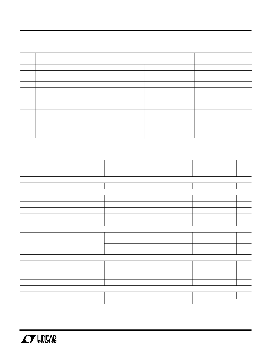
DECODER
BIT 1
(MSB)
BIT 2
BIT 3
BIT 4
BIT 12
(LSB)
CLR
CLK
OUT
SRO
LTC8143 ONLY
IN
LOAD
DGND
V
DD
V
REF
R
FB
OUT 1
OUT 2
SRI
7
AGND
3
2
1
16
7543/8143 BD
DAC REGISTER
INPUT 12-BIT SHIFT REGISTER
9
8
10
12
11
4
6
5
13
14
15
STB1
STB2
STB3
STB4
LD1
CLR
LD2
BLOCK DIAGRA
M
W
TI I G DIAGRA
U
W
W
SRI
SRO
(LTC8143 ONLY)
LD1, LD2
PREVIOUS
WORD
BIT 1
MSB
BIT 1 (MSB)
PREVIOUS WORD
BIT 1 (MSB)
CURRENT WORD
BIT 2
BIT 2
BIT 3
BIT 11
7543/8143 TD01
BIT 12
LSB
BIT 12
LSB
t
DS1
t
DS2
t
DS3
t
DS4
t
DH1
t
DH2
t
DH3
t
DH4
t
PD
t
PD1
t
STB1
t
STB2
t
STB3
t
STB4
t
SRI
t
ASB
t
STB1
t
STB2
t
STB3
t
STB4
t
LD1
t
LD2
STROBE INPUT
STB1, STB2, STB4
(INVERT FOR STB3)

6
LTC7543/LTC8143
TRUTH TABLES
Table 1. LTC7543/LTC8143 Input Register
CONTROL INPUTS
Input Register Operation
STB1 STB2 STB3 STB4
(LTC8143: SRO Operation)
0
1
0
Serial Data Bit on SRI Loaded into Input
0
1
0
Register, MSB First
0
0
0
(LTC8143: Data Bit or SRI Appears on
0
0
1
SRO Pin After 12 Clocked Bits)
1
X
X
X
No Input Register Operation
X
1
X
X
(LTC8143: No SRO Operation)
X
X
0
X
X
X
X
1
Table 2. LTC7543/LTC8143 DAC Register
CONTROL INPUTS
CLR
LD1
LD2
DAC Register Operation
0
X
X
Reset DAC Register to All 0s (Asynchronous
Operation; No Effect on Input Register)
1
1
X
No DAC Register Operation
1
X
1
1
0
0
Load DAC Register with the Contents of Input
Register
TYPICAL APPLICATIO
N
S
U
V
DD
V
REF
LTC7543
LTC8143
R
FB
AGND
DGND
3
12
10
4
7
5
6
9
8
11
2
14
13
5V
V
REF
≠10V TO 10V
TO NEXT DAC
FOR DAISY-CHAINING
(LTC8143)
15
16
1
OUT 1
33pF
0.1
µ
F
V
OUT
0V TO ≠V
REF
7543/8143 TA03
OUT 2
≠
+
LT1097
CLR
STB3
STB1
SRI
LD1
SRO (LTC8143)
LD2
STB2
STB4
µ
P
Unipolar Operation (2-Quadrant Multiplication)
DIGITAL INPUT
BINARY NUMBER IN
ANALOG OUTPUT
DAC REGISTER
V
OUT
MSB
LSB
1111
1111
1111
≠ V
REF
(4095/4096)
1000
0000
0000
≠ V
REF
(2048/4096) = ≠ V
REF
/2
0000
0000
0001
≠ V
REF
(1/4096)
0000
0000
0000
0V
Unipolar Binary Code Table

7
LTC7543/LTC8143
TYPICAL APPLICATIO
N
S
U
V
DD
V
REF
LTC7543
LTC8143
R
FB
R1
10k
R3
20k
R2
20k
AGND
DGND
3
12
2
14
5V
V
REF
≠10V TO 10V
15
16
1
OUT 1
0.1
µ
F
(LOGIC INPUTS
OMITTED FOR
CLARITY)
V
OUT
7543/8143 TA04
OUT 2
≠
+
1/2
LT1112
33pF
≠
+
1/2
LT 1112
Bipolar Operation (4-Quadrant Multiplication)
DIGITAL INPUT
BINARY NUMBER IN
ANALOG OUTPUT
DAC REGISTER
V
OUT
MSB
LSB
1111
1111
1111
V
REF
(2047/2048)
1000
0000
0001
V
REF
(1/2048)
1000
0000
0000
0V
0111
1111
1111
≠ V
REF
(1/2048)
0000
0000
0000
≠ V
REF
(2048/2048) = ≠ V
REF
Bipolar Offset Binary Code Table
Information furnished by Linear Technology Corporation is believed to be accurate and reliable.
However, no responsibility is assumed for its use. Linear Technology Corporation makes no represen-
tation that the interconnection of its circuits as described herein will not infringe on existing patent rights.

8
LTC7543/LTC8143
Linear Technology Corporation
1630 McCarthy Blvd., Milpitas, CA 95035-7487
(408) 432-1900
q
FAX
: (408) 434-0507
q
TELEX
: 499-3977
LT/GP 0695 10K ∑ PRINTED IN USA
©
LINEAR TECHNOLOGY CORPORATION 1995
PACKAGE DESCRIPTIO
N
U
Dimension in inches (millimeters) unless otherwise noted.
N Package
16-Lead Plastic DIP
N16 0694
0.255
±
0.015*
(6.477
±
0.381)
0.770*
(19.558)
MAX
16
1
2
3
4
5
6
7
8
9
10
11
12
13
14
15
0.015
(0.381)
MIN
0.125
(3.175)
MIN
0.130
±
0.005
(3.302
±
0.127)
0.065
(1.651)
TYP
0.045 ≠ 0.065
(1.143 ≠ 1.651)
0.018
±
0.003
(0.457
±
0.076)
0.045
±
0.015
(1.143
±
0.381)
0.100
±
0.010
(2.540
±
0.254)
0.009 ≠ 0.015
(0.229 ≠ 0.381)
0.300 ≠ 0.325
(7.620 ≠ 8.255)
0.325
+0.025
≠0.015
+0.635
≠0.381
8.255
(
)
*THESE DIMENSIONS DO NOT INCLUDE MOLD FLASH OR PROTRUSIONS.
MOLD FLASH OR PROTURSIONS SHALL NOT EXCEED 0.010 INCH (0.254mm).
S Package
16-Lead Plastic SOL
SOL16 0392
NOTE:
1. PIN 1 IDENT, NOTCH ON TOP AND CAVITIES ON THE BOTTOM OF PACKAGES ARE THE MANUFACTURING OPTIONS.
THE PART MAY BE SUPPLIED WITH OR WITHOUT ANY OF THE OPTIONS.
NOTE 1
0.398 ≠ 0.413
(10.109 ≠ 10.490)
(NOTE 2)
16
15
14
13
12
11
10
9
1
2
3
4
5
6
7
8
0.394 ≠ 0.419
(10.007 ≠ 10.643)
0.037 ≠ 0.045
(0.940 ≠ 1.143)
0.004 ≠ 0.012
(0.102 ≠ 0.305)
0.093 ≠ 0.104
(2.362 ≠ 2.642)
0.050
(1.270)
TYP
0.014 ≠ 0.019
(0.356 ≠ 0.482)
TYP
0
∞
≠ 8
∞
TYP
NOTE 1
0.005
(0.127)
RAD MIN
0.009 ≠ 0.013
(0.229 ≠ 0.330)
0.016 ≠ 0.050
(0.406 ≠ 1.270)
0.291 ≠ 0.299
(7.391 ≠ 7.595)
(NOTE 2)
◊
45
∞
0.010 ≠ 0.029
(0.254 ≠ 0.737)
2. THESE DIMENSIONS DO NOT INCLUDE MOLD FLASH OR PROTRUSIONS.
MOLD FLASH OR PROTRUSIONS SHALL NOT EXCEED 0.006 INCH (0.15mm).
RELATED PARTS
PART NUMBER
DESCRIPTION
COMMENTS
LTC1257
Complete Serial I/O V
OUT
12-Bit DAC
5V to 15V Single Supply in 8-Pin SO and PDIP
LTC1451/LTC1452/LTC1453
Complete Serial I/O V
OUT
12-Bit DACs
3V/5V Single Supply in 8-Pin SO and PDIP
LTC7541A
Parallel I/O Mulitplying 12-Bit DAC
12-Bit Wide Input
LTC8043
Serial Mulitplying 12-Bit DAC
8-Pin SO and PDIP