w w w . l i t t e l f u s e . c o m
2.0
B
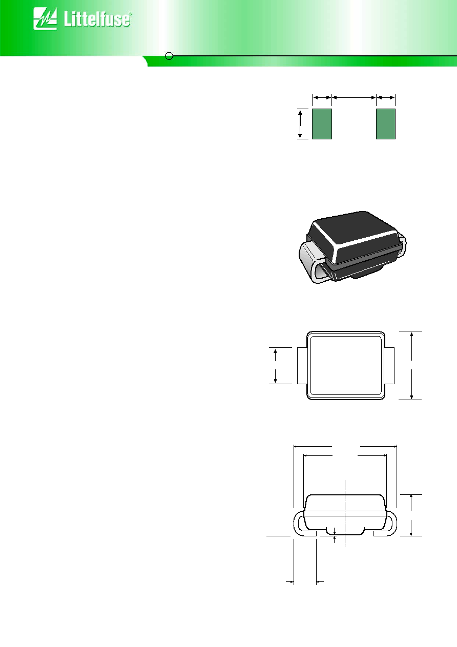
3.30/3.94
A
5.21/5.59
4.06/4.57
.102
.203
0.76/1.27
SEATING PLANE
2.18/2.44
2.26
2.16
2.74
2.16
FEATURES
G
Bi-directional transient voltage protection
G
Glass passivated junction
G
Nano second clamping response
G
Surge capability up to 250 (Amps)
G
No performance degradation under service life
G
Industry standard DO-2144AA Jedec outline
G
Available on tape (12mm)
G
UL recognised
MECHANICAL CHARACTERISTICS
G
Transfer molded, void free epoxy body
G
Terminals: modified `J' bend for large contact area
G
Tin/Lead plated leads
G
Maximum case temperature for soldering purposes: 230∞C for 10 seconds
G
Standard packaging: 12mm tape (meets EIA 481-1)
G
Device marking, device code, logo
59
All dimensions in mm
Solder Pads
SMTBJ SiBOD
TM
series

60
w w w . l i t t e l f u s e . c o m
SMTBJ SiBOD
TM
series
ELECTRICAL CHARACTERISTICS @ 25∞C Tamb
SYMBOL
V
RM
V
BR
V
BO
V
T
PARAMETER
Stand-off voltage
Breakdown voltage
Breakover voltage
On-state voltage
ABSOLUTE RATINGS
SYMBOL
Ipp
Itsm
di/dt
T stg
Tj
TL
PARAMETER
Peak Pulse Current
Non-repetitive surge peak on-state current
Critical rate of rise of on-state current
Storage and operating junction temperature range
Maximum temperature for soldering
(For period of 10 seconds max)
10/1000 µsec
8-20 µs expo
tp20 ms
Non-repetitive
Type A
50
150
Type B
100
250
All parameters are tested using Fet TestTM Model 3600.
Device
Type
SMTBJ050 A or B
SMTBJ070 A or B
SMTBJ100 A or B
SMTBJ120 A or B
SMTBJ170 A or B
SMTBJ200 A or B
Vrm
50
70
100
120
170
200
Irm
@ Vrm
(µA)
1
1
1
1
1
1
Vbr
MIN
60
80
110
140
180
220
Vbo
MAX
80
120
135
165
215
265
Vt
TYP
@ 1A
<2V
<2V
<2V
<2V
<2V
<2V
Ibo
TYP
(mA)
50
50
50
50
50
50
Ih
MIN
(mA)
150
150
150
150
150
150
I
RM
I
BO
I
H
Stand-off current
Breakover current
Holding current
30
100
-40 to +150
150
230
A
A
A
A/µs
∞C
∞C
∞C
VALUE