217
w w w . l i t t e l f u s e . c o m
5
TVS DIODE ARRA
YS
TVS Diode Arrays
Upstream USB Port Terminator with ESD Suppression & EMI Filtering
The Littelfuse SPUSB1 Series is a multifunctional USB port protection
network designed to provide ESD protection, EMI/RFI filtering and line
termination for a single USB 1.1 port. The SPUSB1 can replace a mini-
mum of ten typically larger "discrete" devices resulting in inventory and
placement cost savings.
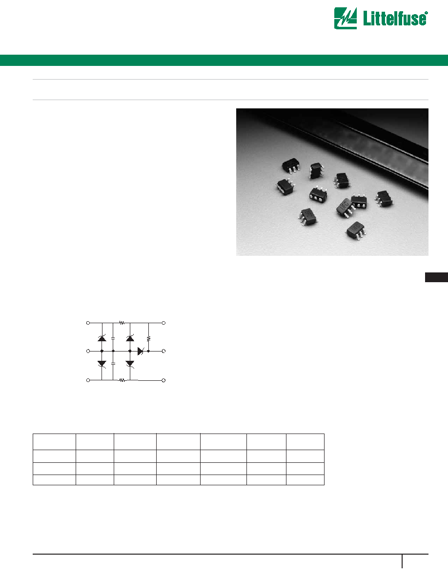
The SPUSB1 Series combines Transient Voltage Suppression (TVS)
avalanche diodes, EMI/RFI filtering components (R1 and C1), and
a1.5k
termination resistor (R2). The filtering components are included
to satisfy recommendations in the USB 1.1 specification, and the 1.5k
resistor (R2) is included as a pull-up resistor to VBUS.
The SPUSB1 Series can be used for termination and protection
of"upstream" USB devices such as PDAs, digital cameras, scanners and
hubs which are often at risk from transient voltage surges and
electromagnetic interference from both internal and external sources.
To support a wide range of circuit conditions, Littelfuse offers three
resistance values for the series resistor (R1). The series resistance plus
the USB driver output resistance must be close to the USB cable's char-
acteristic impedance of 45
(90
balanced) to minimize transmission
line reflections.
Circuit Diagram
Features
� One upstream USB port terminator, EMI filter and transient
overvoltage protector in a single surface-mount package
� Compact SC70 package saves board space and lowers
manufacturing costs compared to discrete solutions
� ESD protection to 30kV contact discharge per MIL-STD- 883D,
method 3015
� ESD protection to 15kV contact discharge per IEC 61000-4-2
international standard
Applications
� Desktop/Laptop PCs
� USB peripherals (printers, scanners, zip drives)
� PDAs / wireless handsets
� Digital cameras
� MP3 Players
� Cable Modems
Ordering Information
2
C1
GND
1
3
C1
5
6
4
R2
R1
R1
V BUS
SC70-6
DEVICE
BRAND
UFA
UFB
UFC
PKG
TYPE
SC70-6
SC70-6
SC70-6
#/REEL
3000
3000
3000
C1 (pF)
47
47
47
PART
NUMBER
SPUSB1AJT
SPUSB1BJT
SPUSB1CJT
R1 (Ohm)
12
22
33
R2 (KOhm)
1.5
1.5
1.5
SPUSB1 Series
218
w w w . l i t t e l f u s e . c o m
TVS Diode Arrays
SPUSB1 Series
Upstream USB Port Terminator with ESD Suppression & EMI Filtering
Absolute Maximum Ratings
Supply Voltage V
Parameter
Rating
Unit
BUS
DC Power per Resistor
Package Power
Temperature Range:
Operating
Storage
5.5
100
200
-40 to +85
-65 to +150
V
mW
mW
C
�
Resistance R1 (SPUSB1AJT only)
Parameter
Unit
Specifications
(at 25
�
C unless specified otherwise)
Resistance R1 (SPUSB1CJT only)
Resistance R1 (SPUSB1BJT only)
Resistance R2
Capacitance C1 @ 2.5 v DC, 1MHz
Diode Leakage at 3.3V
Diode Reverse Bias Stand-off Voltage, 1= 10
�
A
Signal Clamp Voltage:
Positive Clamp, 10mA
Negative Clamp, 10mA
In-system ESD Withstand Voltage
Human Body Model (MIL-STD-883D, method 3015
IEC 81000-4-2, contact discharge method (I/O pins)
IEC 81000-4-2, contact discharge method (V pin)
(1)
BUS
Clamping Voltage During ESD Discharge
MIL-STD-883D (Method 3015), 8kV
(1)
MAX
TYP
MIN
k
pF
nA
V
12
33
22
1.5
47
1
6%
26%
18%
1.2%
38%
5.5
14%
40%
26%
18%
56%
100
Positive
Negative
5.6
-1.2
6.8
-0.8
8.0
-0.4
V
V
�
30
�
15
�
25
kV
kV
kV
V
V
10
-5
Note:
(1) ESD applied to input/outputV pins with respect to GND, one at a time.
Clamping Voltage is measured at the opposite side of the EMI filter to the ESD pin (ie: if ESD is applied to pin1 then clamping
voltage is measured at pin 6). Unused pins are open.
These parameters guaranteed by design.
DD
Standard
2
C1
GND
D1
D2
D3
D4
1
3
C1
5
6
4
R2
3.3V
R1
R1
V BUS
D+
USB 1.1
CONNECTOR
D-
D+
USB 1.1
CONTROLLER
IC
D-
GND
2
C1
GND
D1
D2
D3
D4
1
3
C1
5
6
4
R2
3.3V
R1
R1
V BUS
D-
USB 1.1
CONNECTOR
D+
D-
USB 1.1
CONTROLLER
IC
D+
GND
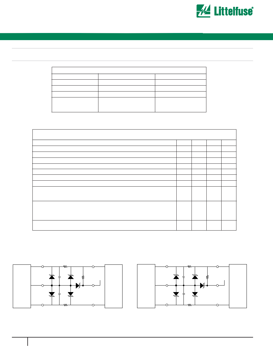
Figure 1. Full-Speed Devices (12Mbits per second)
For full speed operation the pull-up resistor R2 is connected to the D+ pin.
Figure 2. Low-Speed Devices (1.5Mbits per second)
Low speed connection requires the pull-up resistor R2 to be connected to the D-
pin. Please note the reversal of the D- and D+ pins on Figure 2 versus Figure 1.
APPLICATIONS INFORMATION

219
w w w . l i t t e l f u s e . c o m
5
TVS DIODE ARRA
YS
TVS Diode Arrays
Upstream USB Port Terminator with ESD Suppression & EMI Filtering
SPUSB1 Series
B
1
2
3
4
5
6
B
E
HE
c
L
A1
A
D
A2
B
Outline Drawings
SPUSB1AJT - SC70-6
SPUSB1BJT - SC70-6
SPUSB1CJT - SC70-6
Package
Pins
JEDEC
A
A1
A2
B
c
D
E
e
HE
L
SC70-6
6
MO-203 Issue A
mm
inches
min
max
min
max
0.80
1.10
0.031
0.043
0.00
0.10
0.000
0.004
0.70
1.00
0.028
0.039
0.15
0.30
0.006
0.012
0.08
0.25
0.003
0.010
1.85
2.25
0.073
0.089
1.15
1.35
0.045
0.053
2.00
2.40
0.26
0.46
0.65 BSC
0.026 BSC
0.079
0.094
0.010
0.018
P
D
@70
�
C
0.2W
# / bag
1000 pcs
# / tape & reel
3,000 pcs
*See device brand for marking information.
M
N
O
P
R
S
T
-
1.60
-
0.063
-
1.30
-
0.052
-
0.65
-
0.026
-
0.70
-
0.058
-
0.35
-
0.014
-
0.90
-
0.035
-
2.50
-
0.098
Recommended Pad Layout
P
T
+
+
+
+
+
+
+
S (REF)
N (REF)
M (REF)
O (REF)
R
Mechanical Specifications
Lead Plating
Tin-Lead
Lead Material
Copper Alloy
Lead Coplanarity
0.004 inches (0.102mm)
Subsitute Material
Silicon
Body Material
Molded Epoxy
Flammability UL94-V-0
PACKAGING INFORMATION