 | –≠–ª–µ–∫—Ç—Ä–æ–Ω–Ω—ã–π –∫–æ–º–ø–æ–Ω–µ–Ω—Ç: LS7031 | –°–∫–∞—á–∞—Ç—å:  PDF PDF  ZIP ZIP |

6 DECADE MOS UP COUNTER WITH 8 DECADE LATCH AND MULTIPLEXER
FEATURES:
∑ DC to 7.5 MHz Count Frequency
∑ Multiplexed BCD Outputs
∑ DC to 500kHz Scan Frequency
∑ +4.75V to +15V Operation (V
DD
-V
SS
)
∑ Compatible with CMOS Logic
∑ High Input Noise Immunity
∑ Ability to Latch External BCD Data in the two LSD Positions
∑ Leading Zero Blanking with Decimal Point and Overflow Controls
∑ All inputs protected
∑ Low Power Dissipation
∑ 40 Pin DIP - See Figure 1
DESCRIPTION:
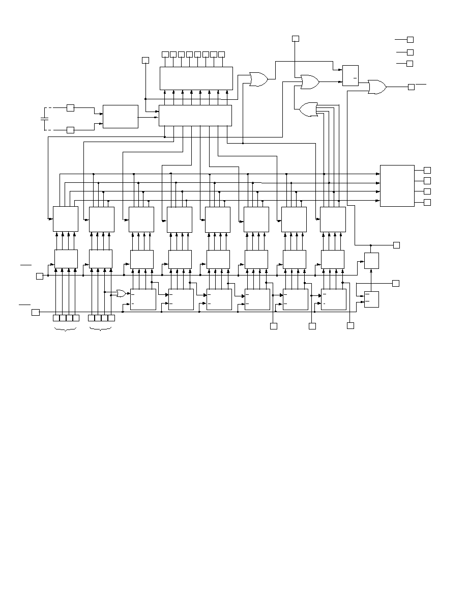
The LS7031 is a monolithic, ion implanted MOS, 6 decade up coun-
ter. The circuit includes latches, a multiplexer, leading zero blanking
and BCD data outputs.
CLOCK GENERATOR
The clock for the six decade counter (digit positions 3-8) is formed
from the internal `OR' combination of B4/D2 and B8/D2 if LS7031
is used with external prescaling counters. When operated in this
fashion the maximum allowable propagaton delay between B4/D2
(H-L) and B8/D2 (L-H), measured at Vss - 1V, is 10ns. If used as
a straight six decade counter, clock pulses may be applied to in-
puts B4/D2 or B8/D2 with the unused input held low. In either mode
of operation total pulse width must be minimum 62ns. See Block
Diagram.
6 DECADE UP COUNTER
The six decade ripple through counter increments on the negative
edge of the input count pulse. Maximum ripple time is 12µs
(999999 to 000000). Maximum count frequency is 7.5MHz.
RESET
All 6 counter decades are reset to zero when Reset input is brought
low for a minimum of 4µs. The Overflow flip-flop is reset at the
same time. Reset must be high for a minimum of 1µs before next
valid count can be recorded.
SCAN OSCILLATOR AND COUNTER
The scan counter is driven by an internal oscillator whose
frequency is determined by a capacitor connected between
Oscillator input and Scan input. An external scan clock applied
to Scan input can also drive the scan counter. Scan counter
advances on negative edge of scan clock.
The counter scans from MSD to LSD. When Scan Reset input is
brought high the scan counter is forced to MSD state. Internal
synchonization guarantees proper scanning no matter when Scan
Reset is brought low relative to scan clock. Maximum scan
frequency is 500kHz.
DECIMAL POINT
A high at the Decimal Point input resets the Blanking flip-flop
causing the display to unblank. Decimal Point should be brought
high at start of digit time which has active Decimal Point.
December 2002
7031-121102-1
LSI/CSI
LSI Computer Systems, Inc. 1235 Walt Whitman Road, Melville, NY 11747 (631) 271-0400 FAX (631) 271-0405
LS7031
LSI
1
2
3
4
5
6
7
8
9
10
11
12
13
14
15
16
17
18
19
20
21
22
23
24
25
26
27
28
29
30
31
32
33
34
35
36
37
38
39
40
FIGURE 1
CONNECTION DIAGRAM - TOP VIEW
OSC. INPUT
SCAN INPUT
N.C.
B 1 / D 1
B 2 / D 1
N.C.
B 4 / D 1
B 8 / D 1
N.C.
B 1 / D 2
B 2 / D 2
B 4 / D 2
V
SS
V
GG
N.C.
N.C.
V
DD
RESET COUNTER INPUT
LOAD LATCH INPUT
SCAN RESET INPUT
MSD STROBE 8
S T R O B E 7
S T R O B E 6
S T R O B E 5
S T R O B E 4
S T R O B E 3
S T R O B E 2
L S D S T R O B E 1
DECIMAL POINT INPUT
BLANK OUTPUT
O V E R F L O W O U T P U T
OVERFLOW INPUT
DECADE 8 OUTPUT, D8
DECADE 7 OUTPUT, D7
DECADE 6 OUTPUT, D6
B8
B4
B2
B1
BCD
DATA
O U T P U T S
DIGIT
S T R O B E
O U T P U T S
L S 7 0 3 1
INPUT TO
D E C A D E 1
LATCH
INPUT TO
D E C A D E 2
LATCH
B 8 / D 2
DIGIT STROBES
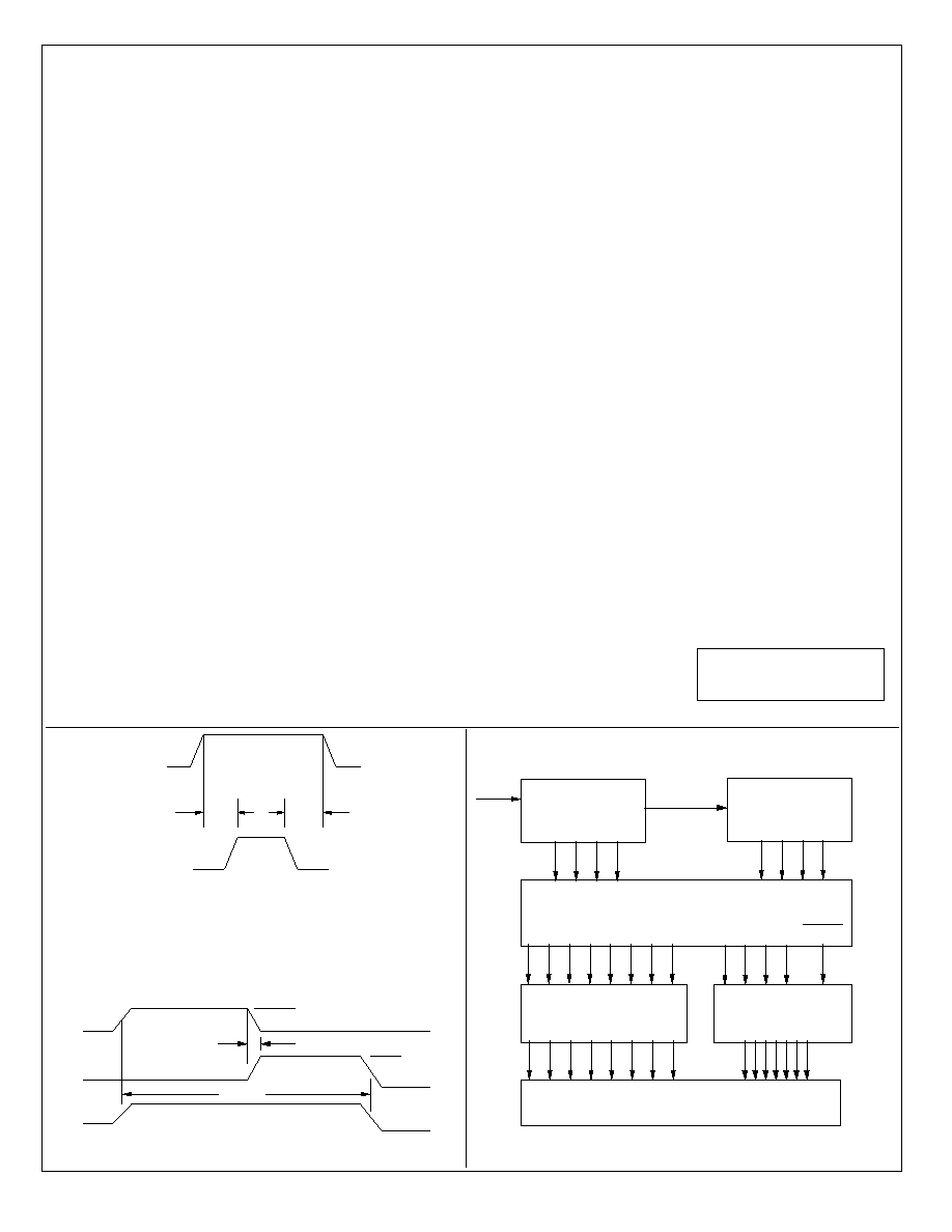
Timing of Digit Strobes is arranged such that both edges of strobe
are guardbanded by a minimum 400ns within valid BCD data when
scan frequency is 100kHz or less. The guardband is a minimum of
200ns at 250kHz scan frequency. At 500kHz only negative edge of
Strobe is guaranteed to be within valid BCD data by a minimum
200ns.
OVERFLOW
The Overflow flip-flop sets on the first negative transition of the Over-
flow Input and remains set until Reset is brought low. Data is trans-
ferred from Overflow flip-flop to Overflow Latch when Load is brought
low. A high at the Overflow Latch causes display to unblank. Over-
flow Output is output of Overflow Latch. MSB outputs of Decades
6, 7, 8 are available for use as Overflow Input.
LATCHES
Eight decades of latch are provided, two for storage of the two
external least significant decade counters and the remaining 6 for in-
ternal counter outputs. All latches when Load signal is brought low
for a minimum of 4µs and kept low until a minimum of 12µs has
elapsed from previous negative edge of count pulse (ripple time).
Storage of valid data occurs when Load signal is high for a minimum
of 1µs before next negative edge of count pulse or reset. Data is
transferred from Overflow flip-flop to Overflow latch at the same time.
UL
Æ
A3800

POWER SUPPLIES
+4.75V to +15V single power supply operation is obtained when
V
GG
and V
DD
are tied together. Inputs and outputs are CMOS
compatible and Minimum Input Noise Immunity of 25% of power
supply is guaranteed except for Decade 1 and 2 inputs.
(All inputs are TTL compatible at +4.75V to +5.25V operation.)
With V
GG
at -12V, V
DD
at OV and Vss at +5V all inputs are TTL
and CMOS compatible. All outputs are CMOS compatible and
BCD and BLANK outputs also provide standard TTL compat-
ibility. In addition, Overflow Output is low power TTL compatible.
In either mode outputs swing between V
DD
and Vss.
MAXIMUM RATINGS
PARAMETER
SYMBOL
VALUE
UNITS
Storage Temperature
Tstg
-65 to +150
∞C
Operating Temperature T
A
-25 to +70
∞C
Voltage (any pin to Vss) Vmax
-30 to +0.5
V
PARAMETER
SYMBOL
MIN
MAX
UNITS
Operating Supply Current
Idds
-
15
mA
(f
C
= 7.5MHz)
Input Noise Immunity
Low and High
Vni
25%
-
V
(Vss-V
DD
)
Input Voltage "0"
Vil
Vss - 20
Vss - 3.95
V
Input Voltage "1"
Vih
Vss - 1.0
Vss
V
Output Voltage "0"
Vol
-
+0.2
V
Output Voltage "1"
Voh
Vss - 1.0
-
V
Output Voltage "0"
(sinking 10µA)
Vol
-
+0.5
V
Output Current "1"
Vss = 4.75V(Voh = Vss - 0.5V)
-
0.05
-
mA
(Voh = Vss - 1V)
-
0.25
-
mA
(Voh = Vss - 4V)
-
0.90
-
mA
Vss = 10V (Voh = Vss - 2V)
-
2.0
-
mA
(Voh = Vss - 3V)
-
3.0
-
mA
Vss = 15V (Voh = Vss - 2V)
-
3.0
-
mA
(Voh = Vss - 3V)
-
4.5
-
mA
NOTE 1: Current Sink = Same as segment and strobe outputs.
Current Source = N/A at Voh = Vss - 0.5V for Vss = +4.75V
35µA at Voh = Vss -1V for Vss = +4.75V
40% of segment and strobe outputs at all other specified operating points.
NOTE 2: Limit segment current to 6mA maximum.
The following inputs have internal pull down resistors to V
DD
with maximum sink current of 5µA at Vss input.
Scan Reset B1/D1
B1/D2
Decimal B2/D1
B2/D2
Overflow B4/D1
B4/D2
B8/D1 B8/D2
DC ELECTRICAL CHARACTERISTICS
(V
DD
= V
GG
= OV, Vss = +4.75 to +15V, -25∞C
T
A
+70∞C unless otherwise specified.)
D6, D7, D8
OF, BCD
Blank
(See Note 1)
Segment
and
Strobe
Outputs
(See Note 2)
BLANKING
Leading zero blanking is employed. At start of each MSD to LSD
scan, display is blanked until a non-zero digit or active decimal
point is encountered. Display unblanks during LSD time and when-
ever Overflow output is high. When Scan Reset is applied, display
blanks to prevent display damage.
Blanking information is available at Blank output.
BCD DATA
Data is available in multiplexed BCD format. BCD data can be
readily demultiplexed using Digit Strobes as latch enable signals.
{
7031-110201-2
TTL COMPATIBLE OUTPUTS:
POWER SUPPLIES: Vss = +5V ± 5%, V
DD
= 0V, V
GG
= -12V ± 5%
OUTPUT LEVELS: "1" Level
Vss - 0.5V (sourcing 100µA)
"0" Level
0.4V (sinking 1.6mA)
"1" Level
Vss -.5V (sourcing 40µA)
"0" Level
0.4V (sinking .18mA)
All other outputs as specified for single power supply, Vss = +15V operation.
Inputs as specified for single power supply, Vss = +5V ± 5% operation.
}
}
BLANK AND BCD
DATA OUTPUTS
OVERFLOW
OUTPUT
{
EXTERNAL
DECADE
INPUTS
SCAN OSCILLATOR CAPACITANCE
TYPICAL OSCILLATOR FREQUENCY
4.75V 10V 15V
50pF
40.0 kHz
24.2kHz
22.2 kHz
100pF
22.2 kHz
14.8kHz
13.8 kHz
470pF
5.0 kHz
3.6kHz
3.5 kHz
ELECTRICAL CHARACtERISTICS:
(V
DD
= V
GG
= OV, Vss = +4.75 to +15V, -25∞C
T
A
+70∞C unless otherwise specified.)
PARAMETER
SYMBOL
MIN
MAX
UNITS
Count Test and Count frequency
(Vss = +5V ± 5%)
f
c
, f
tc
DC
7.5
MHz
(Vss = +10V)
f
c
, f
tc
DC
6
MHz
(Vss = +15V)
f
c
, f
tc
DC
5
MHz
Scan frequency
f
sc
DC
500
kHz
Count Pulse Width
(Pulse applied to B4/D2 or B8/D2;
`OR' combination ofB4/D2 and B8/D2)
(Vss = +5V ± 5%)
t
cpw
62
-
ns
(Vss = +10V)
t
cpw
83
-
ns
(Vss = +15V)
t
cpw
100
-
ns
**Propagation Delay
(B4/D2(H-L) to B8/D2 (L-H) at
Vss -1.0V)
Count Ripple Time
t
cr
Overlap
10
ns
Load Pulse Width
t
lpw
4
-
µs
Load Removal Time
t
lr
-
1
µs
Reset Pulse Width
t
rpw
4
-
µs
Reset Removal Time
t
rr
-
1
µs
Rise and Fall Time
Count Pulse
t
rfc
-
4
µs
Reset Pulse
t
rfr
-
4
µs
Test Count Pulse
t
rftc
-
80
µs
*Strobe Guard Band time
t
gb
400
-
ns
(fSC
100kHz
250kHz)
*Strobe Guard Band time
t
gb
200
-
ns
(100kHz
fSC
250kHz)
*Strobe Guard Band time
t
gb
200
-
ns
(250kHz
fSC
500kHz)
negative edge only
*Defines the minimum time from strobe edges to switching BCD data.
BCD CNTR 1
1 2 4 8
P R E S C A L E
DIGIT 1
B 1 / D 1 - B 8 / D 1
BCD CNTR 2
1 2 4 8
P R E S C A L E
DIGIT 2
B 1 / D 1 - B 8 / D 1
L S 7 0 3 1
DIGIT STROBES
1 2 4 8
BLANK
BCD TO SEVEN
S E G M E N T
D E C O D E R / D R I V E R
(LSD)
(MSD)
7 5 0 M H z
7 5 M H z
FIGURE 3. TYPICAL APPLICATION
DIGIT DRIVERS
8 DIGIT DISPLAY
7 . 5 M H z
b c d e f g
a
7031-110201-3
FIGURE 2. GUARD BANDED STROBE
BCD
t
gb
S T R O B E
t
gb
**Propagation Delay and Pulse Width
Vss - 1.0
Vss - 1.0
t
cpw
t
pr
B 4 / D 2
B 8 / D 2
B 4 / D 2
or
B 8 / D 2
The information included herein is believed to be
accurate and reliable. However, LSI Computer Systems,
Inc. assumes no responsibilities for inaccuracies, nor for
any infringements of patent rights of others which may
result from its use.
1
2
4 8
BCD
COUNTER
R
C
1
2
4
8
BCD
COUNTER
R
C
1
2 4
8
BCD
COUNTER
R
C
1 2
4
8
BCD
COUNTER
R
C
1
2
4
8
BCD
COUNTER
R
C
1 2
4 8
BCD
COUNTER
R
C
4 BIT
LATCH
ST
4 BIT
LATCH
ST
4 BIT
LATCH
ST
4 BIT
LATCH
ST
4 BIT
LATCH
ST
4 BIT
LATCH
ST
4 BIT
LATCH
ST
4 BIT
LATCH
ST
1 2 4 8
B1
B2
B4
B8
B1
B2
B4
B8
B1
B2
B4
B8
B1
B2
B4
B8
B1
B2
B4
MUX
GATE
G
B8
DATA
OUTPUT
BUFFER
D6 OUTPUT
D7 OUTPUT
D8 OUTPUT
OVFLW
F/F
OVERFLOW
INPUT
1 BIT
LATCH
BCD
DATA
OUTPUT
BLANK OUT
Vss
V
GG
V
DD
OVERFLOW
OUTPUT
ST
BLANKING
F/F
S
R
Q
C
R
NZ
8 DIGIT STROBE OUTPUTS
OUTPUT
BUFFERS
8 STATE STATIC SCAN
COUNTER & DECODED
LSD
MSD
R
C
OSCILLATOR
OR
BUFFER
SCAN RESET INPUT
(RESET TO MSD)
FIGURE 4. LS7031 BLOCK DIAGRAM
OSC. INPUT
SCAN INPUT
2
1
3
4
5
6
7
8
RESET
INPUT
LOAD
LATCH
INPUT
1 2 4 8
MUX
GATE
G
1 2 4 8
MUX
GATE
G
1 2 4 8
MUX
GATE
G
1 2 4 8
MUX
GATE
G
1 2 4 8
MUX
GATE
G
1 2 4 8
MUX
GATE
G
1 2 4 8
MUX
GATE
G
22
40
39
LSD
MSD
DECIMAL POINT
INPUT
10
27
26
23
11
12
13
14
15
16
21
9
8
7
6
5
4
3
2
1
B1 B2 B4 B8
B1 B2 B4 B8
DIGIT ONE
DIGIT TWO
31 30 29 28
37 36 34 33
B1
B2
B4
B8
20
19
18
17