 | –≠–ª–µ–∫—Ç—Ä–æ–Ω–Ω—ã–π –∫–æ–º–ø–æ–Ω–µ–Ω—Ç: MRF136 | –°–∫–∞—á–∞—Ç—å:  PDF PDF  ZIP ZIP |

The RF MOSFET Line
RF Power
Field-Effect Transistors
N-Channel Enhancement-Mode MOSFET
Designed for wideband large≠signal amplifier and oscillator applications up to
400 MHz range, in single ended configuration.
∑
Guaranteed 28 Volt, 150 MHz Performance
Output Power = 15 Watts
Narrowband Gain = 16 dB (Typ)
Efficiency = 60% (Typical)
∑
Small≠Signal and Large≠Signal
Characterization
∑
100% Tested For Load
Mismatch At All Phase
Angles With 30:1 VSWR
∑
Excellent Thermal Stability,
Ideally Suited For Class A
Operation
∑
Facilitates Manual Gain
Control, ALC and
Modulation Techniques
MAXIMUM RATINGS
Rating
Symbol
Value
Unit
Rating
Symbol
Value
Unit
Drain≠Source Voltage
VDSS
65
Vdc
Drain≠Gate Voltage (RGS = 1.0 M
)
VDGR
65
Vdc
Gate≠Source Voltage
VGS
±
40
Vdc
Drain Current -- Continuous
ID
2.5
Adc
Total Device Dissipation @ TC = 25
∞
C
Derate above 25
∞
C
PD
55
0.314
Watts
W/
∞
C
Storage Temperature Range
Tstg
≠ 65 to +150
∞
C
Operating Junction Temperature
TJ
200
∞
C
THERMAL CHARACTERISTICS
Characteristic
Symbol
Max
Unit
Characteristic
Symbol
Max
Unit
Thermal Resistance, Junction to Case
R
JC
3.2
∞
C/W
NOTE ≠ CAUTION ≠ MOS devices are susceptible to damage from electrostatic charge. Reasonable precautions in handling and
packaging MOS devices should be observed.
MRF136
15 W, to 400 MHz
N≠CHANNEL
MOS BROADBAND
RF POWER FET
CASE 211≠07, STYLE 2
D
G
S
Order this document
by MRF136/D
SEMICONDUCTOR TECHNICAL DATA
1
REV 7

ELECTRICAL CHARACTERISTICS
(TC = 25
∞
C unless otherwise noted.)
Characteristic
Symbol
Min
Typ
Max
Unit
OFF CHARACTERISTICS (1)
Drain≠Source Breakdown Voltage
(VGS = 0, ID = 5.0 mA)
V(BR)DSS
65
--
--
Vdc
Zero≠Gate Voltage Drain Current
(VDS = 28 V, VGS = 0)
IDSS
--
--
2.0
mAdc
Gate≠Source Leakage Current
(VGS = 40 V, VDS = 0)
IGSS
--
--
1.0
µ
Adc
ON CHARACTERISTICS (1)
Gate Threshold Voltage
(VDS = 10 V, ID = 25 mA)
VGS(th)
1.0
3.0
6.0
Vdc
Forward Transconductance
(VDS = 10 V, ID = 250 mA)
gfs
250
400
--
mmhos
DYNAMIC CHARACTERISTICS (1)
Input Capacitance
(VDS = 28 V, VGS = 0, f = 1.0 MHz)
Ciss
--
24
--
pF
Output Capacitance
(VDS = 28 V, VGS = 0, f = 1.0 MHz)
Coss
--
27
--
pF
Reverse Transfer Capacitance
(VDS = 28 V, VGS = 0, f = 1.0 MHz)
Crss
--
5.5
--
pF
FUNCTIONAL CHARACTERISTICS
Noise Figure
(VDS = 28 Vdc, ID = 500 mA, f = 150 MHz)
NF
--
1.0
--
dB
Common Source Power Gain (Figure 1)
(VDD = 28 Vdc, Pout = 15 W, f = 150 MHz, IDQ = 25 mA)
Gps
13
16
--
dB
Drain Efficiency (Figure 1)
(VDD = 28 Vdc, Pout = 15 W, f = 150 MHz, IDQ = 25 mA)
50
60
--
%
Electrical Ruggedness (Figure 1)
(VDD = 28 Vdc, Pout = 15 W, f = 150 MHz, IDQ = 25 mA,
VSWR 30:1 at all Phase Angles)
No Degradation in Output Power
NOTES:
1. Each side measured separately.
2
REV 7
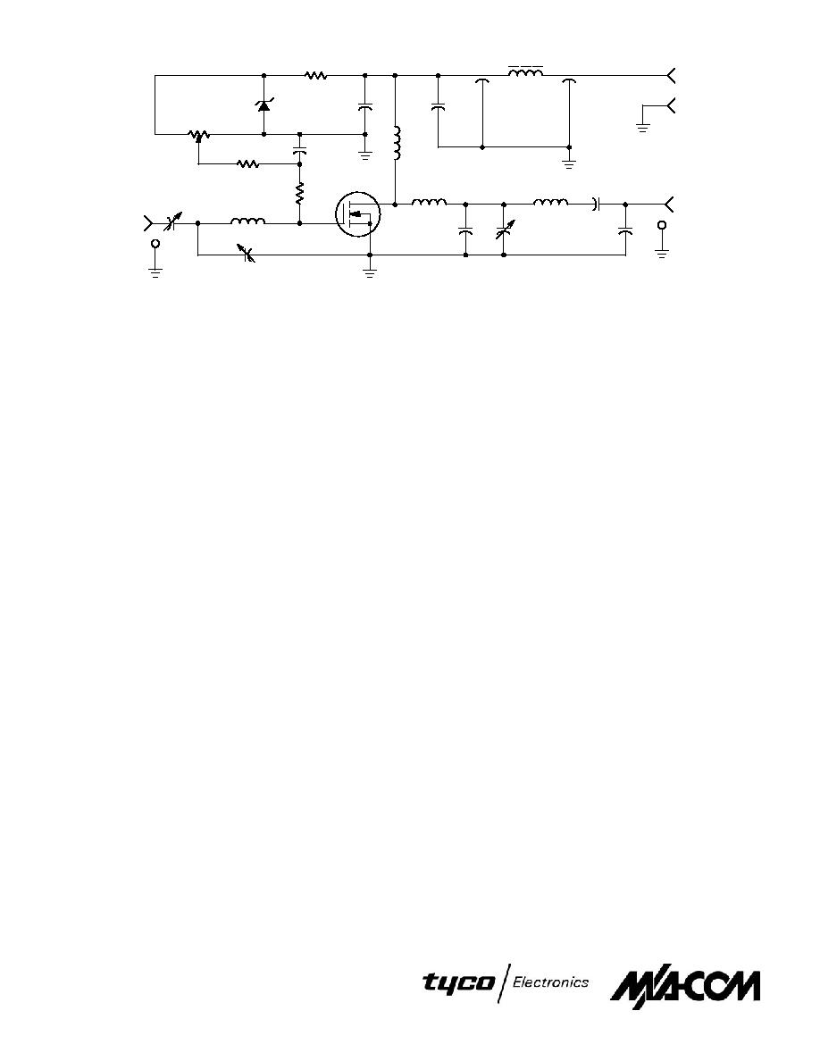
Figure 1. 150 MHz Test Circuit
C1, C2 -- Arco 406, 15 ≠ 115 pF or Equivalent
C3 -- Arco 404, 8 ≠ 60 pF or Equivalent
C4 -- 43 pF Mini≠Unelco or Equivalent
C5 -- 24 pF Mini≠Unelco or Equivalent
C6 -- 680 pF, 100 Mils Chip
C7 -- 0.01
µ
F Ceramic
C8 -- 100
µ
F, 40 V
C9 -- 0.1
µ
F Ceramic
C10, C11 -- 680 pF Feedthru
D1 -- 1N5925A Motorola Zener
L1 -- 2 Turns, 0.29
ID, #18 AWG, 0.10
Long
L2 -- 2 Turns, 0.23
ID, #18 AWG, 0.10
Long
L3 -- 2≠1/4 Turns, 0.29
ID, #18 AWG, 0.125
Long
RFC1 -- 20 Turns, 0.30
ID, #20 AWG Enamel Closewound
RFC2 -- Ferroxcube VK≠200 -- 19/4B
R1 -- 27
, 1 W Thin Film
R2 -- 10 k
, 1/4 W
R3 -- 10 Turns, 10 k
R4 -- 1.8 k
, 1/2 W
Board Material -- 0.062
G10, 1 oz. Cu Clad, Double Sided
R4
C10
D1
C8
+
RFC1
C7
C1
L1
R2
R1
C9
C4
C3
C2
RF INPUT
L2
RFC2
L3
DUT
≠
RF OUTPUT
C6
C5
C11
VDD = + 28 V
R3
BIAS
ADJUST
3
REV 7

TYPICAL CHARACTERISTICS
400
Figure 2. Output Power versus Input Power
Figure 3. Output Power versus Input Power
Figure 4. Output Power versus Input Power
Figure 5. Output Power versus Supply Voltage
Figure 6. Output Power versus Supply Voltage
Figure 7. Output Power versus Supply Voltage
20
20
18
16
14
12
10
8
6
4
2
0
0
200
600
800
1000
f = 100 MHz
f = 400 MHz
IDQ = 25 mA
150 MHz
200 MHz
f = 100 MHz
VDD = 13.5 V
IDQ = 25 mA
Pin, INPUT POWER (MILLWATTS)
P out
, OUTPUT
POWER (W
A
TTS)
20
18
16
14
12
10
8
6
4
2
0
0
1
2
3
4
Pin, INPUT POWER (WATTS)
P out
, OUTPUT
POWER (W
A
TTS)
10
9
8
7
6
5
4
3
2
1
0
0
200
400
600
800
1000
Pin, INPUT POWER (MILLWATTS)
P out
, OUTPUT
POWER (W
A
TTS)
200 MHz
150 MHz
24
21
18
15
12
9
6
3
0
12
16
20
24
28
VDD, SUPPLY VOLTAGE (VOLTS)
P out
, OUTPUT
POWER (W
A
TTS)
14
18
22
26
400 mW
200 mW
0.7 W
VDD = 28 V
VDD = 13.5 V
IDQ = 25 mA
f = 100 MHz
Pin = 600 mW
12
16
20
24
28
VDD, SUPPLY VOLTAGE (VOLTS)
P out
, OUTPUT
POWER (W
A
TTS)
14
18
22
26
600 mW
300 mW
IDQ = 25 mA
f = 150 MHz
Pin = 900 mW
24
21
18
15
12
9
6
3
0
12
16
20
24
28
VDD, SUPPLY VOLTAGE (VOLTS)
P out
, OUTPUT
POWER (W
A
TTS)
14
18
22
26
0.4 W
Pin = 1 W
IDQ = 25 mA
f = 200 MHz
VDD = 28 V
IDQ = 25 mA
24
21
18
15
12
9
6
3
0
4
REV 7
TYPICAL CHARACTERISTICS
VGS, GATE≠SOURCE VOLTAGE (VOLTS)
Figure 8. Output Power versus Supply Voltage
Figure 9. Output Power versus Gate Voltage
Figure 10. Drain Current versus Gate Voltage
(Transfer Characteristics)
Figure 11. Gate≠Source Voltage versus
Case Temperature
Figure 12. Capacitance versus Drain≠Source Voltage
Figure 13. DC Safe Operating Area
12
16
20
24
28
VDD, SUPPLY VOLTAGE (VOLTS)
P out
, OUTPUT
POWER (W
A
TTS)
14
18
22
26
2 W
IDQ = 25 mA
f = 400 MHz
Pin = 3 W
2
1.8
1.6
1.4
1.2
1
0.8
0.6
0.4
0.2
0
20
18
16
14
12
10
8
6
4
2
0
0
16
20
24
28
VDS, DRAIN≠SOURCE VOLTAGE (VOLTS)
≠ 25
25
75
125
175
TC, CASE TEMPERATURE (
∞
C)
0
50
100
150
0.94
≠ 7
P out
, OUTPUT
POWER (W
A
TTS)
16
14
12
10
8
6
4
2
0
4
8
12
1.04
1.03
1.02
1.01
1
0.99
0.98
0.97
0.96
0.95
0
4
5
6
7
VDS, GATE≠SOURCE VOLTAGE (VOLTS)
1
2
3
0
100
180
60
40
20
≠ 6
≠ 5
≠ 4
≠ 3
≠ 2
≠1
0
1
2
3
1 W
VDS = 28 V
ID = 750 mA
25 mA
500 mA
250 mA
1
30
20
50
100
VDS, DRAIN≠SOURCE VOLTAGE (VOLTS)
2
3
5
0.1
10
70
10
5
3
2
1
0.3
0.2
VDS = 10 V
TYPICAL DEVICE
SHOWN, VGS(th) = 3 V
VDD = 28 V
IDQ = 25 mA
Pin = CONSTANT
TYPICAL DEVICE
SHOWN, VGS(th) = 3 V
VGS = 0 V
f = 1 MHz
Coss
Ciss
Crss
TC = 25
∞
C
400 MHz
400 MHz
150 MHz
I D
, DRAIN CURRENT
(MILLAMPS)
I D
, DRAIN CURRENT
(AMPS)
C, CAP
ACIT
ANCE
(pF)
V
GS
, GA
TE-SOURCE
VOL
T
AGE
(NORMALIZED)
5
REV 7

TYPICAL CHARACTERISTICS
Figure 14. Output Power versus Input Power
Figure 15. Output Power versus Gate Voltage
TYPICAL 400 MHz PERFORMANCE
VDD = 28 V
IDQ = 100 mA
f = 400 MHz
VDD = 28 V
IDQ = 100 mA
Pin = CONSTANT
TYPICAL DEVICE
SHOWN, VGS(th) = 3 V
40
35
30
25
20
15
10
5
0
≠ 4
≠ 2
0
2
4
VGS, GATE≠SOURCE VOLTAGE (VOLTS)
P out
, OUTPUT
POWER (W
A
TTS)
≠ 3
≠1
1
3
40
35
30
25
20
15
10
5
0
0
1
2.5
3.5
Pin, INPUT POWER (WATTS)
P out
, OUTPUT
POWER (W
A
TTS)
0.5
1.5
2
3
f = 400 MHz
6
REV 7

Figure 16. Large≠Signal Series Equivalent
Input Impedance, Zin
Figure 17. Large≠Signal Series Equivalent
Output Impedance, ZOL*
Figure 18. Input and Outut Impedance
400
200
150
f = 100 MHz
Zin
{
VDD = 28 V, IDQ = 25 mA,
Pout = 15 W
{
27
Shunt Resistor Gate≠to≠Ground
f
MHz
Zin
{
OHMS
100
150
200
400
7.5 ≠ j9.73
4.11 ≠ j7.56
2.66 ≠ j6.39
2.39 ≠ j2.18
400
200
150
f = 100 MHz
ZOL*
VDD = 28 V, IDQ = 25 mA,
Pout = 15 W
ZOL* = Conjugate of the
optimum load impedance into
which the device operates at
a given output power, voltage
and frequency.
f
MHz
ZOL*
OHMS
100
150
200
400
13.7 ≠ j16.8
9.08 ≠ j15.38
4.74 ≠ j8.92
4.28 ≠ j4.17
400
225
150
f = 30 MHz
ZOL*
100
50
Zin
f = 30 MHz
50
100
150
225
400
Feedback loops: 560 ohms in series with 0.1
µ
F
Drain to gate, each side of push≠pull FET
ZOL* = Conjugate of the optimum load imped-
ance into which the device operates at a given
output power, voltage and frequency.
VDD = 28 V, IDQ = 100 mA,
Pout = 30 W
f
MHz
Zin
{
Ohms
ZOL*
Ohms
30
50
100
150
225
400
59.3 ≠ j24
48 ≠ j33.5
20.5 ≠ j34.2
4.77 ≠ j25.4
3
≠ j9.5
2.34 ≠ j3.31
40.1 ≠ j8.52
37 ≠ j11.9
29 ≠ j16.5
20.6 ≠ j19
13 ≠ j16.7
10.2 ≠ j14.3
Zin & ZOL* are given
from drain≠to≠drain and
gate≠to≠gate respectively.
7
REV 7

f
S11
S21
S12
S22
f
(MHz)
|S11|
|S21|
|S12|
|S22|
2.0
0.988
≠ 11
41.19
173
0.006
67
0.729
≠ 12
5.0
0.970
≠ 27
40.07
164
0.014
62
0.720
≠ 31
10
0.923
≠ 52
35.94
149
0.026
54
0.714
≠ 58
20
0.837
≠ 88
27.23
129
0.040
36
0.690
≠ 96
30
0.784
≠ 111
20.75
117
0.046
27
0.684
≠ 118
40
0.751
≠ 125
16.49
108
0.048
22
0.680
≠ 131
50
0.733
≠ 135
13.41
103
0.050
19
0.679
≠ 139
60
0.720
≠ 1 42
11.43
99
0.050
16
0.678
≠ 145
70
0.709
≠ 147
9.871
96
0.050
14
0.679
≠ 149
80
0.707
≠ 152
8.663
93
0.051
13
0.683
≠ 153
90
0.706
≠ 155
7.784
91
0.051
13
0.682
≠ 155
100
0.708
≠ 157
7.008
88
0.051
13
0.680
≠ 157
110
0.711
≠ 159
6.435
86
0.051
14
0.681
≠ 158
120
0.714
≠ 161
5.899
85
0.051
15
0.682
≠ 159
130
0.717
≠ 163
5.439
82
0.052
16
0.684
≠ 160
140
0.720
≠ 164
5.068
80
0.052
17
0.684
≠ 161
150
0.723
≠ 165
4.709
80
0.052
18
0.686
≠ 161
160
0.727
≠ 166
4.455
78
0.052
18
0.690
≠ 161
170
0.732
≠ 167
4.200
77
0.052
18
0.694
≠ 162
180
0.735
≠ 168
3.967
75
0.052
19
0.699
≠ 162
190
0.738
≠ 169
3.756
74
0.052
19
0.703
≠ 163
200
0.740
≠ 170
3.545
73
0.052
20
0.706
≠ 163
225
0.746
≠ 171
3.140
69
0.053
22
0.717
≠ 163
250
0.742
≠ 172
2.783
67
0.053
25
0.724
≠ 163
275
0.744
≠ 173
2.540
64
0.054
27
0.724
≠ 163
300
0.751
≠ 174
2.323
60
0.055
29
0.736
≠ 163
325
0.757
≠ 175
2.140
58
0.058
32
0.749
≠ 163
350
0.760
≠ 176
1.963
54
0.059
35
0.758
≠ 163
375
0.762
≠ 177
1.838
52
0.062
38
0.768
≠ 163
400
0.774
≠ 179
1.696
50
0.065
41
0.783
≠ 163
425
0.775
≠ 179
1.590
48
0.068
43
0.793
≠ 163
450
0.781
+ 179
1.493
46
0.071
46
0.805
≠ 163
475
0.787
+ 177
1.415
43
0.074
47
0.813
≠ 164
500
0.792
+ 176
1.332
40
0.079
48
0.825
≠ 164
525
0.797
+ 175
1.259
38
0.083
50
0.831
≠ 164
550
0.801
+ 175
1.185
37
0.088
51
0.843
≠ 164
575
0.810
+ 174
1.145
36
0.094
52
0.855
≠ 164
600
0.816
+ 173
1.091
34
0.101
52
0.869
≠ 165
625
0.818
+ 171
1.041
32
0.106
53
0.871
≠ 165
650
0.825
+ 170
0.994
30
0.112
53
0.884
≠ 165
675
0.834
+ 169
0.962
29
0.119
53
0.890
≠ 165
700
0.837
+ 168
0.922
27
0.127
53
0.906
≠ 166
725
0.836
+ 167
0.879
25
0.133
52
0.909
≠ 167
750
0.841
+ 166
0.838
25
0.140
53
0.917
≠ 167
775
0.844
+ 165
0.824
24
0.148
52
0.933
≠ 167
800
0.846
+ 163
0.785
21
0.154
50
0.941
≠ 168
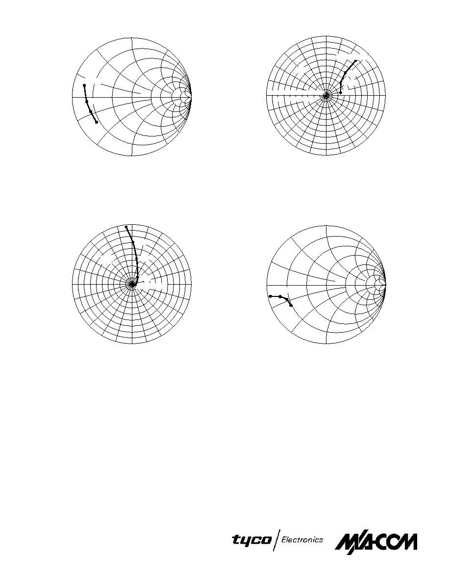
Table 1. Common Source Scattering Parameters
VDS = 28 V, ID = 0.5 A
8
REV 7
S11
+90
∞
+120
∞
+150
∞
0
∞
≠150
∞
≠120
∞
≠ 60
∞
≠ 30
∞
+30
∞
+60
∞
S12
70
10
25
50
100 150 250
500
+j50
+j100
+j150
+j250
+j500
≠ j500
≠ j250
≠ j150
≠ j100
≠ j50
≠ j25
≠ j10
0
+j10
+j25
400
70
S22
150
Figure 19. S11, Input Reflection Coefficient
versus Frequency
VDS = 28 V ID = 0.5 A
Figure 20. S12, Reverse Transmission Coefficient
versus Frequency
VDS = 28 V ID = 0.5 A
Figure 21. S21, Forward Transmission Coefficient
versus Frequency
VDS = 28 V ID = 0.5 A
Figure 22. S22, Output Reflection Coefficient
versus Frequency
VDS = 28 V ID = 0.5 A
10
25
50
100 150
250
500
+j50
+j100
+j150
+j250
+j500
≠ j500
≠ j250
≠ j150
≠ j100
≠ j50
≠ j25
≠ j10
0
+j10
+j25
+90
∞
+120
∞
+150
∞
180
∞
0
∞
≠150
∞
≠120
∞
≠ 90
∞
≠ 60
∞
≠ 30
∞
+30
∞
+60
∞
f = 800 MHz
8
4
2
6
400
100
150
70
≠90
∞
0.16
0.12
0.08
0.04
0.06
600
0.02
0.18
180
∞
0.14
0.10
400
f = 800 MHz
400
150
70
S21
f = 800 MHz
f = 800 MHz
9
REV 7

DESIGN CONSIDERATIONS
The MRF136 is an RF power N≠Channel enhancement
mode field≠effect transistor (FET) designed especially for HF
and VHF power amplifier applications. M/A-COM RF MOS
FETs feature planar design for optimum manufacturability.
M/A-COM Application Note AN211A, FETs in Theory and
Practice, is suggested reading for those not familiar with the
construction and characteristics of FETs.
The major advantages of RF power FETs include high gain,
low noise, simple bias systems, relative immunity from ther-
mal runaway, and the ability to withstand severely mis-
matched loads without suffering damage. Power output can
be varied over a wide range with a low power dc control signal,
thus facilitating manual gain control, ALC and modulation.
DC BIAS
The MRF136 is an enhancement mode FET and, therefore,
does not conduct when drain voltage is applied without gate
bias. A positive gate voltage causes drain current to flow (see
Figure 10). RF power FETs require forward bias for optimum
gain and power output. A Class AB condition with quiescent
drain current (IDQ) in the 25≠100 mA range is sufficient for
many applications. For special requirements such as linear
amplification, IDQ may have to be adjusted to optimize the
critical parameters.
The MOS gate is a dc open circuit. Since the gate bias circuit
does not have to deliver any current to the FET, a simple
resistive divider arrangement may sometimes suffice for this
function. Special applications may require more elaborate
gate bias systems.
GAIN CONTROL
Power output of the MRF136 may be controlled from rated
values down to the milliwatt region (>20 dB reduction in power
output with constant input power) by varying the dc gate
voltage. This feature, not available in bipolar RF power
devices, facilitates the incorporation of manual gain control,
AGC/ALC and modulation schemes into system designs. A
full range of power output control may require dc gate voltage
excursions into the negative region.
AMPLIFIER DESIGN
Impedance matching networks similar to those used with
bipolar transistors are suitable for MRF136. See M/A-COM
Application Note AN721, Impedance Matching Networks
Applied to RF Power Transistors. Both small signal scattering
parameters and large signal impedance parameters are
provided. Large signal impedances should be used for
network designs wherever possible. While the s parameters
will not produce an exact design solution for high power
operation, they do yield a good first approximation. This is
particularly useful at frequencies outside those presented in
the large signal impedance plots.
RF power FETs are triode devices and are therefore not
unilateral. This, coupled with the very high gain, yields a
device capable of self oscillation. Stability may be achieved
using techniques such as drain loading, input shunt resistive
loading, or feedback. S parameter stability analysis can
provide useful information in the selection of loading and/or
feedback to insure stable operation. The MRF136 was
characterized with a 27 ohm input shunt loading resistor.
For further discussion of RF amplifier stability and the use
of two port parameters in RF amplifier design, see M/A-COM
Application Note AN215A.
LOW NOISE OPERATION
Input resistive loading will degrade noise performance, and
noise figure may vary significantly with gate driving imped-
ance. A low loss input matching network with its gate
impedance optimized for lowest noise is recommended.
10
REV 7

PACKAGE DIMENSIONS
CASE 211≠07
ISSUE N
NOTES:
1. DIMENSIONING AND TOLERANCING PER ANSI
Y14.5M, 1982.
2. CONTROLLING DIMENSION: INCH.
A
U
M
M
Q
R
B
1
4
3
2
D
K
E
SEATING
PLANE
C
J
H
S
DIM
MIN
MAX
MIN
MAX
MILLIMETERS
INCHES
A
0.960
0.990
24.39
25.14
B
0.370
0.390
9.40
9.90
C
0.229
0.281
5.82
7.13
D
0.215
0.235
5.47
5.96
E
0.085
0.105
2.16
2.66
H
0.150
0.108
3.81
4.57
J
0.004
0.006
0.11
0.15
K
0.395
0.405
10.04
10.28
M
40
50
40
50
Q
0.113
0.130
2.88
3.30
R
0.245
0.255
6.23
6.47
S
0.790
0.810
20.07
20.57
U
0.720
0.730
18.29
18.54
_
_
_
_
STYLE 2:
PIN 1. SOURCE
2. GATE
3. SOURCE
4. DRAIN
11
Specifications subject to change without notice.
n
North America: Tel. (800) 366-2266, Fax (800) 618-8883
n
Asia/Pacific: Tel.+81-44-844-8296, Fax +81-44-844-8298
n
Europe: Tel. +44 (1344) 869 595, Fax+44 (1344) 300 020
Visit www.macom.com for additional data sheets and product information.
REV 7