 | –≠–ª–µ–∫—Ç—Ä–æ–Ω–Ω—ã–π –∫–æ–º–ø–æ–Ω–µ–Ω—Ç: MRF321 | –°–∫–∞—á–∞—Ç—å:  PDF PDF  ZIP ZIP |

The RF Line
NPN Silicon
RF Power Transistor
. . . designed primarily for wideband large≠signal driver and predriver amplifier
stages in 200≠500 MHz frequency range.
∑
Guaranteed Performance at 400 MHz, 28 Vdc
Output Power = 10 Watts
Power Gain = 12 dB Min
Efficiency = 50% Min
∑
100% Tested for Load Mismatch at all Phase Angles with 30:1 VSWR
∑
Gold Metallization System for High Reliability
∑
Computer≠Controlled Wirebonding Gives Consistent Input Impedance
MAXIMUM RATINGS
Rating
Symbol
Value
Unit
Collector≠Emitter Voltage
V
CEO
33
Vdc
Collector≠Base Voltage
V
CBO
60
Vdc
Emitter≠Base Voltage
V
EBO
4.0
Vdc
Collector Current -- Continuous
Collector Current
-- Peak
I
C
1.1
1.5
Adc
Total Device Dissipation @ T
A
= 25
∞
C (1)
Derate above 25
∞
C
P
D
27
160
Watts
mW/
∞
C
Storage Temperature Range
T
stg
≠65 to +150
∞
C
THERMAL CHARACTERISTICS
Characteristic
Symbol
Max
Unit
Thermal Resistance, Junction to Case
R
JC
6.4
∞
C/W
ELECTRICAL CHARACTERISTICS
(T
C
= 25
∞
C unless otherwise noted.)
Characteristic
Symbol
Min
Typ
Max
Unit
OFF CHARACTERISTICS
Collector≠Emitter Breakdown Voltage
(I
C
= 20 mAdc, I
B
= 0)
V
(BR)CEO
33
--
--
Vdc
Collector≠Emitter Breakdown Voltage
(I
C
= 20 mAdc, V
BE
= 0)
V
(BR)CES
60
--
--
Vdc
Collector≠Base Breakdown Voltage
(I
C
= 20 mAdc, I
E
= 0)
V
(BR)CBO
60
--
--
Vdc
Emitter≠Base Breakdown Voltage
(I
E
= 2.0 mAdc, I
C
= 0)
V
(BR)EBO
4.0
--
--
Vdc
Collector Cutoff Current
(V
CB
= 30 Vdc, I
E
= 0)
I
CBO
--
--
1.0
mAdc
ON CHARACTERISTICS
DC Current Gain
(I
C
= 500 mA, V
CE
= 5.0 Vdc)
h
FE
20
--
80
--
NOTE:
(continued)
1. This device is designed for RF operation. The total device dissipation rating applies only when the device is operated as an RF amplifier.
MRF321
10 W, 400 MHz
RF POWER
TRANSISTOR
NPN SILICON
CASE 244≠04, STYLE 1
Order this document
by MRF321/D
SEMICONDUCTOR TECHNICAL DATA
1
ELECTRICAL CHARACTERISTICS -- continued
(T
C
= 25
∞
C unless otherwise noted.)
Characteristic
Unit
Max
Typ
Min
Symbol
DYNAMIC CHARACTERISTICS
Output Capacitance
(V
CB
= 28 Vdc, I
E
= 0, f = 1.0 MHz)
C
ob
--
10
12
pF
FUNCTIONAL TESTS (Figure 1)
Common≠Emitter Amplifier Power Gain
(V
CC
= 28 Vdc, P
out
= 10 W, f = 400 MHz)
G
PE
12
13
--
dB
Collector Efficiency
(V
CC
= 28 Vdc, P
out
= 10 W, f = 400 MHz)
50
60
--
%
Load Mismatch
(V
CC
= 28 Vdc, P
out
= 10 W, f = 400 MHz,
VSWR = 30:1 all phase angles)
No Degradation in Output Power
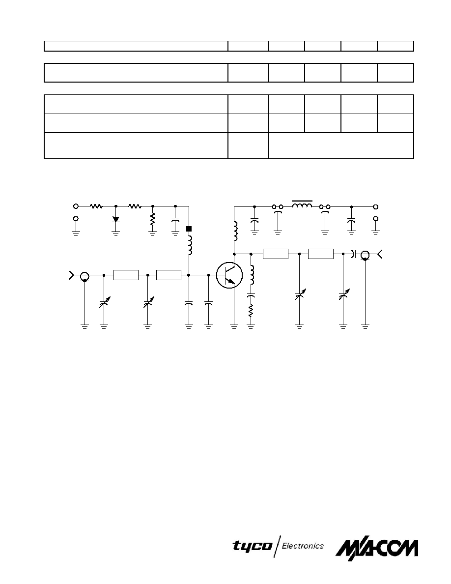
Figure 1. 400 MHz Test Circuit Schematic
C1, C2, C3 -- 1.0≠20 pF Johanson Trimmer (JMC 5501)
C3, C4 -- 47 pF ATC Chip Capacitor
C5, C10 -- 0.1
µ
F Erie Redcap
C7 -- 0.5≠10 pF Johanson Trimmer (JMC 5201)
C8 -- 0.018
µ
F Vitramon Chip Capacitor
C9 -- 200 pF UNELCO Capacitor
C11, C12 -- 680 pF Feedthru
C13 -- 1.0
µ
F, 50 Volt Tantalum Capacitor
D1 -- 1N4001
L1 -- 0.33
µ
H Molded Choke with Ferroxcube Bead
L1 --
(Ferroxcube 56≠590≠65/4B) on Ground End of Coil
L2 -- 4 Turns #20 Enamel, 1/8
ID
L3 -- 6 Turns #20 Enamel, 1/4
ID
L4 -- Ferroxcube VK200≠19/4B
R1 -- 5.1
, 1/4 Watt
R2 -- 120
, 1.0 Watt
R3 -- 20
, 1/2 Watt
R4 -- 47
, 1/2 Watt
Z1 -- Microstrip 0.1
W x 1.35
L
Z2 -- Microstrip 0.1
W x 0.55
L
Z3 -- Microstrip 0.1
W x 0.8
L
Z4 -- Microstrip 0.1
W x 1.75
L
Board -- Glass Teflon,
R
= 2.56, t = 0.062
Input/Output Connectors -- Type N
R2
R3
D1
R4
C9
L1
L3
C10
C11
L4
C12
C13
+
-
+
-
28 V
RF
OUTPUT
RF
INPUT
Z1
Z2
Z3
Z4
C8
C1
C2
C3
C4
C5
R1
C6
C7
DUT
L2
+
-
5 V
2

Figure 2. Output Power versus Frequency
Figure 3. Output Power versus Input Power
Figure 4. Output Power versus Supply Voltage
Figure 5. Power Gain versus Frequency
P
, OUTPUT
POWER (W
A
TTS)
out
12
f, FREQUENCY (MHz)
600
10
8
6
4
2
500
400
300
200
100
P
, OUTPUT
POWER (W
A
TTS)
out
12
P
in
, INPUT POWER (mW)
10
8
6
4
2
300
0
600
900
1200
1500
P
, OUTPUT
POWER (W
A
TTS)
out
12
V
CC
, SUPPLY VOLTAGE (VOLTS)
10
8
6
4
2
14
10
18
22
26
30
22
f, FREQUENCY (MHz)
18
500
400
300
200
14
10
6
2
G
PE
, COMMON EMITTER
AMPLIFIER
POWER GAIN (dB)
V
CC
= 28 V
P
in
= 0.5 W
0.35 W
f = 400 MHz
P
o
= 10 W
V
CC
= 28 V
0.7 W
0.5 W
0.4 W
0.3 W
0.2 W
P
in
= 1 W
0.1 W
V
CC
= 28 V
400
500
f = 200 MHz
3

Figure 6. Series Equivalent Impedance
Z
in
0
10
-10
Z
OL
* = Conjugate of the optimum load impedance into which the device output operates at a given output power,
Z
OL
* =
voltage and frequency.
5
-5
f = 200 MHz
400
Z
OL
*
5
15
20
25
500
f = 200 MHz
400
500
P
o
= 10 W, V
CC
= 28 V
f
MHz
Z
in
Ohms
Z
OL
*
Ohms
200
400
500
0.68 - j0.75
0.89 + j2.7
1.3 + j4.3
14.2 - j22
9.8 - j14.4
9.3 - j13
4

PACKAGE DIMENSIONS
CASE 244≠04
ISSUE J
STYLE 1:
PIN 1. EMITTER
2. BASE
3. EMITTER
4. COLLECTOR
K
D
A
J
T
F
P
M
2
1
3
4
SEATING PLANE
8-32 NC 2A
WRENCH FLAT
U
E
B
S
C
DIM
MIN
MAX
MIN
MAX
INCHES
MILLIMETERS
A
7.06
7.26
0.278
0.286
B
6.20
6.50
0.244
0.256
C
14.99
16.51
0.590
0.650
D
5.46
5.96
0.215
0.235
E
1.40
1.65
0.055
0.065
G
1.52
---
0.060
---
J
0.08
0.17
0.003
0.007
K
11.05
---
0.435
---
M
45 NOM
45 NOM
P
---
1.27
---
0.050
S
3.00
3.25
0.118
0.128
T
1.40
1.77
0.055
0.070
U
2.92
3.68
0.115
0.145
_
_
5
Specifications subject to change without notice.
n
North America: Tel. (800) 366-2266, Fax (800) 618-8883
n
Asia/Pacific: Tel.+81-44-844-8296, Fax +81-44-844-8298
n
Europe: Tel. +44 (1344) 869 595, Fax+44 (1344) 300 020
Visit www.macom.com for additional data sheets and product information.