3 Volt, 2 Watt Cellular T/R Changeover Switch, DC - 2.0 GHz
SW-392
M/A-COM Division of AMP Incorporated
3
North America: Tel. (800) 366-2266, Fax (800) 618-8883
3
Asia/Pacific: Tel.+85 2 2111 8088, Fax +85 2 2111 8087
3
Europe: Tel. +44 (1344) 869 595, Fax+44 (1344) 300 020
www.macom.com
AMP and Connecting at a Higher Level are trademarks.
Specifications subject to change without notice.
V2.00
Features
∑
Low Cost Plastic SOT-26 Package
∑
Low Insertion Loss < 0.6 dB @ 900 MHz
∑
Low Power Consumption < 20
µ
A @ +3V
∑
Very High Intercept Point: 52 dBm IP
3
∑
Both Positive and Negative 3 to 8 V Control
∑
For AMPS, NAMPS, ETACS, NMT, GSM, PCN, PDC and
DECT Applications
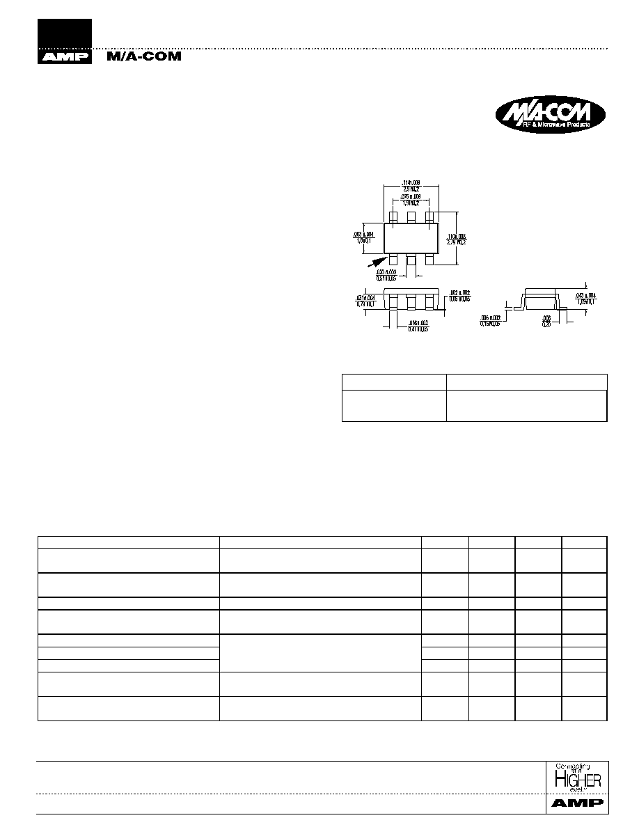
SOT-26
1
Electrical Specifications: T
A
= +25∞C
1
3 Volt, 2 Watt Cellular T/R Changeover Switch
DC - 2.0 GHz
SW-392
Parameter
Test Conditions
Units
Min.
Typ.
Max.
Insertion Loss
DC - 1.0 GHz
dB
0.55
0.65
1.0 - 2.0 GHz
dB
0.8
1.0
Isolation
DC - 1.0 GHz
dB
15
17
1.0 - 2.0 GHz
dB
8
10
VSWR
DC - 2.0 GHz
1.3:1
1 dB Compression
Input Power (3V Control) 0.9 GHz
dBm
35
Input Power (5V Control) 0.9 GHz
dBm
37
T
rise
, T
fall
10% to 90% RF, 90% to 10% RF
µ
S
15
T
on
, T
off
50% Control to 90% RF, Control to 10% RF
µ
S
20
Transients
In-band
mV
60
Input IP
2
2-Tone, 5 MHz spacing, 0.9 GHz
dBm
95
+10 dBm (+13 dBm total)
Input IP
3
2-Tone, 5 MHz spacing, 0.9 GHz
dBm
52
+10 dBm (+13 dBm total)
Description
M/A-COM's SW-392 is a GaAs Monolithic switch in a low cost
SOT-26 surface mount plastic package. The SW-392 is ideally
suited for applications where very low power consumption
(<20µA @ 3V), low intermodulation products, very small size
and low cost required. Typical application is an Internal/Exter-
nal antenna select switch for portable telephones and data radios.
In addition, because of its low loss, good isolation, and inherent
speed, the SW-392 can be used in power applications up to 2
Watts in systems such as cellular, PCN, GSM and other analog/
digital wireless communications systems.
The SW-392 is fabricated using a mature 1-micron gate length
GaAs MESFET process. The process features full chip passiva-
tion for increased performance and reliability.
Ordering Information
Part Number
Package
SW-392 PIN
SOT-26 Plastic Package
SW-392TR
Forward Tape and Reel
1
1. Refer to Application Note M513 for reel size information.
1.
All measurements at 1 GHz in a 50
system unless otherwise specified. Loss varies at 0.003 dB/∞C.
PIN 1
XX#Y
1. Dimensions are in: inches/mm

3 Volt, 2 Watt Cellular T/R Changeover Switch, DC - 2.0 GHz
SW-392
M/A-COM Division of AMP Incorporated
3
North America: Tel. (800) 366-2266, Fax (800) 618-8883
3
Asia/Pacific: Tel.+85 2 2111 8088, Fax +85 2 2111 8087
3
Europe: Tel. +44 (1344) 869 595, Fax+44 (1344) 300 020
www.macom.com
AMP and Connecting at a Higher Level are trademarks.
Specifications subject to change without notice.
V2.00
0
5
10
15
20
25
30
35
40
-3
-4
-5
-6
-7
-8
CONTROL VOLTAGE (VOLTS)
COMPRESSION (dBm)
&2035(66,2132,17YV&21752/92/7$*(#0+]
0.1dB
1dB
ISOLATION vs FREQUENCY
-50
-40
-30
-20
-10
0
0
0.5
1
1.5
2
2.5
FREQUENCY (GHz)
ISOLATION (dB)
VSWR vs FREQUENCY
1
1.2
1.4
1.6
1.8
2
0
0.5
1
1.5
2
2.5
3
FREQUENCY (GHz)
VSWR
INPUT
OUTPUT
INSERTION LOSS vs FREQUENCY
-2
-1.5
-1
-0.5
0
0
0.5
1
1.5
2
2.5
FREQUENCY (GHz)
INSERTION LOSS (dB)
Parameter
Absolute Maximum
Max. Input Power (0.5 - 2.5 GHz)
3V Control
+34 dBm
5V Control
+37 dBm
Operating Temperature
-40∞C to +85∞C
Storage Temperature
-65∞C to +150∞C
Thermal Temperature
jc = +87∞C/W
Absolute Maximum Ratings
1
1.
Exceeding any one or a combination of these limits may cause
permanent damage.
2.
Thermal resistance is given for T
A
= +25∞C.
Typical Performance Curves
Insertion Loss vs. Frequency
VSWR vs. Frequency
Isolation vs Frequency
Functional Schematic
Mode (Control) Control A
Control B
RFC - RF1
RFC - RF2
Postive
1
0±0.2V
+3 to +8V
+3V to +8V
0±0.2V
Off
On
On
Off
Postive/
Negative
1,2
-Vc±0.2V
+Vc
+Vc
-Vc±0.2V
On
Off
Off
On
Negative
3
0±0.2V
-3V to -8V
-3V to -8V
0±0.2V
On
Off
Off
On
Truth Table
1. External DC blocking capacitors are required on all RF ports.
2. |-Vc|+ Vc <
8 V.
3. If negative control is used, DC blocking capacitors are not re-
quired on RF ports.
Two Tone IP
3
Measurements
Control
Voltage
(VDC)
Input
Power
(dBm)
3rd Order
Intermodulation
Products (dBc)
IP
3
(dBm)
Second
Harmonic
(dBc)
0,3
27
33
43
64
0,5
27
66
60
61
0,8
27
66
60
59
0,3
28
31
43
61
0,5
28
61
58
59
0,8
28
66
61
60
0,3
29
31
44
59
0,5
29
55
57
58
0,8
29
66
62
61
0,3
30
30
45
53
0,5
30
47
54
59
0,8
30
65
63
58
Compression Point vs Control Voltage @
900MHz
RF1 GND RF2
VA
RFC
VB
PIN 1