DA9165.001
7 October 2002
1 (10)
MAS9165
150 mA LDO Regulator with
Power Good Indicator
∑
Specifically Designed for Low
Output Voltages: 0.9 V to 1.2 V
∑
Power Good Indicator
∑
Short Start-up Time
∑
Low Noise: 44 µVrms
∑
Enable/Disable Control
∑
Stable with Low-ESR Output
Capacitors
DESCRIPTION
MAS9165 is a very low output voltage LDO
regulator with a Power Good indicator. Enable input
allows the device to be turned off or on by pulling
the control to low or high.
MAS9165 has a shutdown transistor that turns on,
when the device is disabled, and discharges the
output capacitor.
The Equivalent Series Resistance (ESR) range of
output capacitors that can be used with MAS9165 is
very wide. This ESR range from a few m up to a
couple of Ohms combined with no minimum output
current requirement makes the usage of MAS9165
easier and low in cost.
In order to save power the device goes into sleep
mode when the regulator is disabled. An internal
thermal protection circuit prevents the device from
overheating. Also the maximum output current is
internally limited.
FEATURES
APPLICATIONS
∑
Power Good Indicator
∑
Low Current Consumption
∑
Good Transient Performance
∑
Internal Thermal Shutdown
∑
Short Circuit Protection
∑
SOT23-5 Package
∑
Several Output Voltage Options Available,
see Ordering Information p. 10
∑
Processor Power-up Sequencing
∑
PCMCIA V
cc
and V
pp
Regulation/switching
∑
Notebook Computers
∑
Laptop Computers
∑
Palmtop Computers
PIN CONFIGURATION
Top View
For Top Marking Information:
see Ordering Information p. 10
1
2
3
5
VIN
VOUT
EN
GND
PG
65AX
4
DA9165.001
7 October 2002
2 (10)
PIN DESCRIPTION
Pin Name
Pin
Type
Function
VIN
1
P
Power Supply Voltage
GND
2
G
Ground
EN
3
I
Enable Pin for Regulator
PG
4
O
Power Good Output
VOUT
5
O
Regulator Output
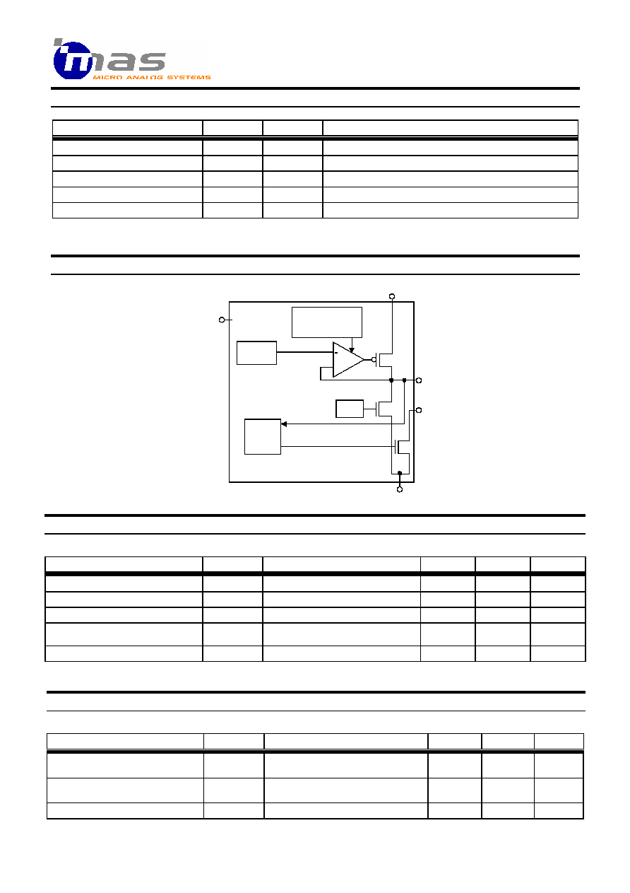
BLOCK DIAGRAM
ABSOLUTE MAXIMUM RATINGS
All voltages with respect to ground.
Parameter
Symbol
Conditions
Min
Max
Unit
Supply Voltage
V
IN
-0.3
6
V
Voltage Range for All Pins
-0.3
V
IN
+ 0.3
V
ESD Rating
HBM
2
kV
Junction Temperature
T
Jmax
+175
(limited)
∞C
Storage Temperature
T
S
-55
+150
∞C
Stresses beyond those listed may cause permanent damage to the device. The device may not operate under these conditions, but it will
not be destroyed.
RECOMMENDED OPERATING CONDITIONS
All voltages with respect to ground.
Parameter
Symbol
Conditions
Min
Max
Unit
Operating Junction
Temperature
T
J
-40
+125
∞C
Operating Ambient
Temperature
T
A
-40
+85
∞C
Operating Supply Voltage
V
IN
2.5
5.3
V
G = Ground, I = Input, O = Output, P = Power
EN
VIN
VOUT
GND
OVER CURRENT /
OVER TEMPERATURE
PROTECTION
VOLTAGE
REFERENCE
+
POWER
GOOD
CONTROL
SHUT
DOWN
PG
DA9165.001
7 October 2002
3 (10)
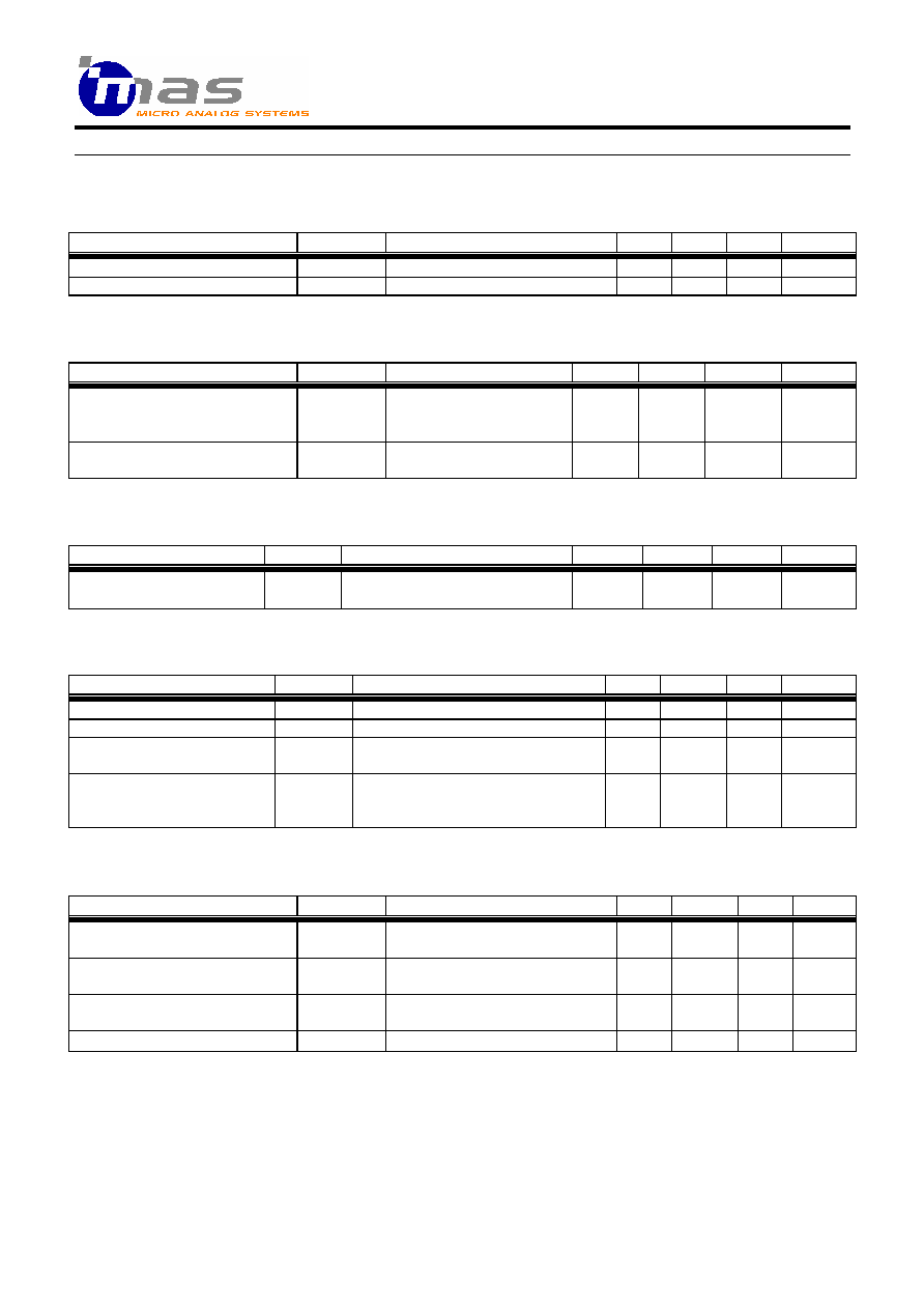
ELECTRICAL CHARACTERISTICS
x
Thermal Protection
T
J
= -40∞C to +125∞C, typical values at T
J
= +27∞C, V
IN
= 3.6 V, I
OUT
= 1 mA, C
IN
= 1 µF, C
L
= 1.0 µF, V
EN
= V
IN
, unless otherwise specified.
Parameter
Symbol
Conditions
Min
Typ
Max
Unit
High Threshold
T
H
145
160
175
∞C
Low Threshold
T
L
135
150
165
∞C
x
Control Terminal Specifications
T
J
= -40∞C to +125∞C, typical values at T
J
= +27∞C, V
IN
= 3.6 V, I
OUT
= 1 mA, C
IN
= 1 µF, C
L
= 1.0 µF, V
EN
= V
IN
, unless otherwise specified.
Parameter
Symbol
Conditions
Min
Typ
Max
Unit
Enable Input Voltage
OFF State
ON State
V
EN
-0.3
1.6
0.55
V
IN
+ 0.3
V
Enable Input Current
I
EN
V
EN
= V
IN
V
EN
= 0 V
0
0
µA
x
Voltage Parameters
T
J
= -40∞C to +125∞C, typical values at T
J
= +27∞C, V
IN
= 3.6 V, I
OUT
= 1 mA, C
IN
= 1 µF, C
L
= 1.0 µF, V
EN
= V
IN
, unless otherwise specified.
Parameter
Symbol
Conditions
Min
Typ
Max
Unit
Output Voltage Tolerance
V
OUT
2.5 V
V
IN
5.3 V,
I
OUT
= 0.1 mA
-3
+3
%
x
Current Parameters
T
J
= -40∞C to +125∞C, typical values at T
J
= +27∞C, V
IN
= 3.6 V, I
OUT
= 1 mA, C
IN
= 1 µF, C
L
= 1.0 µF, V
EN
= V
IN
, unless otherwise specified.
Parameter
Symbol
Conditions
Min
Typ
Max
Unit
Continuous Output Current
I
OUT
150
mA
Short Circuit Current
I
MAX
R
L
= 0
420
mA
Ground Pin Current
I
GND
I
OUT
= 0 mA, V
EN
= V
IN
I
OUT
= 150 mA, V
EN
= V
IN
125
205
200
400
µA
Shutdown Current
I
SD
V
EN
= 0 V, Without PG pin current
T
J
= +27∞C
T
J
= +85∞C
0.005
1
5
µA
x
Power Good Specifications
T
J
= -40∞C to +125∞C, typical values at T
J
= +27∞C, V
IN
= 3.6 V, I
OUT
= 1 mA, C
IN
= 1 µF, C
L
= 1.0 µF, V
EN
= V
IN
, unless otherwise specified.
Parameter
Symbol
Conditions
Min
Typ
Max
Unit
Power Good Threshold
(see figure 9, p. 6)
V
PGL
V
PGH
% of V
OUT
(PG ON)
% of V
OUT
(PG OFF)
89.5
96.5
%
Power Good Output: Logic
Low Voltage
V
PNG
Fault condition, I
PG
= 100 µA
0.02
0.1
V
Power Good Output: Leakage
Current
I
PGLK
Power OK, V
PG
= 5.3 V
0.002
0.1
µA
Delay Time To Power Good
t
PGD
1
2
5
ms

DA9165.001
7 October 2002
4 (10)
x
Power Dissipation
T
J
= -40∞C to +125∞C, typical values at T
J
= +27∞C, V
IN
= 3.6 V, I
OUT
= 1 mA, C
IN
= 1 µF, C
L
= 1.0 µF, V
EN
= V
IN
, unless otherwise specified.
Parameter
Symbol
Conditions
Min
Typ
Max
Unit
Thermal Resistance
(Junction-to-Air)
R
JA
Typical PC board mounting,
still air
255.9
∞C/W
Maximum Power Dissipation
P
d
any ambient temperature
JA
A
(MAX)
J
MAX
d
R
T
T
P
-
=
W
Note 1
Note 1
: T
J(MAX)
denotes maximum operating junction temperature (+125∞C), T
A
ambient temperature, and R
JA
junction-to-air thermal
resistance (+255.9∞C/W).
x
Line and Load Regulation
T
J
= -40∞C to +125∞C, typical values at T
J
= +27∞C, V
IN
= 3.6 V, I
OUT
= 1 mA, C
IN
= 1 µF, C
L
= 1.0 µF, V
EN
= V
IN
, unless otherwise specified.
Parameter
Symbol
Conditions
Min
Typ
Max
Unit
Line Regulation
V
IN
= 2.5 V to 5.3 V
-0.3
0.3
%/V
Load Regulation
I
OUT
= 0.1 mA to 150 mA
5
%
x
Noise and Ripple Rejection
T
J
= -40∞C to +125∞C, typical values at T
J
= +27∞C, V
IN
= 3.6 V, I
OUT
= 1 mA, C
IN
= 1 µF, C
L
= 1.0 µF, V
EN
= V
IN
, unless otherwise specified.
Parameter
Symbol
Conditions
Min
Typ
Max
Unit
Output Noise Voltage
V
RMS
300 Hz < f < 50 kHz
V
OUT
= 0.9 V
V
OUT
= 1.2 V
10 Hz < f < 1 MHz
V
OUT
= 0.9 V
V
OUT
= 1.2 V
44
57
55
73
µVrms
Output Noise Density
V
N
I
OUT
= 150 mA,
f = 1 kHz
255
nV/ Hz
PSRR
I
OUT
= 150 mA
f = 120 Hz
f = 1 kHz
f = 10 kHz
60
60
55
dB
x
Dynamic Parameters
T
J
= -40∞C to +125∞C, typical values at T
J
= +27∞C, V
IN
= 3.6 V, I
OUT
= 1 mA, C
IN
= 1 µF, C
L
= 1.0 µF, V
EN
= V
IN
, unless otherwise specified.
Parameter
Symbol
Conditions
Min
Typ
Max
Unit
Turn-ON Time
(see figure 1 below)
t
ON
I
OUT
= 0 mA,
V
OUT
from 1% to 99%
15
µs
Turn-OFF Time
t
OFF
I
OUT
= 0 mA,
V
OUT
from 99% to 1%
60
µs
Start-up Delay
(see figure 1 below)
V
EN
= 0 V to V
IN
, I
OUT
= 150 mA
23
µs
Overshoot
V
EN
= 0 V to V
IN
15
%
Figure 1.
Definitions of
turn-ON time, overshoot
and start-up delay.
EN
VOUT
50%
start-up delay
90%
overshoot
turn-ON time
99%
1%
DA9165.001
7 October 2002
5 (10)
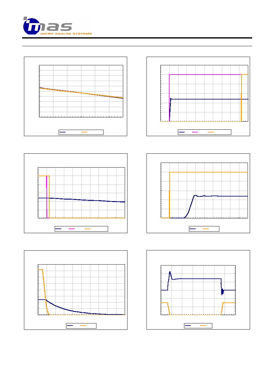
TYPICAL PERFORMANCE CHARACTERISTICS
DUT = MAS9165ASTS, V
IN
= 2.5 V, T
A
= +27∞C, I
OUT
= 10 mA, C
IN
= 1.0 µF, C
L
= 1.0 µF, V
EN
= V
IN
, unless otherwise specified.
MAS9165 Load regulation
1.1
1.12
1.14
1.16
1.18
1.2
1.22
1.24
1.26
1.28
1.3
0
25
50
75
100
125
150
Load current (mA)
O
u
t
p
ut
vo
l
t
ag
e
(
V
)
Vin = 3.6 V
Vin = 2.5 V
MAS9165 Power Good Function during start-up
0
0.5
1
1.5
2
2.5
3
Time (200 µs/div)
V
o
l
t
ag
e (
V
)
Vout
Enable
Power Good
Figure 2.
Load regulation.
Figure 3.
Power Good Function during start-up.
MAS9165 Power Good Function during
shutdown
0
0.5
1
1.5
2
2.5
3
Time (500 ns/div)
V
o
l
t
age (
V
)
Vout
Enable
Power Good
MAS9165 Enable response, I
OUT
= 90 mA
0
0.5
1
1.5
2
2.5
3
Time (5 µs/div)
Vo
lt
a
g
e
(
V
)
Vout
Enable
Figure 4.
Power Good Function during shutdown.
Figure 5.
Enable response. I
OUT
= 90 mA.
MAS9165 Shutdown without Power Good,
V
IN
= 3.6 V
0
0.5
1
1.5
2
2.5
3
3.5
4
Time (5 µs/div)
V
o
l
t
age (
V
)
Vout
Enable
MAS9165 Load transient response, V
IN
= 3.6 V,
V
OUT
= 1.2 V
-60
-40
-20
0
20
40
60
Time (50 µs/div)
O
u
t
put
v
o
l
t
a
g
e
0
100
200
300
400
500
600
O
u
tp
u
t
c
u
rr
e
n
t (m
A
)
Vout
Iout
Ou
t
p
u
t
v
o
l
t
ag
e
ch
an
g
e
(
m
V
)
Figure 6.
Shutdown without Power Good.
Figure 7.
Load transient response. I
OUT
= 150...1 mA, 10 µs
fall/rise time, V
OUT
= 1.2 V.