 | –≠–ª–µ–∫—Ç—Ä–æ–Ω–Ω—ã–π –∫–æ–º–ø–æ–Ω–µ–Ω—Ç: MAS9186 | –°–∫–∞—á–∞—Ç—å:  PDF PDF  ZIP ZIP |

1 (9)
DA9186.000
22 May, 2002
MAS9186
8 X 8-bit D to A Converter
∑
3-pin Serial Data Interface
∑
Low Voltage Output Buffer
DESCRIPTION
MAS9186 is 8-channel 8-bit DAC, designed
primarily for trimmer replacement. Device is
controlled by a simple 3-line input. The output
buffers operate in the entire voltage range from
ground to the positive power supply rail.
DAC is selected with three first bits in serial input
data (SDI-pin) and the DAC output value is set
according to the last 8 bits in serial input data.
FEATURES
APPLICATIONS
∑
Eight 8-bit DACs on a single monolithic chip
∑
Voltage level output
∑
TSSOP 16 package
∑
Single +2.7V supply
∑
Power-on
reset
∑
High resolution monitors
∑
Automatic gain control
∑
Trimmer
replacement
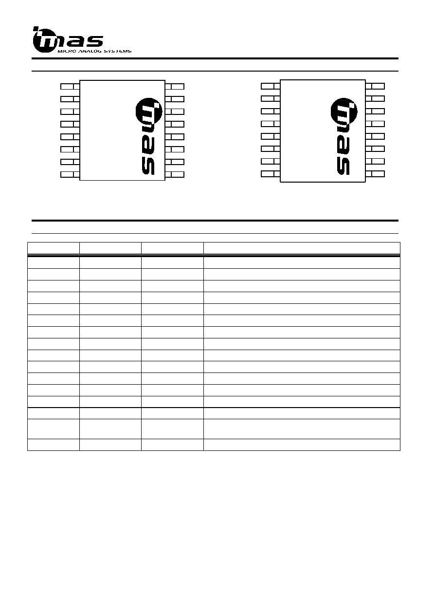
BLOCK DIAGRAM
This is preliminary information on a new
product under development. Micro Analog
Systems Oy reserves the right to make any
changes without notice.
8-BIT DAC
8-BIT DAC
8-BIT DAC
8-BIT DAC
8-BIT DAC
8-BIT DAC
O4
8-BIT DAC
O3
O2
O1
VREFH
8-BIT DAC
O8
O7
O6
O5
CLK
SDI
XCS
VDD
GND
11-bit
Shift
Register
Address
Decoder
8-bit data
MAS9186A2
VREFL
(XRESET in
MAS9186A1)
2 (9)
DA9186.000
22 May, 2002
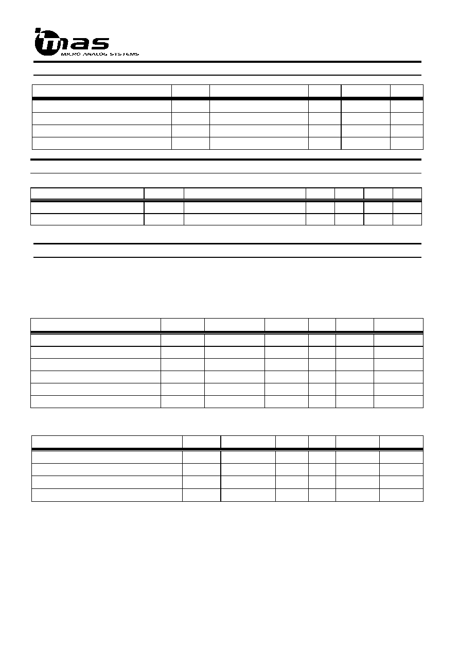
PIN CONFIGURATION
PIN DESCRIPTION
Pin Number
MAS9186 A1
MAS9186 A2
Function
1
VREFH
VREFH
DAC output reference high voltage
2
O1
O1
DAC 1, address 0x0
3
O2
O2
DAC 2, address 0x1
4
O3
O3
DAC 3, address 0x2
5
O4
O4
DAC 4, address 0x3
6
O5
O5
DAC 5, address 0x4
7
O6
O6
DAC 6, address 0x5
8
XSHDN
XSHDN
Device analog part power-down signal (active low)
9
XCS
XCS
Device enable signal (rising edge loads data to DAC)
10
GND
GND
Device ground-pin
11
CLK
VREFL
Data clock / DAC output low reference voltage
12
SDI
CLK
Serial input data / Data clock
13
O7
SDI
DAC 7, address 0x6 / Serial input data
14
O8
O7
DAC 8, address 0x7 / DAC 7, address 0x6
15
XRESET
O8
Device Digital part reset ≠ middle code preset pin/DAC 8,
address 0xB
16
VDD
VDD
Device power supply pin
MAS9186 has two bonding options available:
∑
MAS9186A1, where VREFL pin is bonded to GND pin and XRESET pin can be used
∑
MAS9186A2, where XRESET pin is bonded to VDD pin and VREFL pin can be used
VREFH
VREFH
1
2
3
4
5
6
7
8
9
10
11
12
13
14
15
16
1
2
3
4
5
6
7
8
9
10
11
12
13
14
15
16
O1
O2
O3
O4
O5
O6
XSHDN
XCS
GND
O1
O2
O3
O4
O5
O6
XSHDN
XCS
GND
M
A
S
9
1
8
6
A
1
M
A
S
9
1
8
6
A
2
VDD
XRESET
08
O7
SDI
CLK
VDD
VREFL
O8
O7
SDI
CLK
Top view
Y
Y
W
W
Y
Y
W
W
YYWW = year, week
3 (9)
DA9186.000
22 May, 2002
ABSOLUTE MAXIMUM RATINGS
Parameter
Symbol
Conditions
Min
Max
Unit
Power Supply (VDD to GND)
VDD
-0.3
+6.0
V
Input Voltage Range (any other pin)
-0.3
VDD + 0.3
V
Continuous Power Dissipation
1000
mW
Storage Temperature Range
-65
+150
∞
C
RECOMMENDED OPERATION CONDITIONS
Parameter
Symbol
Conditions
Min
Typ
Max
Unit
Supply Voltage Range
VDD
2.7
3.6
5.5
V
Operating Temperature Range
Temp
-40
+85
∞
C
ELECTRICAL CHARACTERISTICS
(VDD = 3.0 V
±
10% or 5.0 V
±
10%, VREFH = VDD, VREFL = 0V, -40
∞
C
T
A
+85
∞
C unless otherwise noted)
DC Parameters
x
Digital Inputs
Parameter
Symbol
Conditions
Min
Typ
Max
Unit
DAC Resolution
N
8
Bits
DAC Differential Nonlinearity Error
DNL
-1
+1
LSB
DAC Integral Nonlinearity Error
INL
-1
+1
LSB
DAC Full-scale Error
GFSE
-1
+1
LSB
DAC Zero Code Error
BZSE
-1
+1
LSB
DAC Output Resistance
ROUT
30
60
x
Reference Input
Parameter
Symbol
Conditions
Min
Typ
Max
Unit
REFH Voltage Range
VREFH
V
REFH
> V
REFL
0
VDD
REFL Voltage Range (MAS9186A2 only)
VREFL
V
REFH
> V
REFL
0
VDD
REFH Input Resistance
RREFH
5
10
k
REFL Input Resistance
RREFL
10
k
4 (9)
DA9186.000
22 May, 2002
x
Digital Input
Parameter
Symbol
Conditions
Min
Typ
Max
Unit
Digital Logic High
VIH
0.7*VDD
Digital Logic Low
VIL
0.3*VDD
Digital Input Current
IIL
±
1
uA
x
Power Supplies
Parameter
Symbol
Conditions
Min
Typ
Max
Unit
Power Supply Range
VDD
2.7
5.5
V
Supply Current
IDD
VDD = 3.60V
3
6
mA
Supply Current
IDD
VDD = 5.50V
20
mA
Shutdown Current
ISHDN
0.5
5
uA
AC Parameters
x
AC Characteristics
Dynamic Performance
Parameter
Symbol
Conditions
Min
Typ
Max
Unit
Power Supply Sensitivity (100Hz)
PSRR
54
dB
Vout Settling time (
±
1/2 LSB error band)
TS
6
µ
s
Crosstalk between adjacent outputs
CT
63
dB
Switching Characteristics
(Minimum values at +25
o
C, VDD = 3.60 V)
Parameter
Symbol
Conditions
Min
Typ
Max
Unit
Input Clock High Pulse Width
TCH
16
ns
Input Clock Low Pulse Width
TCL
7
ns
Data Setup Time
TDS
-5
ns
Data Hold Time
TDH
5
ns
XCS Fall to First Clock Pulse Fall
TCLCL
16
ns
XCS High Pulse Width
TCSW
22
ns
RESET Pulse Width
TRS
28
ns
CLK Rise to XCS Rise Hold Time
TCSH
22
ns
XCS Rise to CLOCK Rise Setup
TCS1
-5
ns

5 (9)
DA9186.000
22 May, 2002
OPERATING MODES
DAC maximum output voltage is set using VREFH and VREFL pins (= 255/256 * (VREFH-VREFL)+VREFL)
(note: VREFL=GND in case of MAS9186A1). XRESET pin is used for middle code preset: DAC registers are
reset and middle code will appear at the DAC output.
Serial input data is written to SDI while XCS is low. Data is read at CLK rising edge to on-chip shift register.
Rising XCS-pin stops data reading and 11 CLK-cycles are used as the input data (3 address bits and 8 data bits).
The last 11 bits before rising XCS are used as input data.
x
Timing diagram
APPLICATION AND TEST CIRCUIT INFORMATION
Clock
Data In
MAS9186A2
O8
O1
O2
O3
O4
O5
O6
O7
15
14
7
6
5
4
3
2
VREFH
VREFL
CLK
SDI
12
13
Controller
VDD
GND
+3.0v
11
10
1
16
XCS
Latch
9
8
XSHDN
100 nF
CLK
XCS
DAC Register Load
V
OUT
SDI
A2 A1 A0 D7 D6 D5 D4 D3 D2 D1 D0