 | ÐлекÑÑоннÑй компоненÑ: DS1882 | СкаÑаÑÑ:  PDF PDF  ZIP ZIP |
DS1882 DS
General Description
The DS1882 is a dual, nonvolatile (NV) digital poten-
tiometer designed to operate in audio systems that
accomodate up to ±7V signal levels. The potentiometer
settings can be stored in EEPROM so that they are
retained when the power is cycled. The DS1882 has
separate supplies for the potentiometers (V
CC
) and the
communication circuitry (V
DD
). For clickless/popless
operation, a zero-crossing detector allows the wiper
position to change when there is no voltage across the
potentiometer. The DS1882 is also designed to mini-
mize crosstalk, and the two digital potentiometers pro-
vide 0.5dB channel-to-channel matching to prevent
volume differences between channels. Total harmonic
distortion (THD) is also minimal as long as the wiper
drives a high-impedance load.
Two attenuation configuration options provide optimum
flexibility for the specific application. Configuration
Option 1 provides 63 logarithmic tapered steps (0dB to
-62dB, 1dB/step) plus a mute setting. Configuration
Option 2 has 32 logarithmic steps plus mute and pro-
vides software compatibility with the DS1808. When
Configuration Option 2 is used in combination with the
16-pin SO package, the DS1882 is both software and pin
compatible with the DS1808 in 5V applications.
Applications
Notebook and PC Audio
Portable Audio Equipment
Car Stereo
Consumer Audio/Video
Features
o Dual, Audio Log Taper Potentiometers
o Low THD+N and Crosstalk
o ±7V Analog Supply (Independent of Digital
Supply)
o 5V Digital Supply
o Potentiometer Settings Configurable as
Nonvolatile or Volatile
o Zero-Crossing Detector Eliminates Switching
Noise
o Two User-Configurable Attenuation Options
o Configuration Option 1: 63 Positions Provide 1dB
Attenuation Steps from 0dB to -62dB Plus Mute
o Configuration Option 2: (Software-Compatible
with the DS1808): 33 Positions Plus Mute as
Follows
Positions 012: 1dB per Step for 12 Steps
Positions 1324: 2dB per Step for 12 Steps
Positions 2532: 3dB per Step for 8 Steps
o I
2
C*-Compatible Serial Interface
o Three Address Pins Allow Up to 8 Devices on
I
2
C Bus
o 45k Potentiometer End-to-End Resistance
o Industrial Temperature Range (-40°C to +85°C)
o 16-Pin TSSOP or SO Package
DS1882
Dual Log Audio Digital Potentiometer
______________________________________________ Maxim Integrated Products
1
16
15
14
13
12
11
10
1
2
3
4
5
6
7
V
DD
V
CC
SCL
SDA
V-
A1
A2
GND
TOP VIEW
CE
W1
H1
L0
W0
9
8
L1
H0
A0
TSSOP/SO
DS1882
+
Pin Configuration
Rev 0; 6/06
For pricing, delivery, and ordering information, please contact Maxim/Dallas Direct! at
1-888-629-4642, or visit Maxim's website at www.maxim-ic.com.
+Denotes lead-free package.
Ordering Information
PART
TEMP
RANGE
VERSION
(k
)
PIN-
PACKAGE
DS1882E-050+
-40°C to +85°C
45
16 TSSOP
(173 mils)
DS1882E-050+T&R -40°C to +85°C
45
16 TS S O P
( 173 m i l s)
Tap e- and - Reel
DS1882Z-050+
-40°C to +85°C
45
16 S O
( 150 m i l s)
DS1882Z-050+T&R -40°C to +85°C
45
16 S O
( 150 m i l s)
Tap e- and - Reel
Purchase of I
2
C components from Maxim Integrated Products, Inc., or one of its sublicensed Associated Companies, conveys a
license under the Philips I
2
C Patent Rights to use these components in an I
2
C system, provided that the system conforms to the I
2
C
Standard Specification as defined by Philips.
Typical Operating Circuit appears at end of data sheet.
DS1882
Dual Log Audio Digital Potentiometer
2
_____________________________________________________________________
ABSOLUTE MAXIMUM RATINGS
RECOMMENDED OPERATING CONDITIONS
(T
A
= -40°C to +85°C)
Stresses beyond those listed under "Absolute Maximum Ratings" may cause permanent damage to the device. These are stress ratings only, and functional
operation of the device at these or any other conditions beyond those indicated in the operational sections of the specifications is not implied. Exposure to
absolute maximum rating conditions for extended periods may affect device reliability.
Voltage on V
DD
, SDA, and SCL Relative to GND .....-0.5V to +6.0V
Voltage on A2, A1, A0, and CE Relative
to GND .................-0.5V to (V
DD
+ 0.5V), not to exceed +6.0V
Voltage on V
CC
Relative to GND ...........................-0.5V to +8.0V
Voltage on H1, H0, W1, W0, L1, and L0 Relative
to GND ............................................(V- - 0.5V) to (V
CC
+ 0.5V)
Voltage on V- Relative to GND ..............................-8.0V to +0.5V
Maximum Resistor Current .................................................±3mA
Operating Temperature Range ...........................-40°C to +85°C
Programming Temperature Range .........................0°C to +70°C
Storage Temperature Range .............................-55°C to +125°C
Soldering Temperature...................See J-STD-020 Specification
PARAMETER
SYMBOL
CONDITIONS
MIN
TYP
MAX
UNITS
Digital Supply Voltage
V
DD
(Notes 1, 2)
4.5
5.5
V
Analog Supply Range
V
CC
(Notes 1, 2)
4.5
7.0
V
Negative Supply Voltage
V-
(Notes 1, 2)
-7.0
-4.5
V
Potentiometer Voltages
-V
V
CC
V
Wiper Current
±1
mA
DC ELECTRICAL CHARACTERISTICS
(V
DD
= +4.5V to +5.5V, V
CC
= +4.5V to +7.0V, V- = -4.5V to -7.0V, T
A
= -40°C to +85°C.)
PARAMETER
SYMBOL
CONDITIONS
MIN
TYP
MAX
UNITS
Digital Supply Current
I
DD
(Note 3)
0.2
5
µA
Analog Supply Current
I
CC
(Note 4)
2.5
10
µA
Input Logic 0
(CE, SDA, SCL, A0, A1, A2)
V
IL
(Note 5)
-0.3
0.15 x
V
DD
V
Input Logic 1
(CE, SDA, SCL, A0, A1, A2)
V
IH
(Note 5)
0.8 x
V
DD
V
DD
+
0.3
V
I
OL
= 4mA
0.4
Output-Voltage Low (SDA)
V
OL
I
OL
= 6mA
0.6
V
Input Leakage Current
I
LI
-1
+1
µA
I/O Pin Input Current (SDA)
0.4V < V
SDA
< (0.9 x V
DD
)
-10
+10
µA
I/O Capacitance
C
I/O
(Note 6)
10
pF
Power-Up Time
t
PU
1
ms
DS1882
Dual Log Audio Digital Potentiometer
_____________________________________________________________________
3
I
2
C CHARACTERISTICS (See Figure 4)
(V
DD
= +4.5V to +5.5V, V
CC
= +4.5V to +7.0V, V- = -4.5V to -7.0V, T
A
= -40°C to +85°C. Timing referenced to V
IL(MAX)
and V
IH(MIN)
.)
PARAMETER
SYMBOL
CONDITIONS
MIN
TYP
MAX
UNITS
SCL Clock Frequency
f
SCL
(Note 9)
0
400
kHz
Bus Free Time Between STOP and
START Conditions
t
BUF
1.3
µs
Hold Time (Repeated) START Condition
t
HD:STA
0.6
µs
Low Period of SCL
t
LOW
1.3
µs
High Period of SCL
t
HIGH
0.6
µs
Data Hold Time
t
HD:DAT
0
0.9
µs
Data Setup Time
t
SU:DAT
200
ns
START Setup Time
t
SU:STA
0.6
µs
SDA and SCL Rise Time
t
R
(Note 10)
20 +
0.1C
B
300
ns
SDA and SCL Fall Time
t
F
(Note 10)
20 +
0.1C
B
300
ns
STOP Setup Time
t
SU:STO
0.6
µs
SDA and SCL Capacitive Loading
C
B
(Note 10)
400
pF
EEPROM Write Time
t
W
(Note 11)
5
10
ms
ANALOG POTENTIOMETER CHARACTERISTICS
(V
DD
= +4.5V to +5.5V, V
CC
= +4.5V to +7.0V, V- = -4.5V to -7.0V, T
A
= -40°C to +85°C.)
PARAMETER
SYMBOL
CONDITIONS
MIN
TYP
MAX
UNITS
End-to-End Resistance
R
EE
+25°C
45
k
End-to-End Resistance Tolerance
+25°C
-20
+20
%
Ratiometric Temperature Coefficient
(Note 6)
30
ppm/°C
End-to-End Resistance Temperature
Coefficient
(Note 6)
750
ppm/°C
Wiper Resistance
R
W
160
250
Absolute Attenuation Tolerance
(Note 7)
-0.5
+0.5
dB
Mute Position Attenuation
100
dB
Step Size Deviation from Nominal
(Note 7)
-0.25
+0.25
dB
Interchannel Matching
(Note 7)
-0.5
+0.5
dB
-3dB Cutoff Frequency
10pF load
5
MHz
Output Noise
20Hz to 20kHz, grounded input,
tap = -6dB
2.2
µV
RMS
Crosstalk
1kHz, grounded input, tap = -6dB
-120
dB
THD+N
1kHz, tap = -6dB, C
L
= 10pF
(Note 8)
0.005
%
Zero-Crossing Detection
t
ZCD
38
50
ms
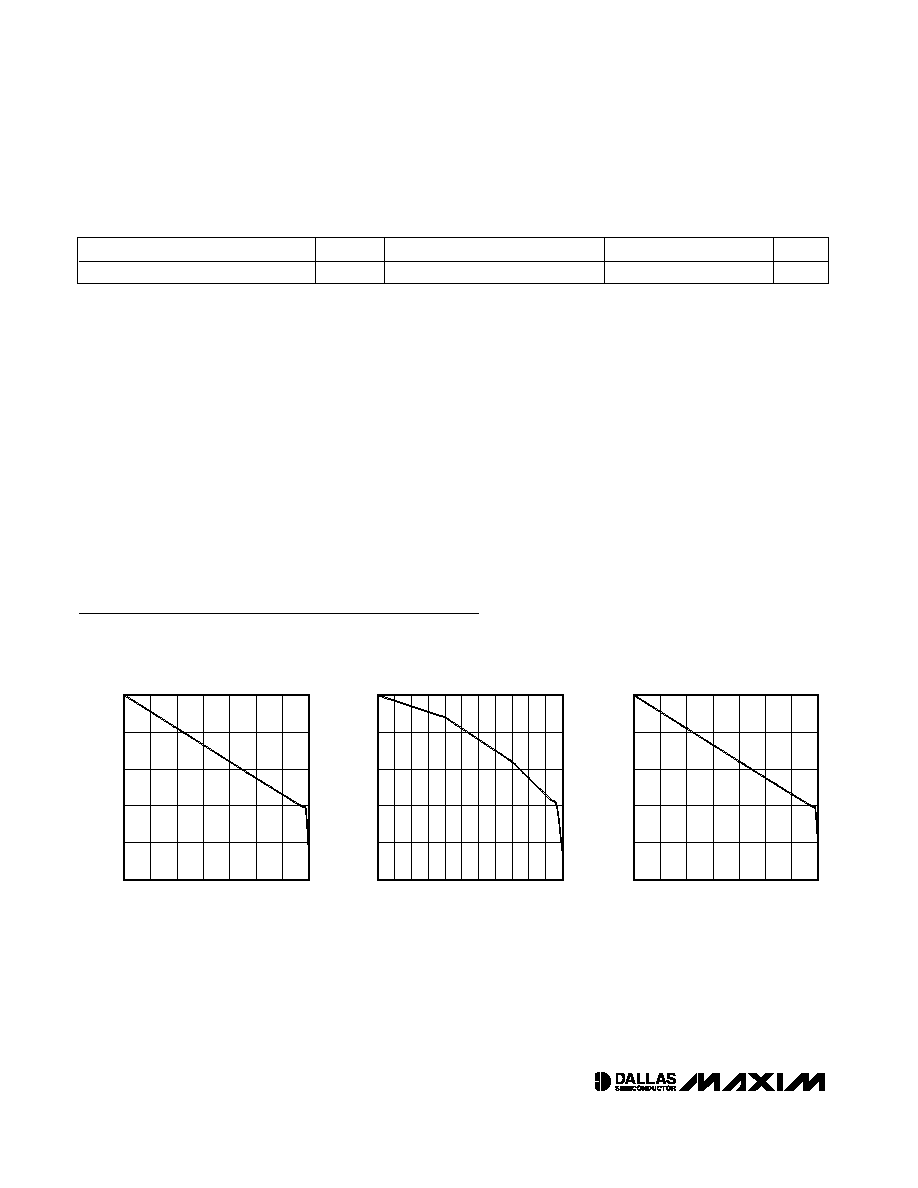
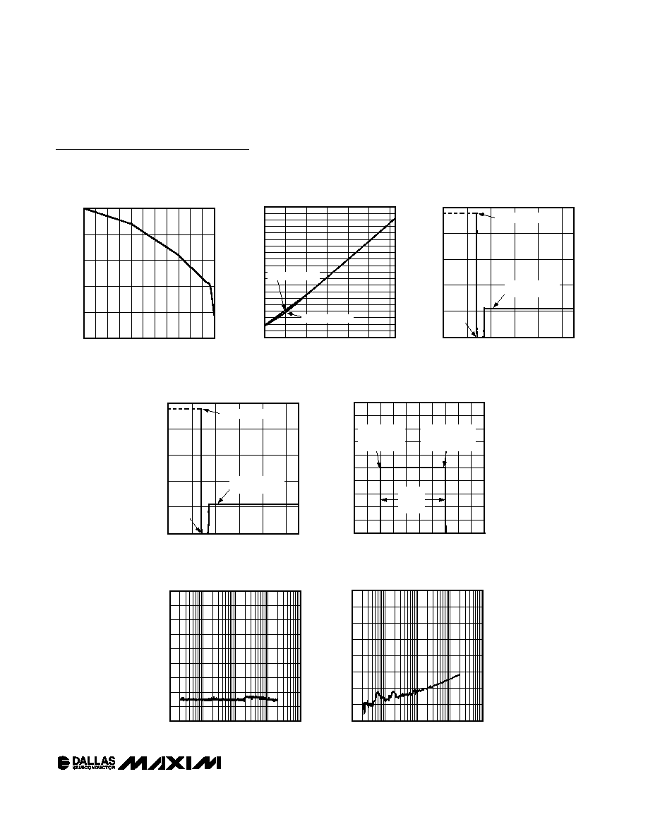
POTENTIOMETER 0 (CONFIGURATON 1)
ATTENUATION vs. SETTING
DS1882 toc01
SETTING (DEC)
ATTENUATION (dB)
54
45
36
27
18
9
-80.0
-60.0
-40.0
-20.0
0
-100.0
0
63
POTENTIOMETER 0 (CONFIGURATON 2)
ATTENUATION vs. SETTING
DS1882 toc02
SETTING (DEC)
ATTENUATION (dB)
30
24
18
12
6
-80.0
-60.0
-40.0
-20.0
0
-100.0
0
33
27
21
15
9
3
POTENTIOMETER 1 (CONFIGURATON 1)
ATTENUATION vs. SETTING
DS1882 toc03
SETTING (DEC)
ATTENUATION (dB)
54
36
18
-80.0
-60.0
-40.0
-20.0
0
-100.0
0
63
45
27
9
DS1882
Dual Log Audio Digital Potentiometer
4
_____________________________________________________________________
NV MEMORY CHARACTERISTICS
(V
DD
= +4.5V to +5.5V, V
CC
= +4.5V to +7.0V, V- = -4.5V to -7.0V, T
A
= 0°C to +70°C.)
PARAMETER
SYMBOL
CONDITIONS
MIN
TYP
MAX
UNITS
Writes
+70°C (Note 6)
50,000
Note 1:
All voltages are referenced to ground.
Note 2:
The value of V
DD
should never exceed V
CC
, including during power-ups. V
CC
must be applied before V
DD
.
Note 3:
I
DD
is specified with SDA = SCL = CE = V
DD
, resistor pins floating, and digital inputs connected to V
DD
or GND.
Note 4:
I
CC
is specified with SDA = SCL = CE = V
DD
, resistor pins floating, and digital inputs connected to V
DD
or GND, after zero-
crossing detection has timed out.
Note 5:
The DS1882 will not obstruct the SDA and SCL lines if V
DD
is switched off as long as the voltages applied to these inputs
do not violate their minimum and maximum input voltage levels.
Note 6:
Guaranteed by design.
Note 7:
Above Position 50, these are typical maximum. Guaranteed by characterization.
Note 8:
Load is representative of the input of a low-noise audio amp.
Note 9:
Timing shown is for fast-mode (400kHz) operation. This device is also backward-compatible with I
2
C standard-mode timing.
Note 10: C
B
--Total capacitance of one bus line in picofarads.
Note 11: If zero-crossing detection is enabled, the EEPROM write does not begin until the current zero-crossing detection is com-
plete. Otherwise, EEPROM write begins after a STOP condition occurs.
Typical Operating Characteristics
(V
DD
= V
CC
= +5.0V, V- = -5.0V, T
A
= +25°C.)
DS1882
Dual Log Audio Digital Potentiometer
_____________________________________________________________________
5
POTENTIOMETER 1 (CONFIGURATON 2)
ATTENUATION vs. SETTING
DS1882 toc04
SETTING (DEC)
ATTENUATION (dB)
30
24
18
12
6
-80.0
-60.0
-40.0
-20.0
0
-100.0
0
33
27
21
15
9
3
END-TO-END RESISTANCE PERCENT
CHANGE FROM +25
°C vs. TEMPERATURE
TEMPERATURE (
°C)
RESISTANCE % CHANGE (FROM +25
°
C)
DS1882 toc05
-40
-20
0
20
40
60
80
-5.0
-4.5
-4.0
-3.5
-3.0
-2.5
-2.0
-1.5
-1.0
-0.5
0
0.5
1.0
1.5
2.0
2.5
3.0
3.5
4.0
4.5
5.0
POTENTIOMETER 1
POTENTIOMETER 0
RESISTANCE vs. POWER-UP VOLTAGE
DS1882 toc06
POWER-UP VOLTAGE (V)
RESISTANCE (k
)
5
4
3
2
1
20
40
60
80
100
0
0
PROGRAMMED
RESISTANCE (6dBh)
MUTE
HIGH IMPEDANCE
RESISTANCE
vs. POWER-DOWN VOLTAGE
DS1882 toc07
POWER-DOWN VOLTAGE (V)
RESISTANCE (k
)
5
4
3
2
1
20
40
60
80
100
0
0
PROGRAMMED
RESISTANCE (6dBh)
MUTE
HIGH IMPEDANCE
I
CC
vs. ZERO-CROSSING TIMING
DS1882 toc08
TIME (ms)
I
CC
(
µ
A)
100
200
300
400
500
600
700
800
900
1000
0
ZERO-CROSSING
TIMEOUT OR ZERO-
CROSSING EVENT
ZERO-CROSSING
DETECTION
ACTIVATED
TYPICAL
TIMEOUT
OF 50ms
CROSSTALK vs. FREQUENCY (-6dB)
FREQUENCY (kHz)
CROSSTALK (dB)
DS1882 toc10
-160
-140
-120
-100
-80
-60
-40
-20
0
0.01
0.10
1.00
10.00
100.00
Typical Operating Characteristics (continued)
(V
DD
= V
CC
= +5.0V, V- = -5.0V, T
A
= +25°C.)
THD+N vs. FREQUENCY (0dB)
DS1882 toc09
FREQUENCY (kHz)
THD+N (%)
10.00
1.00
0.10
0.0002
0.0004
0.0006
0.0008
0.0010
0.0012
0.0014
0.0016
0.0018
0
0.01
100.00