 | –≠–ª–µ–∫—Ç—Ä–æ–Ω–Ω—ã–π –∫–æ–º–ø–æ–Ω–µ–Ω—Ç: DS2070W | –°–∫–∞—á–∞—Ç—å:  PDF PDF  ZIP ZIP |

General Description
The DS2070W is a 16Mb reflowable nonvolatile (NV)
SRAM, which consists of a static RAM (SRAM), an NV
controller, and an internal rechargeable manganese
lithium (ML) battery. These components are encased in
a surface-mount module with a 256-ball BGA footprint.
Whenever V
CC
is applied to the module, it recharges the
ML battery, powers the SRAM from the external power
source, and allows the contents of the SRAM to be mod-
ified. When V
CC
is powered down or out-of-tolerance,
the controller write-protects the SRAM's contents and
powers the SRAM from the battery. The DS2070W also
contains a power-supply monitor output, RST, which can
be used as a CPU supervisor for a microprocessor.
Applications
RAID Systems and Servers
POS Terminals
Industrial Controllers
Routers/Switches
Data-Acquisition Systems
Fire Alarms
Gaming
PLC
Features
o Single-Piece, Reflowable, (27mm)
2
PBGA Package
Footprint
o Internal ML Battery and Charger
o Unconditionally Write-Protects SRAM when V
CC
is Out-of-Tolerance
o Automatically Switches to Battery Supply when
V
CC
Power Failures Occur
o Internal Power-Supply Monitor Detects Power Fail
Below Nominal V
CC
(3.3V)
o Reset Output can be Used as a CPU Supervisor
for a Microprocessor
o Industrial Temperature Range (-40∞C to +85∞C)
o UL Recognized
DS2070W
3.3V Single-Piece 16Mb
Nonvolatile SRAM
______________________________________________ Maxim Integrated Products
1
Rev 0; 8/06
For pricing, delivery, and ordering information, please contact Maxim/Dallas Direct! at
1-888-629-4642, or visit Maxim's website at www.maxim-ic.com.
Ordering Information
Pin Configuration appears at end of data sheet.
PART
TEMP RANGE
PIN-PACKAGE
SPEED (ns)
SUPPLY TOLERANCE
DS2070W-100#
-40∞C to +85∞C
256 Ball (27mm)
2
BGA Module
100
3.3V ±0.3V
Typical Operating Circuit
(CE)
DATA
ADDRESS
(INT)
RST
A0≠A20
DQ0≠DQ7
CE
21 BITS
8 BITS
MICROPROCESSOR
OR DSP
DS2070W
2048k x 8
NV SRAM
(WR)
WE
(RD)
OE
#Denotes a RoHS-compliant device that may include lead that is exempt under the RoHS requirements.

DS2070W
3.3V Single-Piece 16Mb
Nonvolatile SRAM
2
_____________________________________________________________________
ABSOLUTE MAXIMUM RATINGS
RECOMMENDED OPERATING CONDITIONS
(T
A
= -40
∞C to +85∞C.)
Stresses beyond those listed under "Absolute Maximum Ratings" may cause permanent damage to the device. These are stress ratings only, and functional
operation of the device at these or any other conditions beyond those indicated in the operational sections of the specifications is not implied. Exposure to
absolute maximum rating conditions for extended periods may affect device reliability.
Voltage on Any Pin Relative to Ground .................-0.3V to +4.6V
Operating Temperature Range ...........................-40∞C to +85∞C
Storage Temperature Range ...............................-40∞C to +85∞C
Soldering Temperature .....................See IPC/JEDEC J-STD-020
PARAMETER
SYMBOL
CONDITIONS
MIN
TYP
MAX
UNITS
Supply Voltage
V
CC
3.0
3.3
3.6
V
Input Logic 1
V
IH
2.2
V
CC
V
Input Logic 0
V
IL
0
0.4
V
DC ELECTRICAL CHARACTERISTICS
(V
CC
= 3.3V ±0.3V, T
A
= -40
∞C to +85∞C.)
PARAMETER
SYMBOL
CONDITIONS
MIN
TYP
MAX
UNITS
Input Leakage Current
I
IL
-1.0
+1.0
µA
I/O Leakage Current
I
IO
CE = V
CC
-1.0
+1.0
µA
Output-Current High
I
OH
At 2.4V
-1.0
mA
Output-Current Low
I
OL
At 0.4V
2.0
mA
Output-Current Low
RST
I
OL
RST
At 0.4V (Note 1)
10.0
mA
I
CCS1
CE = 2.2V
0.5
7
Standby Current
I
CCS2
CE = V
CC
- 0.2V
0.2
5
mA
Operating Current
I
CCO1
t
RC
= 200ns, outputs open
50
mA
Write-Protection Voltage
V
TP
2.8
2.9
3.0
V
AC ELECTRICAL CHARACTERISTICS
(V
CC
= 3.3V ±0.3V, T
A
= -40
∞C to +85∞C.)
PARAMETER
SYMBOL
CONDITIONS
MIN
MAX
UNITS
Read Cycle Time
t
RC
100
ns
Access Time
t
ACC
100
ns
OE to Output Valid
t
OE
50
ns
CE to Output Valid
t
CO
100
ns
CAPACITANCE
(T
A
= +25
∞C.)
PARAMETER
SYMBOL
CONDITIONS
MIN
TYP
MAX
UNITS
Input Capacitance
C
IN
Not tested
7
pF
Input/Output Capacitance
C
OUT
Not tested
7
pF

DS2070W
3.3V Single-Piece 16Mb
Nonvolatile SRAM
_____________________________________________________________________
3
POWER-DOWN/POWER-UP TIMING
(T
A
= -40
∞C to +85∞C.)
PARAMETER
SYMBOL
CONDITIONS
MIN
TYP
MAX
UNITS
V
CC
Fail Detect to
CE and WE Inactive
t
PD
(Note 7)
1.5
µs
V
CC
Slew from V
TP
to 0V
t
F
150
µs
V
CC
Slew from 0V to V
TP
t
R
150
µs
V
CC
Valid to
CE and WE Inactive
t
PU
2
ms
V
CC
Valid to End of Write Protection
t
REC
125
ms
V
CC
Fail Detect to
RST Active
t
RPD
(Note 1)
3.0
µs
V
CC
Valid to
RST Inactive
t
RPU
(Note 1)
225
350
525
ms
DATA RETENTION
(T
A
= +25
∞C.)
PARAMETER
SYMBOL
CONDITIONS
MIN
TYP
MAX
UNITS
Expected Data-Retention Time (Per Charge)
t
DR
(Note 8)
2
3
years
AC ELECTRICAL CHARACTERISTICS (continued)
(V
CC
= 3.3V ±0.3V, T
A
= -40
∞C to +85∞C.)
PARAMETER
SYMBOL
CONDITIONS
MIN
MAX
UNITS
OE or CE to Output Active
t
COE
(Note 2)
5
ns
Output High Impedance from
Deselection
t
OD
(Note 2)
35
ns
Output Hold from Address Change
t
OH
5
ns
Write Cycle Time
t
WC
100
ns
Write Pulse Width
t
WP
(Note 3)
75
ns
Address Setup Time
t
AW
0
ns
t
WR1
(Note 4)
5
Write Recovery Time
t
WR2
(Note 5)
20
ns
Output High Impedance from WE
t
ODW
(Note 2)
35
ns
Output Active from WE
t
OEW
(Note 2)
5
ns
Data Setup Time
t
DS
(Note 6)
40
ns
t
DH1
(Note 4)
0
Data Hold Time
t
DH2
(Note 5)
20
ns
Input Pulse Levels:
V
IL
= 0.0V, V
IH
= 3.0V
Input Pulse Rise and Fall Times:
5ns
Input and Output Timing Reference Level:
1.5V
Output Load:
1 TTL Gate + C
L
(100pF) including scope and jig
AC TEST CONDITIONS

DS2070W
3.3V Single-Piece 16Mb
Nonvolatile SRAM
4
_____________________________________________________________________
Read Cycle
OUTPUT
DATA VALID
t
RC
t
ACC
t
CO
t
OE
t
OH
t
OD
t
OD
t
COE
t
COE
V
IH
V
IH
V
IL
V
OH
V
OL
V
OH
V
OL
V
IL
V
IH
ADDRESSES
CE
OE
D
OUT
(SEE NOTE 9.)
V
IH
V
IH
V
IH
V
IH
V
IL
V
IL
V
IL
DS2070W
3.3V Single-Piece 16Mb
Nonvolatile SRAM
_____________________________________________________________________
5
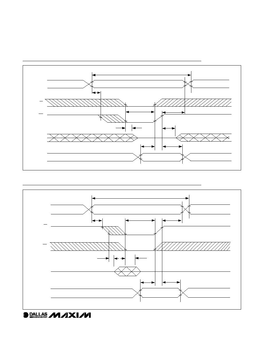
Write Cycle 1
DATA IN STABLE
ADDRESSES
CE
WE
D
OUT
D
IN
t
WC
V
IH
V
IH
V
IH
V
IH
V
IL
V
IL
V
IL
HIGH
IMPEDANCE
V
IH
V
IH
V
IL
V
IL
V
IH
V
IL
V
IL
V
IL
V
IL
t
AW
t
WP
t
OEW
t
DH1
t
DS
t
ODW
t
WR1
(SEE NOTES 2, 3, 4, 6, 10≠13.)
Write Cycle 2
t
WC
t
AW
t
DH2
t
DS
t
COE
t
ODW
t
WP
t
WR2
V
IH
V
IL
V
IH
ADDRESSES
CE
WE
D
OUT
D
IN
V
IL
V
IH
V
IL
V
IH
V
IL
V
IL
V
IL
V
IL
V
IH
V
IH
V
IL
V
IH
DATA IN STABLE
V
IL
V
IL
(SEE NOTES 2, 3, 5, 6, 10≠13.)