
1 of 7
REV: 052604
Note: Some revisions of this device may incorporate deviations from published specifications known as errata. Multiple revisions of any device
may be simultaneously available through various sales channels. For information about device errata, click here:
www.maxim-ic.com/errata
.
GENERAL DESCRIPTION
The DS2125 Ultra3 LVD/SE SCSI terminator is both
a low-voltage differential (LVD) and single-ended
(SE) terminator. The multimode operation enables
the designer to implement LVD in current products
while allowing the end user SE backward
compatibility with legacy devices. If the device is
connected in an LVD-only bus, the DS2125 uses
LVD termination. If any SE devices are connected to
the bus, the DS2125 uses SE termination, which is
accomplished automatically inside the part by
sensing the voltage on the SCSI bus DIFFSENS line.
For the LVD termination, the DS2125 integrates two
current sources with 15 precision resistor strings. For
the SE termination, one regulator and 15 precision
110
W resistors are used. Two DS2125 terminators
are needed for a wide SCSI bus.
APPLICATIONS
Raid Systems
SCSI Host Bus Adapter (HBA) Cards
Servers
SCSI Cables
Network Attached Storage (NAS)
Storage Area Networks (SANs)
FEATURES
�
Fully Compliant with Ultra3 SCSI
�
Provides Multimode Low-Voltage
Differential/Single-Ended (LVD/SE) Termination
for 15 Signal Line Pairs
�
Auto-Selection of LVD or SE Termination
�
5% Tolerance on SE and LVD Termination
Resistance
�
Low 3pF Power-Down Capacitance
�
On-Board Thermal-Shutdown Circuitry
�
SCSI Bus Hot-Plug Compatible
�
Fully Supports Actively Negated SE SCSI
Signals
PIN CONFIGURATION
ORDERING INFORMATION
PART TEMP
RANGE
PIN-PACKAGE
DS2125
0�C to +70�C
48 LQFP
DS2125
Ultra3 LVD/SE SCSI 15-Line Terminator
www.maxim-ic.com
R14N
R14P
R13N
R13P
R12N
R12P
R11N
R11P
R10N
R10P
R9N
R9P
48
47
46
45
44
43
42
41
40
39
38
37
25 26 27 28 29 30
31
32
33
34
35 36
13
14
15
16
17
18
19
20
21
22
23
24
1
2
3
4
5
6
7
8
9
10
11
12
R15P
HS_GND
HS_GND
HS_GND
R15N
TPWR
HS_GND
HS_GND
HS_GND
V
REF
R1P
R1N
R2P
R2N
R3P
R3N
R4P
R4N
R5P
R5N
R6P
R6N
R7P
R7N
HS_GND
HS_GND
HS_GND
ISO
DIFFSENSE
HS_GND
HS_GND
HS_GND
R8P
R8N
GND
DIFF_CAP
Dallas
Semiconductor
DS2125
LQFP
TOP VIEW
DS2125 Ultra3 LVD/SE SCSI 15-Line Terminator
2 of 7
ABSOLUTE MAXIMUM RATINGS
V
REF
, ISO, GND, DIFFSENSE, DIFF_CAP, TPWR, RxP, RxN (x = 1 . . . 15)
-0.3V, +6.0V
V
REF
Continuous Output Current
�200mA
Continuous Power Dissipation (T
A
= +70
�C), 48-Pin LQFP
2W
Operating Temperature Range
0�C to +70�C
Junction Temperature
+150�C
Storage Temperature Range
-65�C to +160�C
Lead Temperature (soldering, 10s)
+300�C
Stresses beyond those listed under "Absolute Maximum Ratings" may cause permanent damage to the device. These are stress ratings only,
and functional operation of the device at these or any other conditions beyond those indicated in the operational sections of the specifications is
not implied. Exposure to the absolute maximum rating conditions for extended periods may affect device reliability.
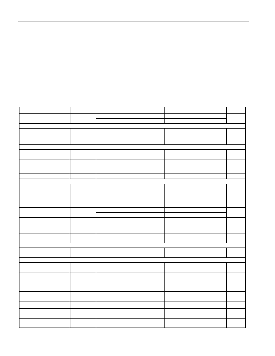
ELECTRICAL CHARACTERISTICS
(TPWR = 3.3V, T
A
= 0�C to +70�C, unless otherwise noted.)
PARAMETER SYMBOL
CONDITIONS
MIN
TYP
MAX
UNITS
LVD
2.7 5.5
TPWR Operating Supply
Range
V
TPWR
SE
4.0 5.5
V
TPWR SUPPLY CURRENT
I
TPWR_LVD
LVD SCSI mode
20
32
mA
I
TPWR_SE
SE SCSI mode
1.6
10
mA
TPWR Supply Current
(All Lines Open)
I
TPWR_ISO
ISO mode (terminators disabled)
250
750
mA
LVD TERMINATION (Applies to each line pair, 1 to 15 in LVD mode)
Differential-Mode
Termination Resistance
R
DM
100
110
W
Common-Mode
Termination Resistance
R
CM
R
P
and R
N
shorted together
110
165
W
Differential-Mode Bias
V
DM
All lines open
100
125
mV
Common-Mode Bias
V
CM
R
P
and R
N
shorted together
1.15
1.25
1.35
V
SE TERMINATION (Applies to SE terminators, 1 to 15 in SE mode)
Single-Ended Mode
Termination Resistance
R
SE
R
SE
= (V
Lx
- 0.2) / I
Lx
,
where V
Lx
= voltage at terminator
pin with pin unloaded and
I
Lx
= current for each terminator pin
with the pin forced to 0.2V (Note 2)
104.5 110 115.5
W
Signal level at 0.2V, all lines low
-21.0
-24
-25.4
Termination Current
(Note 2)
I
SE
Signal level at 0.5V
-18.0
-22.4
mA
SE Voltage Reference
V
REF
(Note
2)
2.7 2.85 3.0 V
Pin Leakage
With ISO high
400
nA
Single-Ended GND
Resistance
R
GND
Measured at R
P
pins, I = 10mA
20
60
W
TERMINATOR PIN CAPACITANCE
Terminator Pin
Capacitance
C
IN
With ISO high (Note 1)
3
pF
V
REF
REGULATOR
1.25V Regulator Output
Voltage
V
REF_LVD
1.15
1.25 1.35
V
1.25V Regulator Short-
Circuit Source Current
I
SOURCE
V
REF
= 0V
-375
-700
-1000
mA
1.25V Regulator Short-
Circuit Sink Current
I
SINK
V
REF
= 3.3V
170
300
700
mA
1.25V Regulator Line
Regulation
V
REF
unloaded; vary TPWR from
2.7V to 5.5V
1.0
2.5
%
2.85V Regulator
(Note 2)
2.7
2.85
3.0
V
2.85V Regulator Short-
Circuit Source Current
V
REF
= 0V (Note 2)
-375
-700
-1000
mA
2.85V Regulator Short-
Circuit Sink Current
V
REF
= 3.3V (Note 2)
170
300
700
mA

DS2125 Ultra3 LVD/SE SCSI 15-Line Terminator
3 of 7
ELECTRICAL CHARACTERISTICS (continued)
(TPWR = 3.3V, T
A
= 0�C to +70�C, unless otherwise noted.)
PARAMETER SYMBOL
CONDITIONS
MIN
TYP
MAX
UNITS
V
REF
REGULATOR
2.85V Regulator Line
Regulation
V
REF
unloaded; vary TPWR from
4.0V to 5.5V
1.0
2.5
%
DIFFSENS OUTPUT
DIFFSENS Driver Output
Voltage
V
DSO
-5mA
� I
DFFSENS
� 50mA
1.2 1.4
V
DIFFSENS Driver Source
Current
I
DSH
V
DIFFSENS
= 0V
-15
-5
mA
DIFFSENS Driver Sink
Current
I
DSL
V
DIFFSENS
= 3.3V
100
200
mA
I
LEAK, LOW
With ISO high, |V
DIFFSENS
| = 0.3V
-3
+1
DIFFSENS Leakage
(Note 3)
I
LEAK, HIGH
With ISO high, |V
DIFFSENS
- V
TPWR
| =
0.3V
1 3
mA
THERMAL SHUTDOWN
Thermal-Shutdown
Threshold
For increasing temperature
(Note 1)
150
�C
Thermal-Shutdown
Hysteresis
(Note
1)
10
�C
MODE CHANGE DELAY/FILTER
Mode Change Delay
t
DELAY
0.66 1.25 2.00 ms
LOGICAL SIGNALS (ISO)
Input Low Voltage
V
IL
-0.3
+0.8 V
Input High Voltage
V
IH
2
TPWR
+ 0.3
V
Input Current
I
IL
V
CC
= 3.3V
-30
-10
mA
DIFF_CAP
Input Current
I
L
V
IL
= -0.3V
-1
+1
mA
DIFF_CAP SE
Operating Range
V
SEOR
-0.3
+0.5 V
DIFF_CAP LVD
Operating Range
V
LVDOR
0.7
1.9
V
DIFF_CAP HVD
Operating Range
V
HVDOR
2.4
V
TPWR
+
0.3
V
Note 1: Guaranteed by design.
Note 2: TPWR = 4.0V.
Note 3: Room temperature only.
PIN DESCRIPTION
PIN NAME
FUNCTION
1, 2, 11�26,
37�48
RxP, RxN
Signal Termination. Connect to SCSI bus signal lines.
3 TPWR
Termination Power. Connect to the SCSI TERMPWR line and decouple with a 2.2
mF
capacitor.
4�9, 28�33
HS_GND
Heat-Sink Ground. Internally connected to the mounting pad. This should be grounded.
10 V
REF
Reference Voltage. 2.85V reference in SE mode and 1.25V reference in LVD mode; must be
decoupled with a 4.7
mF capacitor.
27
GND
Ground. Signal ground, 0V.
34 DIFF_CAP
DIFFSENSE Capacitor. Connect a 0.1
mF capacitor for the DIFFSENSE filter. Input to detect
the type of device (differential or single-ended) on the SCSI bus.
35
DIFFSENSE DIFFSENSE. Output to drive the SCSI bus DIFFSENS line.
36
ISO
Isolation. When pulled high, the DS2125 isolates its bus pins (RxN, RxP) from the SCSI bus.

DS2125 Ultra3 LVD/SE SCSI 15-Line Terminator
4 of 7
Figure 1. Block Diagram
R1N
R15P
R15N
R1P
Dallas
Semiconductor
DS2125
ISO
DIFFSENSE
DIFF_CAP
V
REF
THERMAL-
SHUTDOWN
CIRCUITRY
CONTROL
LOGIC
DIFFENSE
CIRCUITRY
BANDGAP
1.25V
10
W
10
W
V
REF
SE
LVD
HVD
SE GND
DRIVER
+
-
+
-
+
-

DS2125 Ultra3 LVD/SE SCSI 15-Line Terminator
5 of 7
Figure 2. SCSI Bus Configuration
Note: The following terms are used throughout this data sheet:
DIFFSENS: Refers to the SCSI bus signal.
DIFFSENSE: Refers to the DS2125 pin name and internal circuitry capable of driving the DIFFSENS line.
DIFF_CAP: Refers to the DS2125 pin name and internal circuitry relating to monitoring the DIFFSENS line.
DETAILED DESCRIPTION
The DS2125 combines LVD and SE termination with DIFFSENSE sourcing and detection. A bandgap reference is
fed into two amplifiers, which creates a 1.25V reference voltage and a 2.85V reference voltage. The control logic
determines which of these references are applied to the termination resistors. If the SCSI bus is in LVD mode, the
1.25V reference is used. If the SCSI bus is in SE mode, the 2.85V reference is used. That same control logic
switches in/out parallel resistors to change the total termination resistance accordingly. Finally, in SE mode the R
p
pins are switched to ground.
The DIFFSENSE circuitry decodes trinary logic. There is one of three voltages on the SCSI control line called
DIFFSENS. Two comparators and a NAND gate determine if the voltage is below 0.6V, above 2.15V, or in
between, which indicates the mode of the bus as SE, HVD, or LVD, respectively.
TERMPWR
TERMPWR
4.7
mF
0.1
mF
DIFFSENSE
TPWR
ISO
V
REF
DIFF_CAP
DIFFSENS
4.7
mF
TPWR
ISO
V
REF
DIFF_CAP
DIFFSENS
CONTROL LINES (15)
0.1
mF
TPWR
ISO
V
REF
DIFF_CAP
DIFFSENS
4.7
mF
4.7
mF
TPWR
ISO
V
REF
DIFF_CAP
DIFFSENS
CONTROL LINES (15)
20k
W
20k
W