DETAILED DESCRIPTION
1 of 32
REV: 012003
Note: Some revisions of this device may incorporate deviations from published specifications known as errata. Multiple revisions of any device
may be simultaneously available through various sales channels. For information about device errata, click here:
www.maxim-ic.com/errata
.
GENERAL DESCRIPTION
The DS2149 is a fully integrated LIU for long-
haul or short-haul T1 applications over twisted-
pair installations. It interfaces to two twisted-pair
lines--one pair for transmit and one pair for
receive through an appropriate network
interface. The device can be configured for
control through software or hardware mode.
Software control is accomplished over a serial
port, in hardware mode; individual pin settings
allow standalone operation. The device provides
a precise, crystal-less jitter attenuator that can be
placed in either the transmit or receive path.
APPLICATIONS
Routers
Data Service Units (DSUs)
Channel Service Units (CSUs)
Muxes
Switches
Channel Banks
T1/E1 Test Equipment
PIN CONFIGURATION
FEATURES
� Fully Integrated Line Interface Unit (LIU)
� Pin Compatible with LevelOne LXT362
� Supports Both Long Haul and Short Haul
� Crystal-Less Jitter Attenuator
� Jitter Attenuator Programmable for Transmit
or Receive Path
� Meets ANSI T1.102, T1.403, T1.408, and
AT&T 62411
� Usable Receive Sensitivity of 0dB to -36dB
That Allows the Device to Operate on
0.63mm (22AWG) Cables Up to 6k Feet in
Length
� Five Line Build-Out Settings for Short-Haul
Applications
� Four CSU Filters from 0dB to -22.5dB
� Transmit/Receive Performance Monitors
with Driver-Fail, Monitor-Open, and Loss-
of-Signal Outputs
� Bipolar or NRZ Interface
� Programmable B8ZS Encoder/Decoder
� QRSS Generator/Detector
� Local, Remote, and Analog Loopbacks
� Generates and Detects In-Band Loop-Up and
Loop-Down Codes
� Serial Interface Provides Access to Control
Registers
ORDERING INFORMATION
PART TEMP
RANGE
PIN-PACKAGE
DS2149Q
0�C to +70�C
28 PLCC
DS2149QN
-40�C to +85�C
28 PLCC
5
6
7
8
9
10
11
25
24
23
22
21
20
19
12
13
14
15
16
17
18
4
3
2
1
28
27
26
DS2149
TOP VIEW
PLCC
www.maxim-ic.com
DS2149
5V T1/J1 Line Interface Unit
DEMO KIT AVAILABLE

DS2149
2 of 32
TABLE OF CONTENTS
1.
DETAILED DESCRIPTION................................................................................................. 4
2.
OPERATING MODES......................................................................................................... 5
3.
INITIALIZATION AND RESET............................................................................................ 9
4.
REGISTER DEFINITIONS .................................................................................................. 9
5.
TRANSMITTER................................................................................................................... 15
5.1 T
RANSMIT
D
IGITAL
D
ATA
I
NTERFACE
................................................................................... 15
5.2 T
RANSMIT
M
ONITORING
...................................................................................................... 15
5.3 T
RANSMIT
I
DLE
M
ODE
......................................................................................................... 15
5.4 T
RANSMIT
P
ULSE
S
HAPE
.................................................................................................... 15
6.
RECEIVER.......................................................................................................................... 15
6.1 R
ECEIVE
E
QUALIZER
.......................................................................................................... 15
6.2 R
ECEIVE
D
ATA
R
ECOVERY
.................................................................................................. 15
6.3 R
ECEIVE
D
IGITAL
-D
ATA
I
NTERFACE
..................................................................................... 16
6.4 R
ECEIVE
M
ONITOR
M
ODE
................................................................................................... 16
7.
JITTER ATTENUATION ..................................................................................................... 16
8.
HARDWARE MODE ........................................................................................................... 16
9.
SOFTWARE MODE ............................................................................................................ 17
9.1 I
NTERRUPT
H
ANDLING
........................................................................................................ 17
10.
DIAGNOSTIC MODE OPERATION.................................................................................... 19
10.1 L
OOPBACK
M
ODES
............................................................................................................. 20
10.1.1
Local Loopback (LLB).................................................................................................................20
10.1.2
Analog Loopback (ALB)..............................................................................................................20
10.1.3
Remote Loopback (RLB) ............................................................................................................20
10.1.4
Network Loopback......................................................................................................................20
10.1.5
Dual Loopback ...........................................................................................................................20
10.2 I
NTERNAL
P
ATTERN
G
ENERATION AND
D
ETECTION
............................................................... 21
10.2.1
Transmit Alarm-Indication Signal (TAIS).....................................................................................21
10.2.2
Quasirandom Signal Source (QRSS) .........................................................................................21
10.2.3
In-Band Network Loop-Up or Loop-Down Code Generator.........................................................22
10.3 E
RROR
I
NSERTION AND
D
ETECTION
..................................................................................... 22
10.3.1
Bipolar Violation Insertion (INSBPV)...........................................................................................22
10.3.2
Logic Error Insertion (INSLE)......................................................................................................22
10.3.3
Logic Error Detection (QPD).......................................................................................................22
10.3.4
Bipolar Violation Detection (BPV) ...............................................................................................22
10.4 A
LARM
M
ONITORING
........................................................................................................... 23
10.4.1
Receive-Carrier Loss (RCL) .......................................................................................................23
10.4.2
Alarm-Indication-Signal Detection (AIS)......................................................................................23
10.4.3
Driver-Fail Monitor-Open (DFMO) ..............................................................................................23
10.4.4
Jitter Attenuator Limit Trip (JALT) ...............................................................................................23
10.5 O
THER
D
IAGNOSTIC
R
EPORTS
............................................................................................ 23
10.5.1
Receive Line-Attenuation Indication ...........................................................................................23
11.
NETWORK INTERFACE .................................................................................................... 24
12.
DC CHARACTERISTICS.................................................................................................... 28
13.
PACKAGE INFORMATION ................................................................................................ 32

DS2149
3 of 32
LIST OF FIGURES
Figure 1-1. Block Diagram....................................................................................................................................... 4
Figure 2-1. Hardware Mode Pinout ........................................................................................................................ 6
Figure 2-2. Serial Port Mode Pinout....................................................................................................................... 6
Figure 9-1. Serial Data Port Operation for Read Access.................................................................................. 18
Figure 9-2. Serial Data Port Operation for Write Access.................................................................................. 18
Figure 10-1. Loopbacks in the DS2149 Block Diagram.................................................................................... 21
Figure 11-1. Basic Network Interface .................................................................................................................. 25
Figure 11-2. T1 Transmit Pulse Template .......................................................................................................... 26
Figure 11-3. Jitter Tolerance ................................................................................................................................. 27
Figure 11-4. Jitter Attenuation............................................................................................................................... 27
Figure 12-1. Serial Bus Read Timing (MODE1 = 1) .......................................................................................... 29
Figure 12-2. Serial Bus Write Timing (MODE1 = 1) .......................................................................................... 29
Figure 12-3. AC Characteristics for Receive Side ............................................................................................. 30
Figure 12-4. AC Characteristics for Transmit Side ............................................................................................ 31
LIST OF TABLES
Table 2-A. Operating Modes ................................................................................................................................... 5
Table 2-B. Control Pins for Hardware and Software Modes .............................................................................. 5
Table 2-C. Signal Descriptions ............................................................................................................................... 7
Table 4-A. Register Map.......................................................................................................................................... 9
Table 4-B. Register Bit Positions............................................................................................................................ 9
Table 4-C. Jitter Attenuator Selection.................................................................................................................. 10
Table 4-D. Line Code and Interface Selection ................................................................................................... 10
Table 4-E. Line Build-out Selection...................................................................................................................... 10
Table 4-F. Data Pattern Selection ........................................................................................................................ 11
Table 9-A. CLKE Pin Selection............................................................................................................................. 17
Table 9-B. Control and Operation Mode Selection............................................................................................ 19
Table 10-A. Diagnostic Modes.............................................................................................................................. 19
Table 11-A. Specifications for Receive Transformer......................................................................................... 24
Table 11-B. Specifications for Transmit Transformer........................................................................................ 24
Table 11-C. Transformer Turns Ratio vs. Series Resistance .......................................................................... 24
DS2149
4 of 32
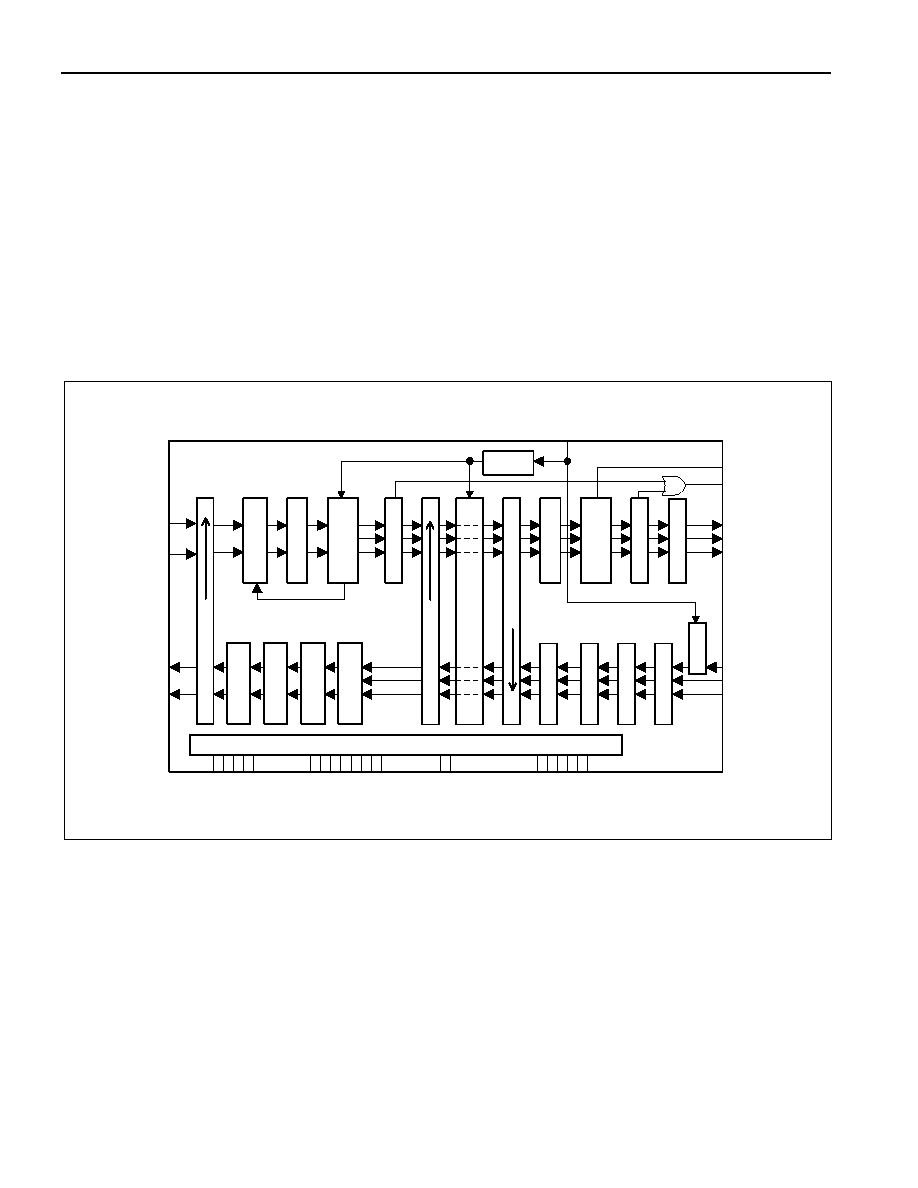
1. DETAILED DESCRIPTION
The DS2149 is a complete T1 line interface unit (LIU) for short-haul and long-haul applications. Receive
sensitivity adjusts automatically to the incoming signal and can be limited to -18dB, -26dB, or
-36dB. The device can generate the necessary DSX-1 line build-outs or CSU line build-outs of 0dB,
-7.5dB, -15dB, and -22.5dB. The on-board crystal-less jitter attenuator requires a 1.544MHz reference
clock. The jitter attenuator FIFO is selectable to either 32 bits or 128 bits in depth and can be placed in
either the transmit or receive data paths. The DS2149 has diagnostic capabilities such as loopbacks and
QRSS pattern generation and detection. The device can also generate and detect the in-band loop-up and
loop-down codes specified in AT&T 62411. The device can be configured for control using a serial
interface, or for hardware mode. The device fully meets all of the latest T1 specifications including ANSI
T1.102-1999, ANSI T1.403-1999, ANSI T1.408, and AT&T 62411.
Figure 1-1. Block Diagram
L
o
c
a
l
L
o
o
p
b
a
c
k
R
e
m
o
t
e
L
o
o
p
b
a
c
k
A
n
a
l
o
g
L
o
o
p
b
a
c
k
J
i
tter
A
ttenuator
TRING
TTIP
RRING
RTIP
L
i
n
e
D
r
i
v
e
r
s
C
S
U
F
i
l
t
e
r
s
W
a
v
e
S
h
a
p
i
n
g
F
i
l
t
e
r
P
e
a
k
D
e
t
e
c
t
C
l
o
c
k
/
D
a
t
a
R
e
c
o
v
e
r
y
B
8
Z
S
E
n
c
o
d
e
r
L
o
g
i
c
E
r
r
o
r
I
n
s
e
r
t
TPOS
TCLK
TNEG
Q
R
S
S
I
n
B
a
n
d
L
o
o
p
g
e
n
.
B
8
Z
S
D
e
c
o
d
e
r
I
n
B
a
n
d
L
o
o
p
C
o
d
e
D
e
t
e
c
t
o
r
Q
R
S
S
D
e
t
e
c
t
o
r
RPOS
RCLK
RNEG
M
C
L
K
R
C
L
D
e
t
e
c
t
o
r
RCL/QPD
NLOOP
MO
D
E
0
MO
D
E
1
Power connections Hardware Interface Serial Interface
INT
CL
K
E
SC
L
K
SD
I
SD
O
CS
J
ASE
L
L0
L1
L2
L3
LLB
RL
B
TB
L
/
Q
R
S
S
VS
M
TV
D
D
VD
D
GN
D
GN
D
T
r
n
a
s
m
i
t
A
I
S
A
I
S
d
e
t
e
c
t
L
O
T
C
m
u
x
VCO / PLL

DS2149
5 of 32
2. OPERATING MODES
The DS2149 has several pins with multiple functions and names according to the selected operating
mode. These operating modes are summarized in the tables below.
Table 2-A. Operating Modes
QRSS DISABLED
QRSS ENABLED
PIN
BIPOLAR NRZ BIPOLAR NRZ
1 MCLK
2 TCLK
3 TPOS TDATA
INSLER
4 TNEG INSBPV
INSBPV
6 RNEG BPV RNEG BPV
7 RPOS RDATA RPOS RDATA
8 RCLK
13 TTIP
16 TRING
19 RTIP
20 RRING
Control pins are affected by serial port and hardware modes.
Table 2-B. Control Pins for Hardware and Software Modes
HARDWARE MODE
SERIAL PORT MODE
PIN
NRZ QRSS NRZ QRSS
5 MODE1
MODE1
9 MODE0
MODE0
11 JASEL
N.C.
12 RCL RCL/QPD RCL RCL/QPD
23 L0
INT
24 L1
SDI
25 L2
SDO
17 L3
N.C.
18 NLOOP
NLOOP
26 RLB NLB
CS
27 LLB ALB
SCLK
28 TAIS QRSS
CLKE
Document Outline