 | ÐлекÑÑоннÑй компоненÑ: DS2156DK | СкаÑаÑÑ:  PDF PDF  ZIP ZIP |
COMPONENT LIST
1 of 21
REV: 060303
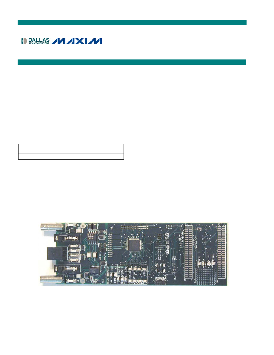
GENERAL DESCRIPTION
The DS2155/DS2156 design kits are evaluation
boards for the DS2155 and DS2156. The
DS2155/DS2156 design kits are intended to be used
as daughter cards with either the DK2000 or the
DK101 motherboards. The boards are complete with
a single-chip transceiver (SCT), transformers,
termination resistors, configuration switches, line
protection circuitry, network connectors, and an
interface to the motherboard.
ORDERING INFORMATION
PART DESCRIPTION
DS2155DK
DS2155 Design Kit Daughter Card
DS2156DK
DS2156 Design Kit Daughter Card
FEATURES
§
Expedites New Designs by Eliminating First-Pass
Prototyping
§
Interfaces Directly to the DK101 or DK2000
Motherboards
§
Demonstrates Key Functions of the DS2156 and
DS2155
§
High-Level Software Provides Visual Access to
Registers
§
Software-Controlled (Register Mapped)
Configuration Switches to Facilitate Clock and
Signal Routing
§
BNC Connections for 75
W E1
§
Bantam and RJ48 Connectors for 120
W E1 and
100
W T1
§
Multitap Transformer to Facilitate True
Impedance Matching for 75
W and 120W/100W
Paths
§
Network Interface Protection for Overvoltage and
Overcurrent Events
§
UTOPIA II Bus Connection for MPC8260
(DS2156 Only)
§
UTOPIA II Prototype Connectors (DS2156 Only)
§
Test Points and Prototype Area Available for
Further Customization
DS2155DK/DS2156DK
T1/E1/J1 Single-Chip Transceiver
Design Kit Daughter Cards
www.maxim-ic.com

DS2155DK/DS2156DK T1/E1/J1 Single-Chip Transceiver Design Kit Daughter Cards
2 of 21
TABLE OF CONTENTS
COMPONENT LIST.....................................................................................................................3
BASIC OPERATION....................................................................................................................4
H
ARDWARE
C
ONFIGURATION
.................................................................................................................. 4
Q
UICK
S
ETUP
(D
EMO
M
ODE
) .................................................................................................................. 4
Q
UICK
S
ETUP
(R
EGISTER
V
IEW
) ............................................................................................................. 4
S
AMPLE
UTOPIA II C
ONFIGURATION
(DS2156 O
NLY
)............................................................................. 5
REGISTER MAP..........................................................................................................................5
CPLD R
EGISTER
M
AP
........................................................................................................................... 6
DS2155/DS2156 INFORMATION................................................................................................8
DS2155DK/DS2156DK INFORMATION......................................................................................8
TECHNICAL SUPPORT ..............................................................................................................8
SCHEMATICS .............................................................................................................................8
LIST OF TABLES
Table 1. Daughter Card Address Map .........................................................................................5
Table 2. CPLD Register Map .......................................................................................................6

DS2155DK/DS2156DK T1/E1/J1 Single-Chip Transceiver Design Kit Daughter Cards
3 of 21
COMPONENT LIST
DESIGNATION QTY
DESCRIPTION SUPPLIER
PART
C1C5, C8C12,
C15C19, C21,
C22, C29C34
23
0.1
mF 10%, 16V ceramic capacitors (0603)
Digi-Key 311-1088-1-ND
C7, C36
2
1
mF 10%, 16V ceramic capacitors (1206)
Digi-Key PCC1882CT-ND
C13, C14
2
0.1
mF 10%, 16V ceramic capacitors (0805)
Digi-Key 311-1142-1-ND
C23 1
0.1
mF 10%, 25V ceramic capacitor (1206)
Digi-Key PCC1883CT-ND
C24C27 4
0.22
mF, 50V ceramic capacitors
Digi-Key UNK
C35 1
10
mF 20%, 16V tantalum capacitor (B case)
Digi-Key PCS3106CT-ND
DS1, DS4DS18
16
LED, green, SMD
Digi-Key
P501CT-ND
DS2, DS3
2
LED, red, SMD
Digi-Key
P500CT-ND
F1F6
6
250V, 1.25A fuse, SMT
Teccor Electronics
F1250T
J1, J2
2
Male 0.1, SMD, 50-pin, dual-row vertical
Samtec
TSM-125-01-T-DV
J3, J4
2
Bantam connectors
SWK
RTT34B02
J5, J6
2
Connector BNC RA 5-pin
Kruvand
UCBJR220
J7J9
3
Socket, SMD, 50-pin, dual-row vertical
Samtec
TFM-125-02-S-D-
LC
JT10
1
Connector, 10-pin, dual-row vertical
Digi-Key
S2012-05-ND
L1 1
Choke, dual 4-line 24
mH, 8-pin SO
Pulse Engineering
PE-65857
R1, R14, R21
3
51.1
W 1%, 1/8W resistors (1206)
Digi-Key P51.1FCT-ND
R2, R3, R58, R59
4
0
W 5%, 1/8W resistors (1206)
Digi-Key P0.0ETR-ND
R4, R5, R60
3
51.1
W 1%, 1/10W resistors (0805)
Digi-Key P51.1CCT-ND
R6, R9, R10, R13,
R15R19, R22,
R23, R25R29,
R32, R37, R38,
R44, R47R49, R61
24
10k
W 1%, 1/10W resistors (0805)
Digi-Key P10.0KCCT-ND
R7, R8, R11, R12,
R30, R31, R35,
R36, R39R43,
R45, R50R53
18
330
W 0.1%, 1/10W MF resistors (0805)
Digi-Key P330ZCT-ND
R24 1
1.0k
W 1%, 1/10W resistor (0805)
Digi-Key P1.00KCCT-ND
R33, R34
2
NOPOP
--
NOPOP
R46 1
4.7k
W 1%, 1/8W resistor (0805)
Digi-Key
9C08052A4701FK
HFT
R54, R55
2
61.9
W 1%, 1/8W resistors (1206)
Digi-Key P61.9FCT-ND
R56, R57
2
49.9
W 1%, 1/8W resistors (1206)
Digi-Key P49.9FCT-ND
RJ1 1
RJ48
connector
Molex
43223
SW1
1
Switch DPDT slide 6-pin TH
Avnet
SSA22
T1
1
XFMR 16-pin SMT
Pulse Engineering
TX1099
U11
1
T1/E1/J1 XCVR 100-pin QFP, 0°C to +70°C
Dallas Semiconductor
DS2156L
U1U4, U6
5
BBUS switch 10-bit CMOS, 150-mil, 24-pin SO IDT
IDTQS3R861Q
U5
1
144-pin macrocell CPLD
Avnet
XC95144XL-
10TQ100C
U7U10
4
Quad bus switch, 150-mil, 16-pin SO
IDT
IDTQS3125Q
Z1, Z6Z8
4
160V, 500A Sidactor
Teccor Electronics
P1800SCMC
Z2, Z3
2
58V, 500A Sidactor
Teccor Electronics
P0640SCMC
Z4, Z5
2
6V, 50A Sidactor
Teccor Electronics
P0080SAMC
Z9, Z10
2
25V, 500A Sidactor
Teccor Electronics
P0300SCMC

DS2155DK/DS2156DK T1/E1/J1 Single-Chip Transceiver Design Kit Daughter Cards
4 of 21
BASIC OPERATION
This design kit relies upon several supporting files, which can be downloaded from our website at
www.maxim-
ic.com/DS2155DK
.
Hardware Configuration
Using the DK101 processor board:
· Connect the daughter card to the DK101 processor board.
· Supply 3.3V to the banana-plug receptacles marked GND and VCC_3.3V. (The external 5V connector and the
TIM 5V supply headers are unused.)
· All processor board DIP switch settings should be in the ON position with exception for the flash programming
switch, which should be OFF.
· From the Programs menu launch the host application named ChipView.exe. Run the ChipView application. If
the default installation options were used, click the Start button on the Windows toolbar and select
Programs
®ChipView®ChipView.
Using the DK2000 processor board:
· Connect the daughter card to the DK2000 processor board.
· Connect J1 to the power supply that is delivered with the kit. Alternately, a PC power supply can be connected
to connector J2.
· From the Programs menu launch the host application named ChipView.exe. Run the ChipView application. If
the default installation options were used, click the Start button on the Windows toolbar and select
Programs
®ChipView®ChipView.
General:
· Upon power-up the RLOS LED is lit, as well as the MCLK-2.048MHz and TCLK-2.048MHz LEDs.
· Due to the dual winding transformer, only the 120W line build-out configuration setting is needed to cover 75W
E1 and 120
W E1.
Quick Setup (Demo Mode)
· The PC loads the program, offering a choice among Demo Mode, Register View, and Terminal Mode. Select
Demo Mode.
· The program requests a configuration file, then select between the displayed files.
(DS2155_E1_DSNCOM_DRVR.cfg or DS2155_T1_DSNCOM_DRVR.cfg).
· The Demo Mode screen appears. Upon external loopback, the LOS and OOF indicators extinguish.
Quick Setup (Register View)
· The PC loads the program, offering a choice among Demo Mode, Register View, and Terminal Mode. Select
Register View.
· The program requests a definition file, then select DS2155.def.
· The Register View screen appears, showing the register names, acronyms, and values.
· Predefined register settings for several functions are available as initialization files.
¾ INI files are loaded by selecting the menu File®Reg Ini File®Load Ini File.
¾ Load the INI file DS2155_T1_BERT_ESF.ini.
¾ After loading the INI file the following may be observed:
The RLOS LED extinguishes upon external loopback.
The DS2155/DS2156 begins transmitting a Daly pattern. When external loopback is applied, the BERT
bit-count registers BBC13 and BEC13 may be updated by clearing and setting BC1.LC and
clicking the Read All button.
Miscellaneous:
· Clock frequencies and certain pin bias levels are provided by a register-mapped CPLD, which is on the
DS2155/DS2156 daughter card.
· The definition file for this CPLD is named DS215x_35x_CPLD_V2.def. See the
CPLD Register Map
section for
definitions.
· All files referenced above are available for download at
www.maxim-ic.com/DS2155DK
.
DS2155DK/DS2156DK T1/E1/J1 Single-Chip Transceiver Design Kit Daughter Cards
5 of 21
Sample UTOPIA II Configuration (DS2156 Only)
The following register settings configure the DS2156 daughter card for UTOPIA II, single CLAV, 8-bit mode on PHY
port 0. UTOPIA II bus connection is provided by header J1 (Tx) and header J2 (Rx).
After configuring the following registers toggle the MSTREG.URST bit to reset the UTOPIA II core.
UTOPIA II Setup, Register Settings for daughter card CPLD
NAME VALUE
NAME
VALUE
SWITCH 1
0x0F
SWITCH 4
0x0F
SWITCH 2
0x03
LEVELS
0x07
SWITCH 3
0x0F
UTOPIA II Setup, Register Settings for DS2156 E1 Configuration
NAME VALUE
NAME
VALUE
MSTREG 0x02
LBCR 0x00
E1RCR1 0x68
TAF 0x9B
E1RCR2 0x00
TNAF 0xC0
E1TCR1 0x15
LIC1 0x11
E1TCR2 0x00
LIC2 0x90
CCR1 0x00
LIC3 0x00
CCR4 0x00
LIC4 0x00
IOCR1 0x00
IOCR2 0x00
UTOPIA II Setup, Register Settings for DS2156 UTOPIA II Configuration
NAME VALUE
NAME
VALUE
U_TCFR 0x01
U_RCR2 0x0
U_TCR1 0x05
U_TIUPB 0x0
U_TCR2 0x00
PCPR 0x22
U_RCFR
0x01
PCDR1, 2, 3, 4
0x0
U_RCR1 0x01
REGISTER MAP
The DK101 daughter card address space begins at 0x81000000.
The DK2000 daughter card address space begins at:
0x30000000 for slot 0
0x40000000 for slot 1
0x50000000 for slot 2
0x60000000 for slot 3
All offsets given in
Table 1
are relative to the beginning of the daughter card address space.
Table 1. Daughter Card Address Map
OFFSET DEVICE
DESCRIPTION
0X0000
to
0X0015
CPLD
Board identification and clock/signal routing
0X1000
to 0X10ff
Single-Chip
Transceiver
Board is populated with one of the following:
DS2156, DS2155, DS21352, or DS21354.
Please see data sheet for details.
Registers in the CPLD can be easily modified using the ChipView.exe, a host-based user interface software along
with the definition file named DS215x_35x_CPLD_V2.def. Definition files for the SCT are named DS2155.def,
DS21352.def, or DS21354.def, depending on the board population option.
Document Outline