 | ÐлекÑÑоннÑй компоненÑ: DS2174DK | СкаÑаÑÑ:  PDF PDF  ZIP ZIP |
/home/web/htmldatasheet/html/maxim/170444
1 of 12
REV: 052103
GENERAL DESCRIPTION
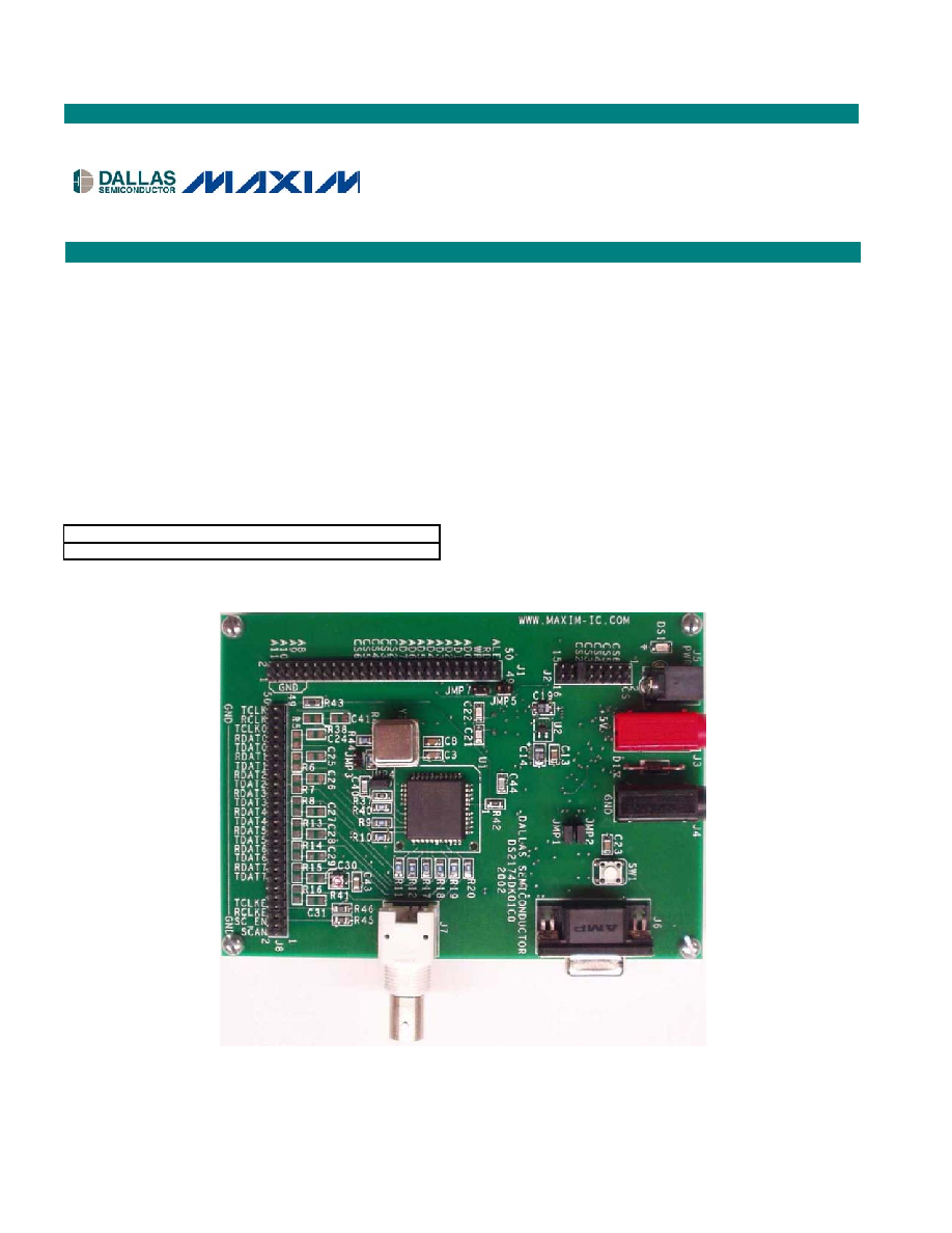
The DS2174DK is a fully integrated demonstration kit
for the DS2174 enhanced bit error-rate tester
(BERT). This demo kit contains all the necessary
circuitry to evaluate the device in all modes of
operation. The boards are complete with a DS2174,
on-board microcontroller with RS-232 control, test
points for all IO pins on the BERT, and an
address/data header for connection to an external
prototyping system.
ORDERING INFORMATION
PART DESCRIPTION
DS2174DK
BERT Design Kit
FEATURES
§ A Soldered DS2174 in the 44-Pin PLCC Package
for Maximum Signal Integrity
§ On-Board Selectable Oscillator for TCLK
§ On-Board Selectable Analog Input for TCLK
§ On-Board 8051 Microprocessor for Software
Mode Access
§ Selectable CS for the DS2174; Used for Either
Multiboard Operation or System Level
Development
§ Signal Termination on all High-Speed Transmit
and Receive Paths
DS2174DK
Enhanced Bit Error-Rate Tester
Design Kit
www.maxim-ic.com
DS2174 Design Kit
2 of 12
COMPONENT LIST
DESIGNATION QTY
DESCRIPTION SUPPLIER
PART
C1, C2, C23
3
1
mF 10%, 16V ceramic capacitors (1206)
Panasonic ECJ-3YB1C105K
C3C7, C13,
C43, C45C48
11
0.1
mF 10%, 25V ceramic capacitors (1206)
Panasonic ECJ-3VB1E104K
C8C12 5
0.01
mF 10%, 50V ceramic capacitors (1206)
Panasonic ECU-V1H103KBM
C14, C16C20
6
10
mF 20%, 16V tantalum capacitors (B case)
Panasonic ECS-T1CX106R
C15 1
68
mF 20%, 16V tantalum capacitor (D case)
Panasonic ECS-T1CD686R
C21, C22
2
22pF 10%, 100V ceramic capacitors (1206)
AVX
12061A220KAT2A
C24C31, C41
9
Do not place ceramic capacitors (1206)
--
--
C32C40, C44
10
56pF 5%, 50V tall case ceramic capacitors (1206)
Phycomp
1206CG560J9B200
C42 1
0.001
mF 10%, 50V ceramic capacitor (1206)
Panasonic ECU-V1H102KBM
D1
1
1A, 50V general-purpose silicon diode
Vishay (formerly General
Semiconductor)
1N4001
DS1
1
LED, red, SMD
Panasonic
LN1251C
J1
1
50-pin connector, dual row
Samtec
SSW-125-01-T-D
J2
1
16-pin header, dual row vertical
Samtec
HDR-TSW-18-14-T-D
J5
1
3-pin header, receptacle jack, right angle
Samtec
RAPC712
J6
1
DB9 connector, short case, right angle
AMP
788750-2
J7 1
BNC 50
W PC board bulkhead jack, right angle
Amphenol 31-5431
J8
1
Socket strip, 50-pin header, dual row vertical
Samtec
SSW-125-01-T-D
JMP1JMP5,
JMP7
6
Jumpers, 2-pin headers (100 mil)
AMP
R1 1
330
W 1%, 1/8W resistor (1206)
Panasonic ERJ-8ENF3300V
R2, R3, R45,
R46
4
10k
W 1%, 1/8W resistors (1206)
Panasonic ERJ-8ENF1002V
R4, R9R12,
R17R20, R40,
R44, R47
12
30.1
W 1%, 1/8W resistors (1206)
Panasonic ERJ-8ENF30R1V
R5R8,
R13R16, R38
9
Do not place resistors (1206)
--
--
R21R24,
R29R32, R37,
R39, R42
11
100
W 1%, 1/8W resistors (1206)
Panasonic ERJ-8ENF1000V
R25R28,
R33R36, R43
9
0
W 5%, 1/8W resistors (1206)
Panasonic ERJ-8GEYJ0R00V
R41 1
10k
W 0.05W, 15V variable 1-turn resistor
Panasonic EVM-7JSX30B14
SW1
1
4-pin, single-pole, light-touch switch
Panasonic
EVQPAE04M
U1
1
DS2174 EBERT (44-Pin TQFP, 0°C to +70°C)
Dallas Semiconductor
DS2174
U2
1
300mA, 3.3V, 5-pin SOT23 voltage regulator
Maxim
MAX8887EZK33
U3, U7, U8
3
Latch octal D-type with 5V inputs, 20-pin TSSOP
Texas Instruments
SN74LCX373PWR
U4
1
Dual RS-232 transmitter/receiver (150-mil 16-pin SO) Dallas Semiconductor
DS232AR
U5
1
DS87C520-ECL high-speed microcontroller
Dallas Semiconductor
DS87C520-ECL
U6
1
3-to-8 line decoder (16-pin SO)
Toshiba
TC74HC138AFN
U9
1
Quad line receiver (16-pin SO)
Maxim
MAX9126ESE
Y1
1
11.0592MHz low-profile crystal
Dove Electronics
EC1-S-11.0592M
Y2
1
Half-size socket (8-pin STD DIP)
Aries Electronics
1108800
DS2174 Design Kit
3 of 12
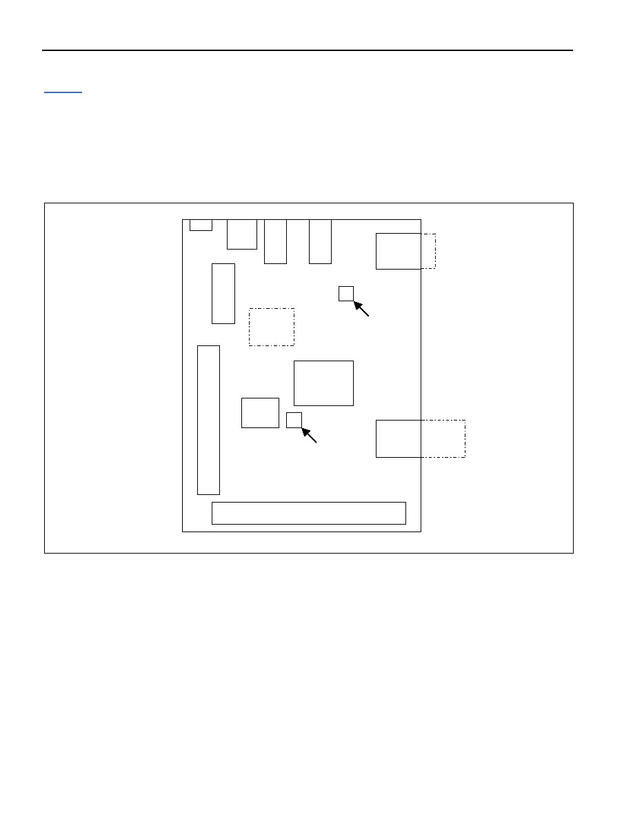
BOARD FLOORPLAN
Figure 1
shows the board layout for the DS2174DK. The DS2174 PLCC device is in the center of the board. All the
power connectors can be found on the top of the design kit. This includes the two banana jack connectors and the
three terminal connectors for a 5V DC power supply. The RS-232 serial connector and the BNC connector for the
TCLK analog input are along the right side of the board. The chip-select header and address/data bus header are
on the left-hand side. The system connector with all the telecom I/O signals is at the bottom of the board. The
microcontroller is on the bottom side of the board, slightly above the DS2174. Please notice in Figure 1 the dashed
outline indicating the location of assembly. Please look in the general locations on the board when this document
references specific items on the DS2174DK.
Figure 1. Board Floorplan
SYSTEM CONNECTOR
DS2174
OSC
VD
D
GND
PWR
LED
SERIAL
PORT
mC
5V
RE
G
CS6
CS5
CS4
CS3
CS2
CS
ANALOG
OSC
A
DDRESS
/
D
AT
A
B
U
S
mC CONTROL
JMP1, JMP2
TCLK
CONTROL
JMP3, JMP4
DS2174 Design Kit
4 of 12
SYSTEM CONNECTOR
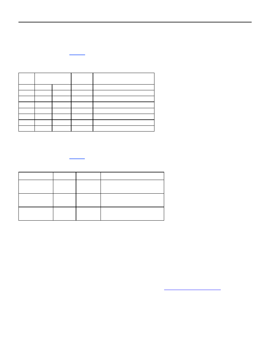
A 50-pin system connector (J8) at the bottom of the board gives access to the following DS2174 signals: TCLK,
RCLK, TCLKO, RDAT0RDAT7, TDAT0TDAT7, TCLKE, RCLKE, SC_E (SCAN ENABLE), and SCAN. By using
jumpers to connect TCLK to RCLK, or RCLK to TCLKO, TDATX to RDATX, the system connector can also be used
to implement an external loopback for part development and verification. With this feature, you can quickly use this
design kit as a working prototype for your system.
Table 1
shows a representation of the system connector. Please
keep in mind signal names in relationship to the pin number on the connector. Due to the termination placement on
the telecom signals, the board's silkscreen was moved below the connector.
Table 1. System Connector (J8)
PIN NAME PIN
50 GND TCLK 49
48 GND RCLK 47
46 GND TCLKO 45
44 GND RDAT0 43
42 GND TDAT0 41
40 GND RDAT1 39
38 GND TDAT1 37
36 GND RDAT2 35
34 GND TDAT2 33
32 GND RDAT3 31
30 GND TDAT3 29
28 GND RDAT4 27
26 GND TDAT4 25
24 GND RDAT5 23
22 GND TDAT5 21
20 GND RDAT6 19
18 GND TDAT6 17
16 GND RDAT7 15
14 GND TDAT7 13
12 GND --
11
10 GND --
9
8 GND TCLKE 7
6 GND
RCLKE 5
4 GND SC_EN 3
2 GND SCAN 1
DS2174 Design Kit
5 of 12
DS2174DK MEMORY MAP
The DS2174DK can be configured to suit a variety of needs. For example, this demo kit can be used as a stand-
alone design kit or it may be configured together with two DS2174DKs. The board can also be used with another
system by using the on-board microcontroller or disabling the microcontroller and using the address/data bus
header that is provided.
Table 2
shows how you can determine the base memory location for the DS2174 on the
board.
Table 2. Pin Definitions of Chip Select Header (J2)
PIN NAME PIN
MEMORY ADDRESS WHEN
JUMPER IS IN PLACE
J2.1 -- -- J2.2
Not
Used
J2.3
CS6
CS
J2.4
6000h to 6FFFh
J2.5
CS5
CS
J2.6
5000h to 5FFFh
J2.7
CS4
CS
J2.8
4000h to 4FFFh
J2.9
CS3
CS
J2.10
3000h to 3FFFh
J2.11
CS2
CS
J2.12
00h to 2FFFh
J2.13 --
--
J2.14 Not
Used
J2.15 --
--
J2.16 Not
Used
DS2174DK TCLK SELECTION
The DS2174DK provides three separate sources for TCLK: an on-board crystal oscillator, analog input, or TCLK
from the system header.
Table 3
shows the different sources for TCLK and how to configure the DS2174DK.
Table 3. TCLK Selection
TCLK SOURCE
JMP3
JMP4
FUNCTION
OSC (Y2)
Open
Closed
RCLK can be wired to TCLK or
TCLKO on the system connector
Analog Input
Closed
Open
RCLK can be wired to TCLK or
TCLKO on the system connector
TCLK Open
Open
RCLK can be wired to TCLKO or
driven on the system connector
POWER-SUPPLY CONNECTORS
Connect a 5.0V power supply across the red (V
DD
) and black (GND) banana jacks. The red PWR LED indicates
power is applied to the board. A voltage regulator then drops the supply to 3.3V, which is supplied to the DS2174. If
you want to bring 5.0V and 3.0V to the address/data bus header, the JMP5 and JMP7 connectors should be
closed.
MICROCONTROLLER AND SERIAL CONNECTOR
The DS2174DK has an on-board 8051 microcontroller with factory-installed firmware loaded in the microcontroller's
EPROM. This firmware translates memory access requests from the RS-232 serial port (57.6kB) to the
address/data bus. Dallas Semiconductor has created a software application called ChipView that allows easy read-
write access for this device. Download the application from our website,
www.maxim-ic.com/telecom
.
Close JMP1 and JMP2 to enable the on-board microcontroller. If you are using an external controller to
communicate with the DS2174, JMP1 and JMP2 must remain open to tri-state the address/data bus.
If desired, the user can access the memory location on the board through any serial terminal program. All the write
and read commands are distinguished with an "X" followed by the memory location. Depending on if it is a write or
a read, the user provides data to be written to the memory location or expects data from the device.