1 of 87
REV: 013004
Note: Some revisions of this device may incorporate deviations from published specifications known as errata. Multiple revisions of any device
may be simultaneously available through various sales channels. For information about device errata, click here:
www.maxim-ic.com/errata
.
GENERAL DESCRIPTION
The DS21Q50 E1 quad transceiver contains all the
necessary functions for connecting to four E1 lines.
The on-board clock/data recovery circuitry coverts
the AMI/HDB3 E1 waveforms to an NRZ serial
stream. The DS21Q50 automatically adjusts to E1
22AWG (0.6mm) twisted-pair cables from 0km to
over 2km in length. The device can generate the
necessary G.703 waveshapes for both 75
W coax and
120
W twisted-pair cables. The on-board jitter
attenuators (selectable to either 32 bits or 128 bits)
can be placed in either the transmit or receive data
paths. The framers locate the frame and multiframe
boundaries and monitor the data streams for alarms.
The device contains a set of internal registers, from
which the user can access and control the operation
of the unit by the parallel control port or serial port.
The device fully meets all the latest E1 specifications
including ITU-T G.703, G.704, G.706, G.823, G.732,
and I.431 ETS 300 011, ETS 300 233, and ETS 300
166 as well as CTR12 and CTR4.
APPLICATIONS
DSLAMs
Routers
IMA and WAN Equipment
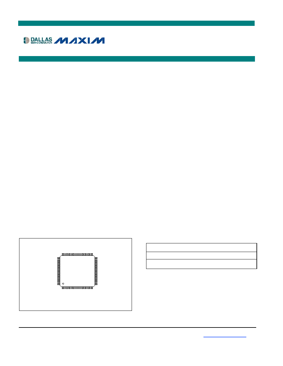
PIN CONFIGURATION
FEATURES
§
Four Complete E1 (CEPT) PCM-30/ISDN-PRI
Transceivers
§ Long-Haul and Short-Haul Line Interfaces
§ 32-Bit or 128-Bit Crystal-Less Jitter Attenuator
§ Frames to FAS, CAS, CCS, and CRC4 Formats
§ 4MHz/8MHz/16MHz Clock Synthesizer
§ Flexible System Clock with Automatic Source
Switching on Loss-of-Clock Source
§ Two-Frame Elastic-Store Slip Buffer on the
Receive Side
§ Interleaving PCM Bus Operation Up to
16.384MHz
§ Configurable Parallel and Serial Port Operation
§ Detects and Generates Remote and AIS Alarms
§ Fully Independent Transmit and Receive
Functionality
§ Four Separate Loopback Functions
§ PRBS Generation/Detection/Error Counting
§ 3.3V Low-Power CMOS
§ Large Counters for Bipolar and Code Violations,
CRC4 Codeword Errors, FAS Word Errors, and
E Bits
§ Eight Additional User-Configurable Output Pins
§
100-Pin, 14mm x 14mmLQFP Package
ORDERING INFORMATION
PART TEMP
RANGE
PIN-PACKAGE
DS21Q50L
0°C to +70°C
100 LQFP (14mm)
DS21Q50LN
-40°C to +85°C
100 LQFP (14mm)
DS21Q50
Quad E1 Transceiver
www.maxim-ic.com
1
100
LQFP
DS21Q50
TOP VIEW

DS21Q50
2 of 87
TABLE OF CONTENTS
1. INTRODUCTION ...............................................................................................................................6
2. PIN DESCRIPTION............................................................................................................................9
2.1 P
IN
F
UNCTION
D
ESCRIPTION
.........................................................................................................15
2.1.1
System (Backplane) Interface Pins .......................................................................................................15
2.1.2
Alternate Jitter Attenuator ....................................................................................................................16
2.1.3
Clock Synthesizer..................................................................................................................................16
2.1.4
Parallel Port Control Pins....................................................................................................................16
2.1.5
Serial Port Control Pins .......................................................................................................................17
2.1.6
Line Interface Pins................................................................................................................................18
2.1.7
Supply Pins ...........................................................................................................................................18
3. HOST INTERFACE PORT..............................................................................................................20
3.1 P
ARALLEL
P
ORT
O
PERATION
........................................................................................................20
3.2 S
ERIAL
P
ORT
O
PERATION
.............................................................................................................20
3.3 R
EGISTER
M
AP
.............................................................................................................................23
4. CONTROL, ID, AND TEST REGISTERS.....................................................................................24
4.1 P
OWER
-U
P
S
EQUENCE
..................................................................................................................25
4.2 F
RAMER
L
OOPBACK
.....................................................................................................................28
4.3 A
UTOMATIC
A
LARM
G
ENERATION
...............................................................................................29
4.4 R
EMOTE
L
OOPBACK
.....................................................................................................................30
4.5 L
OCAL
L
OOPBACK
........................................................................................................................30
5. STATUS AND INFORMATION REGISTERS .............................................................................32
5.1 CRC4
S
YNC
C
OUNTER
.................................................................................................................34
6. ERROR COUNT REGISTERS........................................................................................................39
6.1 BPV
OR
C
ODE
V
IOLATION
C
OUNTER
...........................................................................................39
6.2 CRC4
E
RROR
C
OUNTER
...............................................................................................................40
6.3 E-B
IT
/PRBS
B
IT
E
RROR
C
OUNTER
..............................................................................................40
6.4 FAS
E
RROR
C
OUNTER
..................................................................................................................41
7. DS0 MONITORING FUNCTION ...................................................................................................42
8. PRBS GENERATION AND DETECTION ....................................................................................45
9. SYSTEM CLOCK INTERFACE.....................................................................................................46
10. TRANSMIT CLOCK SOURCE ......................................................................................................47
11. IDLE CODE INSERTION................................................................................................................48
12. PER-CHANNEL LOOPBACK ........................................................................................................49
13. ELASTIC STORE OPERATION....................................................................................................49
14. ADDITIONAL (SA) AND INTERNATIONAL (SI) BIT OPERATION .....................................50
15. USER-CONFIGURABLE OUTPUTS.............................................................................................53
16. LINE INTERFACE UNIT ................................................................................................................56
16.1 R
ECEIVE
C
LOCK AND
D
ATA
R
ECOVERY
.......................................................................................56
16.2 T
ERMINATION
...............................................................................................................................57
16.3 R
ECEIVE
M
ONITOR
M
ODE
............................................................................................................57
16.4 T
RANSMIT
W
AVESHAPING AND
L
INE
D
RIVING
.............................................................................59
16.5 J
ITTER
A
TTENUATORS
..................................................................................................................62

DS21Q50
3 of 87
17. CMI (CODE MARK INVERSION).................................................................................................64
18. INTERLEAVED PCM BUS OPERATION....................................................................................66
19. FUNCTIONAL TIMING DIAGRAMS...........................................................................................68
19.1 R
ECEIVE
T
IMING
D
IAGRAMS
........................................................................................................68
19.2 T
RANSMIT
T
IMING
D
IAGRAMS
......................................................................................................70
20. OPERATING PARAMETERS ........................................................................................................74
21. AC TIMING PARAMETERS AND DIAGRAMS .........................................................................75
21.1 M
ULTIPLEXED
B
US
AC C
HARACTERISTICS
..................................................................................75
21.2 N
ONMULTIPLEXED
B
US
AC C
HARACTERISTICS
...........................................................................78
21.3 S
ERIAL
P
ORT
................................................................................................................................81
21.4 R
ECEIVE
AC C
HARACTERISTICS
...................................................................................................82
21.5 T
RANSMIT
AC C
HARACTERISTICS
................................................................................................84
21.6 S
PECIAL
M
ODES
AC C
HARACTERISTICS
.......................................................................................86
22. PACKAGE INFORMATION...........................................................................................................87

