 | –≠–ª–µ–∫—Ç—Ä–æ–Ω–Ω—ã–π –∫–æ–º–ø–æ–Ω–µ–Ω—Ç: DS2408 | –°–∫–∞—á–∞—Ç—å:  PDF PDF  ZIP ZIP |
DS2408
1-Wire 8-Channel Addressable Switch
www.maxim-ic.com
FEATURES
ß Eight Channels of Programmable I/O with
Open-Drain Outputs
ß On-Resistance of PIO Pulldown Transistor
100
W (max); Off-Resistance 10MW (typ)
ß Individual Activity Latches Capture
Asynchronous State Changes at PIO Inputs
for Interrogation by the Bus Master
ß Data-Strobe Output to Synchronize PIO
Logic States to External Read/Write Circuitry
ß Built-in Multidrop Controller Ensures
Compatibility with Other Dallas
Semiconductor 1-Wire
Æ
Net Products
ß Supports 1-Wire Conditional Search
Command with Response Controlled by
Programmable PIO Conditions
ß Unique Factory-Lasered 64-Bit Registration
Number Ensures Error-Free Device Selection
and Absolute Part Identity
ß Communicates to Host with a Single Digital
Signal at 15.3kbps or 100kbps using 1-Wire
Protocol
ß Operating Range: 2.8V to 5.25V, -40∞C to
+85∞C
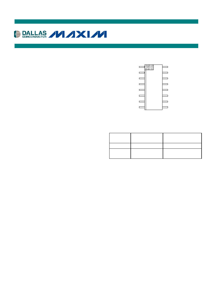
PIN CONFIGURATION
16
15
14
13
12
11
10
9
N.C.
N.C.
P1
P2
P3
P4
RSTZ
P5
N.C.
P0
V
CC
I/O
GND
N.C.
P7
P6
1
2
3
4
5
6
7
8
150-mil SO
ORDERING INFORMATION
PART
TEMP
RANGE
PACKAGE
DS2408S -40∞C to +85∞C 16-Pin SO, 150 mil
DS2408S
/T&R
-40
∞C to +85∞C
Tape-and-Reel of
DS2408S
DESCRIPTION
The DS2408 is an 8-channel, programmable I/O 1-Wire chip. PIO outputs are configured as open-drain
and provide an on resistance of 100
W max. A robust PIO channel-access communication protocol ensures
that PIO output-setting changes occur error-free. A data-valid strobe output can be used to latch PIO logic
states into external circuitry such as a D/A converter (DAC) or microcontroller data bus.
DS2408 operation is controlled over the single-conductor 1-Wire bus. Device communication follows the
standard Dallas Semiconductor 1-Wire protocol. Each DS2408 has its own unalterable and unique 64-bit
ROM registration number that is factory lasered into the chip. The registration number guarantees unique
identification and is used to address the device in a multidrop 1-Wire net environment. Multiple DS2408
devices can reside on a common 1-Wire bus and can operate independently of each other. The DS2408
also supports 1-Wire conditional search capability based on PIO conditions or power-on-reset activity;
the conditions to cause participation in the conditional search are programmable. The DS2408 has an
optional V
CC
supply connection. When an external supply is absent, device power is supplied parasitically
from the 1-Wire bus. When an external supply is present, PIO states are maintained in the absence of the
1-Wire bus power source. The RSTZ signal is configurable to serve as either a hard-wired reset for the
PIO output or as a strobe for external circuitry to indicate that a PIO write or PIO read has completed.
1 of 36
061604
1-Wire is a registered trademark of Dallas Semiconductor.

DS2408
ABSOLUTE MAXIMUM RATINGS*
P0 to P7, RSTZ, I/O Voltage to GND
-0.5V, +6V
P0 to P7, RSTZ, I/O combined sink current
20mA
Operating Temperature Range
-40∞C to +85∞C
Junction Temperature
+150∞C
Storage Temperature Range
-55∞C to +125∞C
Lead Temperature (10s)
See J-STD-020A specification
* This is a stress rating only and functional operation of the device at these or any other conditions
above those indicated in the operation sections of this specification is not implied. Exposure to
absolute maximum rating conditions for extended periods of time may affect reliability.
ELECTRICAL CHARACTERISTICS
(V
CC
= 0V or
≥ V
PUP
, T
A
= -40∞C or +85∞C.)
PARAMETER SYMBOL CONDITIONS
MIN TYP MAX UNITS
Standard speed
2.8
5.25
1-Wire Pullup
Voltage
V
PUP
Overdrive speed
3.3
5.25
V
Standby Supply
Current
I
CCS
V
CC
at V
PUP,
I/O pin at 0.3V
1 µA
I/O Pin General Data
1-Wire Pullup
Resistance
R
PUP
(Notes 1, 2)
2.2
k
W
Input Capacitance
C
IO
(Notes 3, 4)
1200
pF
Input Load Current
I
L
I/O pin at V
PUP,
V
CC
at 0V
1 µA
High-to-Low
Switching Threshold
V
TL
(Notes 4, 5, 6)
0.5
3.2 V
Input-Low Voltage
V
IL
(Notes 1, 7)
0.30
V
Low-to-High
Switching Threshold
V
TH
(Notes 4, 5, 8)
0.8
3.4 V
Switching Hysteresis
V
HY
(Notes 9, 4)
0.16
0.73
V
Output-Low Voltage
at 4mA
V
OL
(Note 10)
0.4 V
Standard speed, R
PUP
=
2.2k
W
5
Overdrive speed, R
PUP
=
2.2k
W
2
Recovery Time
(Note 1)
t
REC
Overdrive speed, Directly
prior to reset pulse; R
PUP
= 2.2k
W
5
µs
Standard speed
0.5
5
Rising-Edge Hold-off
Time (Notes 11, 4)
t
REH
Overdrive speed
0.5
2
µs
Standard speed
65
Timeslot Duration
(Notes 1, 12)
t
SLOT
Overdrive speed
10
µs
2 of 36

DS2408
PARAMETER SYMBOL CONDITIONS
MIN TYP MAX UNITS
I/O Pin, 1-Wire Reset, Presence-Detect Cycle
Standard speed, V
PUP
>
4.5V
480
720
Standard speed
660
720
Reset-Low Time
(Notes 1, 12)
t
RSTL
Overdrive speed
53
80
µs
Standard speed
15
60
Presence-Detect High
Time (Note 12)
t
PDH
Overdrive speed
2
7
µs
Standard speed, V
PUP
>
4.5V
1
5
Standard speed
1
8
Presence-Detect Fall
Time (Note 13)
t
FPD
Overdrive speed
1
µs
Standard speed, V
PUP
>
4.5V
60
240
Standard speed
60
280
Presence-Detect Low
Time (Note 12)
t
PDL
Overdrive speed
7
27
µs
Standard speed, V
PUP
>
4.5V
65
75
Standard speed
68
75
Presence-Detect
Sample Time (Note 1)
t
MSP
Overdrive speed
8
9
µs
I/O Pin, 1-Wire Write
Standard speed
60
120
Write-0 Low Time
(Notes 1, 12)
t
W0L
Overdrive speed
8
13
µs
Standard speed
5
15 -
e
Write-1 Low Time
(Notes 1, 12, 14)
t
W1L
Overdrive speed
1
1.8 -
e
µs
Standard speed
15
60
Write Sample Time
(Slave Sampling)
(Note 12)
t
SLS
Overdrive speed
1.8
8
µs
I/O Pin, 1-Wire Read
Standard speed
5
15 -
d
Read-Low Time
(Notes 1, 15)
t
RL
Overdrive speed
1
1.8 -
d
µs
Standard speed
15
60
Read-0 Low Time
(Data From Slave)
(Note 12)
t
SPD
Overdrive speed
1.8
8
µs
Standard speed
t
RL
+
d
15
Read-Sample Time
(Notes 1, 12, 15)
t
MSR
Overdrive speed
t
RL
+
d
1.8
µs
P0 to P7, RSTZ Pin
Input-Low Voltage
V
IL
(Notes 1, 7)
0.30
V
Input-High Voltage
V
IH
V
X
= max (V
PUP
,V
CC
)
(Note 1)
V
X
- 0.8
5.25 V
Output-Low Voltage
at 4mA
V
OL
(Note 10)
0.4 V
Leakage Current
I
LP
5.25V at the pin
1
µA
Output Fall Time
t
FPIO
(Notes 4, 16)
100
ns
Minimum-Sensed
PIO Pulse
t
PWMIN
(Notes 4, 17)
1
5 µs
3 of 36

DS2408
Note 1:
System Requirement
Note 2:
Maximum allowable pullup resistance is a function of the number of 1-Wire devices in the
system and 1-Wire recovery times. The specified value here applies to systems with only one
device and with the minimum 1-Wire recovery times. For more heavily loaded systems, an
active pullup such as that found in the DS2480B may be required.
Note 3:
If a 2.2k
W resistor is used to pull up the data line to V
PUP
, 5µs after power has been applied,
the parasite capacitance does not affect normal communications.
Note 4:
Guaranteed by design--not production tested.
Note 5:
V
TL
, V
TH
are a function of the internal supply voltage.
Note 6:
Voltage below which, during a falling edge on I/O, a logic '0' is detected.
Note 7:
The voltage on I/O needs to be less or equal to V
ILMAX
whenever the master drives the line
low.
Note 8:
Voltage above which, during a rising edge on I/O, a logic '1' is detected.
Note 9:
After V
TH
is crossed during a rising edge on I/O, the voltage on I/O has to drop by V
HY
to be
detected as logic '0'.
Note 10: The I-V characteristic is linear for voltages less than 1V.
Note 11: The earliest recognition of a negative edge is possible at t
REH
after V
TH
has been reached
before.
Note 12: Highlighted numbers are NOT in compliance with the published 1-Wire standards. See
comparison table below.
Note 13: Interval during the negative edge on I/O at the beginning of a presence detect pulse between
the time at which the voltage is 90% of V
PUP
and the time at which the voltage is 10% of
V
PUP
.
Note 14: e represents the time required for the pullup circuitry to pull the voltage on I/O up from V
IL
to V
TH
.
Note 15: d represents the time required for the pullup circuitry to pull the voltage on I/O up from V
IL
to the input high threshold of the bus master.
Note 16: Interval during the device-generated negative edge on any PIO pin or the RSTZ pin between
the time at which the voltage is 90% of V
PUP
and the time at which the voltage is 10% of
V
PUP
. PIO pullup resistor = 2.2k
W.
Note 17: Width of the narrowest pulse which trips the activity latch (for any PIO pin) or causes a reset
(for the RSTZ pin). For a pulse duration t
PW
: If t
PW
< t
PWMIN(min)
, the pulse will be rejected. If
t
PWMIN(min)
< t
PW
< t
PWMIN(max)
, the pulse may or may not be rejected. If t
PW
> t
PWMIN(max)
the
pulse will be recognized and latched.
Note 18: Maximum instantaneous pulldown current through all port pins and the RSTZ pin combined.
No requirement for current balance among different pins.
STANDARD VALUES
DS2408 VALUES
STANDARD
SPEED
OVERDRIVE
SPEED
STANDARD
SPEED
OVERDRIVE
SPEED
PARAMETER
NAME
MIN MAX MIN MAX MIN MAX MIN MAX
t
SLOT
(incl. t
REC
)
61µs (undef.) 7µs (undef.)
65µs
1)
(undef.) 10µs
(undef.)
t
RSTL
480µs (undef.) 48µs 80µs 660µs
720µs
53µs
80µs
t
PDH
15µs 60µs 2µs 6µs 15µs 60µs 2µs 7µs
t
PDL
60µs 240µs 8µs 24µs 60µs 280µs
7µs
27µs
t
W0L
60µs 120µs 6µs 16µs 60µs 120µs 8µs
13µs
t
SLS
, t
SPD
15µs 60µs 2µs 6µs 15µs 60µs 1.8µs
8µs
1)
Intentional change, longer recovery-time requirement due to modified 1-Wire front end.
4 of 36

DS2408
PIN DESCRIPTION
PIN
NAME
DESCRIPTION
1 N.C.
Not
Connected
2 P0
I/O Pin of Channel 0. Logic input/open-drain output with 100
W maximum
on-resistance; 0V to 5.25V operating range. Power-on default is
indeterminate. If it is application-critical for the outputs to power up in the
"off" state, the user should attach an appropriate power-on-reset circuit or
supervisor IC to the RSTZ pin.
3 V
CC
Optional Power Supply Input. Range 2.8V to 5.25V; must be tied to GND
if not used.
4
I/O
1-Wire Interface. Open-drain, requires external pullup resistor.
5 GND
Ground
6 N.C.
Not
Connected
7
P7
I/O Pin of Channel 7. Same characteristics as P0.
8
P6
I/O Pin of Channel 6. Same characteristics as P0.
9
P5
I/O Pin of Channel 5. Same characteristics as P0.
10 RSTZ
SW configurable PIO reset input (
RST
) or open-drain strobe output
(
STRB
). When configured as
RST
, a LOW input sets all PIO outputs to
the "off" state by setting all bits in the PIO Output Latch State Register.
When configured as
STRB
, an output strobe will occur after a PIO write
(see Channel-Access Write command) or after a PIO Read (see Channel-
Access Read command). The power-on default function of this pin is
RST
.
11
P4
I/O pin of channel 4; same characteristics as P0
12
P3
I/O pin of channel 3; same characteristics as P0
13
P2
I/O pin of channel 2; same characteristics as P0
14
P1
I/O pin of channel 1; same characteristics as P0
15 N.C.
Not
connected
16 N.C.
Not
connected
APPLICATION
The DS2408 is a multipurpose device. Typical applications include port expander for microcontrollers,
remote multichannel sensor/actuator, communication and control unit of a microterminal, or as network
interface of a microcontroller. Typical application circuits and communication examples are found later
in this data sheet (Figures 17 to 22).
OVERVIEW
5 of 36
Figure 1 shows the relationships between the major function blocks of the DS2408. The device has two
main data components: 1) 64-bit lasered ROM, and 2) 64-bit register page of control and status registers.
Figure 2 shows the hierarchical structure of the 1-Wire protocol. The bus master must first provide one of
the eight ROM function commands: 1) Read ROM, 2) Match ROM, 3) Search ROM, 4) Conditional
Search ROM, 5) Skip ROM, 6) Overdrive-Skip ROM, 7) Overdrive-Match ROM, or 8) Resume. Upon
completion of an Overdrive ROM command byte executed at standard speed, the device will enter
overdrive mode, where all subsequent communication occurs at a higher speed. The protocol required for
these ROM function commands is described in Figure 12. After a ROM function command is success-
fully executed, the control functions become accessible and the master may provide any one of the five
available commands. The protocol for these control commands is described in Figure 8. All data is read
and written least significant bit first.

DS2408
Figure 1. DS2408 BLOCK DIAGRAM
V
CC
64-BIT
LASERED ROM
CRC16
GENERATOR
REGISTER
PAGE
REGISTER
FUNCTION
CONTROL
1-WIRE
FUNCTION
CONTROL
PORT
FUNCTION
CONTROL
I/O
GND
PARASITE POWER
INTERNAL V
CC
PORT
INTER-
FACE
RSTZ
P0
P1
P2
P3
P4
P5
P6
P7
Figure 2. HIERARCHICAL STRUCTURE FOR 1-Wire PROTOCOL
1-Wire Net
Other
Devices
Bus
Master
Command
Level:
1-Wire ROM Function
Commands
DS2408-Specific
Control Function
Commands
DS2408
Available
Commands:
Read ROM
Match ROM
Search ROM
Skip ROM
Conditional Search
ROM
Overdrive Match
Overdrive Skip
Resume
Read PIO Registers
Channel Access Read
Channel Access Write
Write Conditional
Search Register
Reset Activity Latches
Data Field
Affected:
64-BIT ROM, RC-FLAG
64-BIT ROM, RC-FLAG
64-BIT ROM, RC-FLAG
RC-FLAG
64-BIT ROM, RC-FLAG, Port Status,
Cond. Search Settings,
64-BIT ROM, RC-FLAG, OD-Flag
RC-FLAG, OD-Flag
RC-FLAG
PIO Registers
Port Input Latches
Port Output Latches
Conditional Search Register
Activity Latches
Cmd.
Codes:
33h
55h
F0h
CCh
ECh
69h
3Ch
A5h
F0h
F5h
5Ah
CCh
C3h
6 of 36

DS2408
PARASITE POWER
The DS2408 can derive its power entirely from the 1-Wire bus by storing energy on an internal capacitor
during periods of time when the signal line is high. During low times the device continues to operate from
this "parasite" power source until the 1-Wire bus returns high to replenish the parasite (capacitor) supply.
If power is available, the V
CC
pin should be connected to the external voltage supply.
Figure 3. 64-BIT LASERED ROM
MSB
LSB
8-BIT
CRC CODE
48-BIT SERIAL NUMBER
8-BIT FAMILY
CODE (29h)
MSB
LSB
MSB
LSB
MSB
LSB
64-BIT LASERED ROM
Each DS2408 contains a unique ROM code that is 64 bits long. The first 8 bits are a 1-Wire family code.
The next 48 bits are a unique serial number. The last eight bits are a CRC of the first 56 bits. See Figure 3
for details. The 1-Wire CRC is generated using a polynomial generator consisting of a shift register and
XOR gates as shown in Figure 4. The polynomial is X
8
+ X
5
+ X
4
+ 1. Additional information about the
Dallas 1-Wire Cyclic Redundancy Check is available in Application Note 27.
The shift register bits are initialized to 0. Then, starting with the least significant bit of the family code,
one bit at a time is shifted in. After the eighth
bit of the family code has been entered, the serial number is
entered. After the serial number has been entered, the shift register contains the CRC value. Shifting in
the eight bits of CRC returns the shift register to all 0s.
Figure 4. 1-Wire CRC GENERATOR
X
0
X
1
X
2
X
3
X
4
X
5
X
6
X
7
X
8
POLYNOMIAL = X
8
+ X
5
+ X
4
+ 1
1
st
STAGE
2
nd
STAGE
3
rd
STAGE
4
th
STAGE
6
th
STAGE
5
th
STAGE
7
th
STAGE
8
th
STAGE
INPUT DATA
REGISTER ACCESS
The registers needed to operate the DS2408 are organized as a Register Page, as shown in Figure 5. All
registers are volatile, i. e., they lose their state when the device is powered down. PIO, Conditional
Search, and Control/Status registers are read/written using the device level Read PIO Registers and Write
Conditional Search Register commands described in subsequent sections and Figure 8 of this document.
7 of 36

DS2408
Figure 5. DS2408 REGISTER ADDRESS MAP
ADDRESS RANGE
ACCESS TYPE
DESCRIPTION
0000h to 0087h
R
Undefined Data
0088h R
PIO
Logic
State
0089h
R
PIO Output Latch State Register
008Ah
R
PIO Activity Latch State Register
008Bh
R/W
Conditional Search Channel Selection Mask
008Ch
R/W
Conditional Search Channel Polarity Selection
008Dh R/W
Control/Status
Register
008Eh to 008Fh
R
These Bytes Always Read FFh
PIO Logic-State Register
The logic state of the PIO pins can be obtained by reading this register using the Read PIO Registers
command. Reading this register does not generate a signal at the RSTZ pin, even if it is configured as
STRB
. See the Channel-Access commands description for details on
STRB
.
PIO Logic State Register Bitmap
ADDR
b7 b6 b5 b4 b3 b2 b1 b0
0088h
P7 P6 P5 P4 P3 P2 P1 P0
This register is read-only. Each bit is associated with the pin of the respective PIO channel as shown in
Figure 6. The data in this register is sampled at the last (most significant) bit of the byte that proceeds
reading the first (least significant) bit of this register. See the Read PIO Registers command description
for details.
PIO Output Latch State Register
The data in this register represents the latest data written to the PIO through the Channel-access Write
command. This register is read using the Read PIO Registers command. Reading this register does not
generate a signal at the RSTZ pin, even if it is configured as
STRB
. See the Channel-access commands
description for details on
STRB
. This register is not affected if the device reinitializes itself after an ESD
hit.
PIO Output Latch State Register Bitmap
ADDR
b7 b6 b5 b4 b3 b2 b1 b0
0089h PL7 PL6 PL5 PL4 PL3 PL2 PL1 PL0
This register is read-only. Each bit is associated with the output latch of the respective PIO channel as
shown in Figure 6.
The flip-flops of this register will power up in a random state. If the chip has to power up with all PIO
channels off, a LOW pulse must be generated on the RSTZ pin, e.g., by means of an open-drain CPU
supervisor chip (see Figure 20). When using an RC circuit to generate the power-on reset, make sure that
RSTZ is NOT configured as strobe output (ROS bit in control/status register 008Dh needs to be 0).
8 of 36

DS2408
PIO Activity Latch State Register
The data in this register represents the current state of the PIO activity latches. This register is read using
the Read PIO Registers command. Reading this register does not generate a signal at the RSTZ pin, even
if it is configured as
STRB
. See the Channel-access commands description for details on
STRB
.
PIO Activity Latch State Register Bitmap
ADDR
b7 b6 b5 b4 b3 b2 b1 b0
008Ah AL7 AL6 AL5 AL4 AL3 AL2 AL1 AL0
This register is read-only. Each bit is associated with the activity latch of the respective PIO channel as
shown in Figure 6. This register is cleared to 00h by a power-on reset, by a low pulse on the RSTZ pin
(only if RSTZ is configured as
RST
input), or by successful execution of the Reset Activity Latches
command.
Figure 6. CHANNEL I/O AND RSTZ SIMPLIFIED LOGIC DIAGRAM
PIO
OUTPUT
LATCH
PIO ACTIVITY
LATCH
EDGE
DETECTOR
PORT
FUNCTION
CONTROL
TO ACTIVITY LATCH
STATE REGISTER
TO PIO LOGIC
STATE REGISTER
TO PIO
OUTPUT LATCH
STATE REG.
R
Q
D
D
Q
S
Q
Q
"1"
CLR ACT LATCH
ROS
STRB
CHANNEL
I/O PIN
RSTZ
PIN
DATA
CLOCK
POWER ON
RESET
9 of 36

DS2408
Conditional Search Channel Selection Mask Register
The data in this register controls whether a PIO channel qualifies for participation in the conditional
search command. To include one or more of the PIO channels, the bits in this register that correspond to
those channels need to be set to 1. This register can only be written through the Write Conditional Search
Registers command.
Conditional Search Channel Selection Mask Register Bitmap
ADDR
b7 b6 b5 b4 b3 b2 b1 b0
008Bh SM7 SM6 SM5 SM4 SM3 SM2 SM1 SM0
This register is read/write. Each bit is associated with the respective PIO channel as shown in Figure 7.
This register is cleared to 00h by a power-on reset
Conditional Search Channel Polarity Selection Register
The data in this register specifies the polarity of each selected PIO channel for the device to respond to
the conditional search command. Within a PIO channel, the data source may be either the channel's input
signal (pin) or the channel's activity latch, as specified by the PLS bit in the Control/Status register at ad-
dress 008Dh. This register can only be written through the Write Conditional Search Registers command.
Conditional Search Channel Polarity Selection Register Bitmap
ADDR
b7 b6 b5 b4 b3 b2 b1 b0
008Ch SP7 SP6 SP5 SP4 SP3 SP2 SP1 SP0
This register is read/write. Each bit is associated with the respective PIO channel as shown in Figure 7.
This register is cleared to 00h by a power-on reset.
Figure 7. Conditional Search Logic
AL7
P7
PLS
SP0
SM0
CT
SM7
SP7
AL0
P0
CSR
INPUT FROM
CHANNELS 1 TO 6
(NOT SHOWN)
CHANNEL 0
CHANNEL 7
10 of 36

DS2408
Control/Status Register
The data in this register reports status information, determines the function of the RSTZ pin and further
configures the device for conditional search. This register can only be written through the Write Condi-
tional Search Registers command.
Control/Status Register Bitmap
ADDR
b7 b6 b5 b4 b3 b2 b1 b0
008Dh VCCP
0
0
0
PORL ROS CT
PLS
This register is read/write. Without V
CC
supply, this register reads 08h after a power-on reset. The func-
tional assignments of the individual bits are explained in the table below. Bits 4 to 6 have no function;
they will always read 0 and cannot be set to 1.
Control/Status Register Details
BIT DESCRIPTION
BIT(S)
DEFINITION
PLS: Pin or Activity
Latch Select
b0
Selects either the PIO pins or the PIO activity latches as input for the
conditional search.
0: pin selected (default)
1: activity latch selected
CT: Conditional Search
Logical Term
b1
Specifies whether the data of two or more channels needs to be OR'ed
or AND'ed to meet the qualifying condition for the device to respond to a
conditional search. If only a single channel is selected in the channel
selection mask (008Bh) this bit is a don't care.
0: bitwise OR (default)
1: bitwise AND
ROS: RSTZ Pin Mode
Control
b2
Configures RSTZ as either RST input or STRB output
0: configured as RST input (default)
1: configured as STRB output
PORL: Power-On Reset
Latch
b3
Specifies whether the device has performed a power-on reset. This bit
can only be cleared to 0 under software control. As long as this bit is 1
the device will always respond to a conditional search.
VCCP: V
CC
Power
Status (Read-Only)
b7 For
V
CC
powered operation the V
CC
pin needs to be tied to a voltage
source
≥ V
PUP
.
0:
V
CC
pin is grounded
1:
V
CC
-powered operation
The interaction of the various signals that determine whether the device responds to a conditional search
is illustrated in Figure 7. The selection mask SM selects the participating channels. The polarity selection
SP determines for each channel whether the channel signal needs to be 1 or 0 to qualify. The PLS bit
determines whether all channel signals are taken from the activity latches or I/O pins. The signals of all
channels are fed into an AND gate as well as an OR gate. The CT bit finally selects the AND'ed or
OR'ed result as the conditional search response signal CSR.
Note on CT bit:
OR
The qualifying condition is met if the input (pin state or activity latch) for one or more selected
channels matches the corresponding polarity.
AND For the qualifying condition to be met, the input (pin state or activity latch) for every selected
channel must match the corresponding polarity.
11 of 36

DS2408
Figure 8-1. CONTROL FUNCTIONS FLOW CHART
Bus Master TX
TA1 (T7:T0), TA2 (T15:T8)
Y
N
F0h
Read PIO Reg.?
Y
N
Address
< 90h?
To Figure 8
2
nd
Part
From Figure 8
2
nd
Part
Bus Master TX Control
Function Command
To ROM Functions
Flow Chart (Figure 12)
From ROM Functions
Flow Chart (Figure 12)
DS2408 sets Register
Address = (T15:T0)
Bus Master RX Data Byte
from Register Address
Bus Master RX CRC16
of Command, Address,
Data Bytes
Bus Master
RX "1"s
Y
N
DS2408 Incre-
ments Address
Counter
Y
Y
N
N
Master
TX Reset?
Address
< 90h?
Master
TX Reset?
Master
TX Reset?
Y
N
Note:
To read the three PIO state and latch
register bytes, the target address should
be 0088h. Returned data for a target
address <0088h is undefined.
Address
= 88h?
Y
N
DS2408 Samples
PIO Pin Status
1)
Note 1)
See the command
description for the
exact timing of the
PIO pin sampling.
12 of 36

DS2408
Figure 8-2. CONTROL FUNCTIONS FLOW CHART
From Figure 8
1
st
Part
To Figure 8
1
st
Part
To Figure 8
3
rd
Part
From Figure 8
3
rd
Part
F5h
Channel Access
Read?
DS2408 Samples
PIO Pin Status
PIO Sample
Counter = 0
Y
N
Sample Count
= 31?
Y
N
Master
TX Reset?
Bus Master RX
PIO Pin Status
DS2408 Increments
PIO Sample Counter
DS2408 Samples
PIO Pin Status
Bus Master RX
PIO Pin Status
PIO Sample
Counter = 0
DS2408 Samples
PIO Pin Status
Bus Master RX
CRC16 of Command
and 32 Bytes of PIO
Pin Status (1
st
Pass)
CRC16 of 32 Bytes
of PIO Pin Status
(Subsequent Passes)
Y
N
5Ah
Channel Access
Write?
Bus Master TX new
PIO Output Data Byte
Bus Master TX
inverted new PIO
Output Data Byte
Transmission
OK?
DS2408 Updates
PIO Pin Status
Bus Master RX
Confirmation AAh
DS2408 Samples
PIO Pin Status
Bus Master RX
PIO Pin Status
Y
N
Master
TX Reset?
N
Y
Bus Master
RX "1"s
Y
N
Master
TX Reset?
Note 1)
See the command
description for the
exact timing of the
PIO pin sampling
and updating.
Note 2)
If the RSTZ pin is con-
figured as output, a
STRB\ is generated
during the first two bits
of this byte.
N
Y
2)
2)
1)
1)
1)
1)
2)
1)
13 of 36

DS2408
Figure 8-3. CONTROL FUNCTIONS FLOW CHART
From Figure 8
2
nd
Part
To Figure 8
2
nd
Part
CCh
Write C. Search
Reg.?
Bus Master TX
TA1 (T7:T0), TA2 (T15:T8)
N
Y
8Bh
£ Address £
8Dh?
Y
N
Master
TX Reset?
Bus Master TX
Data Byte
DS2408 Incre-
ments Address
Counter
DS2408 Copies
Data to Register
Y
N
C3h
Reset Activity
Latches?
DS2408 Clears all
PIO Activity Latches
Bus Master RX
Confirmation AAh
Y
N
Master
TX Reset?
Y
N
Master
TX Reset?
Bus Master
RX "1"s
Y
N
Master
TX Reset?
Note:
To read 8Bh to 8Dh
use the Read PIO
Registers command.
Y
N
14 of 36

DS2408
CONTROL FUNCTION COMMANDS
Once a ROM function command is completed, the Control Function Commands can be issued. The
Control Functions Flow Chart (Figure 8) describes the protocols necessary for accessing the PIO
channels and the special function registers of the DS2408. The communication between the master and
the DS2408 takes place either at standard speed (default, OD = 0) or at overdrive speed (OD = 1). If not
explicitly set into the overdrive mode, the device operates at standard speed.
Read PIO Registers [F0h]
The Read PIO Registers command is used to read any of the device's registers. After issuing the
command, the master must provide the 2-byte target address. After these two bytes, the master reads data
beginning from the target address and may continue until address 008Fh. If the master continues reading,
it will receive an inverted 16-bit CRC of the command, address bytes, and all data bytes read from the
initial starting byte through the end of the register page. This CRC16 is the result of clearing the CRC
generator and then shifting in the command byte followed by the two address bytes and the data bytes
beginning at the first addressed location and continuing through to the last byte of the register page. After
the bus master has received the CRC16, the DS2408 responds to any subsequent read-time slots with
logical 1's until a 1-Wire Reset command is issued. If this command is issued with target address 0088h
(PIO Logic State Register), the PIO sampling takes place during the transmission of the MS bit of TA2. If
the target address is lower than 0088h, the sampling takes place while the master reads the MS bit from
address 0087h.
Channel-Access Read [F5h]
In contrast to reading the PIO logical state from address 88h, this command reads the status in an endless
loop. After 32 bytes of PIO pin status the DS2408 inserts an inverted CRC16 into the data stream, which
allows the master to verify whether the data was received error-free. A Channel-Access Read can be
terminated at any time with a 1-Wire Reset.
Figure 9. CHANNEL-ACCESS READ TIMING
IO (1-Wire)
STRB\
Example - Sampled State = 72h
MS 2 bits of pre-
vious byte (8Dh)
LS 2 bits of data
byte (72h)
t
SPD
t
SPD
t
SPD
Sampling Point
Notes:
1) The "previous byte" could be the command code, the data byte resulting from the previous PIO
sample, or the MS byte of a CRC16. The example shows a read-1 time slot.
2) The sample point timing also applies to the Channel-access Write command, with the "previous byte"
being the write confirmation byte (AAh). No
STRB
pulse results when sampling occurs during a
Channel-Access Write command.
15 of 36

DS2408
The status of all eight PIO channels is sampled at the same time. The first sampling occurs during the last
(most significant) bit of the command code F5h. While the master receives the MSB of the PIO status
(i.e., the status of pin P7) the next sampling occurs and so on until the master has received 31 PIO
samples. Next, the master receives the inverted CRC16 of the command byte and 32 PIO samples (first
pass) or the CRC of 32 PIO samples (subsequent passes). While the last (most significant) bit of the CRC
is transmitted the next PIO sampling takes place. The delay between the beginning of the time slot and
the sampling point is independent of the bit value being transmitted and the data direction (see Figure 9).
If the RSTZ pin is configured as
STRB
, a strobe signal will be generated during the transmission of the
first two (least significant) bits of PIO data. The strobe can signal a FIFO or a microcontroller to apply
the next data byte at the PIO for the master to read through the 1-Wire line.
Case #1 - MS Bit of new PIO state is 0
Example - Old State = 39h, New state = 72h
Case #2 - MS Bit of new PIO state is 1
Example - Old State = 72h, New state = 93h
Channel-Access Write [5Ah]
The Channel-Access Write command is the only way to write to the PIO output-latch state register
(address 0089h), which controls the open-drain output transistors of the PIO channels. In an endless loop
this command first writes new data to the PIO and then reads back the PIO status. The implicit read-after-
write can be used by the master for status verification or for a fast communication with a microcontroller
that is connected to the port pins and RSTZ for synchronization. A Channel-Access Write can be termi-
nated at any time with a 1-Wire Reset.
Figure 10. CHANNEL-ACCESS WRITE TIMING
IO (1-Wire)
PIO
STRB\
39h
72h
t
SLS
t
SPD
t
SPD
MS 2 bits of inverted
new-state byte (8Dh)
LS 2 bits of confir-
mation byte (AAh)
MS 2 bits of inverted
new-state byte (6Ch)
LS 2 bits of confir-
mation byte (AAh)
72h
93h
t
SPD
t
SPD
V
TH
Note:
Both examples assume that the RSTZ pin is configured as
STRB
output. If RSTZ is configured as
RST
input (default), the RSTZ pin needs to be tied high (to V
CC
or V
PUP
) for the Channel-Access Write to
function properly. Leaving the pin floating will force the output transistors of the PIO channels to the
"off" state and the PIO output latches will all read "1". See Figure 6 for a schematic of the logic.
After the command code the master transmits a byte that determines the new state of the PIO output
transistors. The first (least significant) bit is associated to P0. To switch the output transistor off (non-
conducting) the corresponding bit value is 1. To switch the transistor on that bit needs to be 0. This way
the data byte transmitted as the new PIO output state arrives in its true form at the PIO pins. To protect
the transmission against data errors, the master has to repeat the new PIO byte in its inverted form. Only
if the transmission was successful will the PIO status change. The actual transition at the PIO to the new
state occurs during the last (most significant) bit of the inverted new PIO data byte and depends on the
polarity of that bit, as shown in Figure 10. If this bit is a 1, the transition begins after t
SLS
is expired; in
case of a 0, the transition begins at the end of the time slot, when the V
TH
threshold is crossed. To inform
the master about the successful change of the PIO status, the DS2408 transmits a confirmation byte with
16 of 36

DS2408
the data pattern AAh. If the RSTZ pin is configured as
STRB
, a strobe signal will be generated during the
transmission of the first two (least significant) bits of the confirmation byte. The strobe can signal a FIFO
or a microcontroller to read the new data byte from the PIO. While the last bit of the confirmation byte is
transmitted, the DS2408 samples the status of the PIO pins, as shown in Figure 9, and sends it to the
master. Depending on the data, the master can either continue writing more data to the PIO or issue a 1-
Wire reset to end the command.
Write Conditional Search Register [CCh]
This command is used to tell the DS2408 the conditions that need to be met for the device to respond to a
Conditional Search command, to define the function of the RSTZ pin and to clear the power-on reset flag.
After issuing the command the master sends the 2-byte target address, which must be a value between
008Bh and 008Dh. Next the master sends the byte to be written to the addressed cell. If the address was
valid, the byte is immediately written to its location in the register page. The master now can either end
the command by issuing a 1-Wire reset or send another byte for the next higher address. Once register
address 008Dh has been written, any subsequent data bytes will be ignored. The master has to send a 1-
Wire reset to end the command. Since the Write Conditional Search Register flow does not include any
error-checking for the new register data, it is important to verify correct writing by reading the registers
using the Read PIO Registers command.
Reset Activity Latches [C3h]
Each PIO channel includes an activity latch that is set whenever there is a state transition at a PIO pin.
This change may be caused by an external event/signal or by writing to the PIO. Depending on the
application there may be a need to reset the activity latch after having captured and serviced an external
event. Since there is only read access to the PIO Activity Latch State Register, the DS2408 supports a
special command to reset the latches. After having received the command code, the device resets all
activity latches simultaneously. There are two ways for the master to verify the execution of the Reset
Activity Latches command. The easiest way is to start reading from the 1-Wire line right after the
command code is transmitted. In this case the master will read AAh bytes until it sends a 1-Wire reset.
The other way to verify execution is to read register address 008Ah.
1-WIRE BUS SYSTEM
The 1-Wire bus is a system that has a single bus master and one or more slaves. In all instances the
DS2408 is a slave device. The bus master is typically a microcontroller or PC. For small configurations
the 1-Wire communication signals can be generated under software control using a single port pin. For
multisensor networks, the DS2480B 1-Wire line driver chip or serial port adapters based on this chip
(DS9097U series) are recommended. This simplifies the hardware design and frees the microprocessor
from responding in real time.
The discussion of this bus system is broken down into three topics: hardware configuration, transaction
sequence, and 1-Wire signaling (signal types and timing). The 1-Wire protocol defines bus transactions in
terms of the bus state during specific time slots that are initiated on the falling edge of sync pulses from
the bus master.
HARDWARE CONFIGURATION
The 1-Wire bus has only a single line by definition; it is important that each device on the bus be able to
drive it at the appropriate time. To facilitate this, each device attached to the 1-Wire bus must have open
drain or tri-state outputs. The 1-Wire port of the DS2408 is open-drain with an internal circuit equivalent
to that shown in Figure 11.
17 of 36

DS2408
Figure 11. HARDWARE CONFIGURATION
OPEN-DRAIN
PORT PIN
RX = RECEIVE
TX = TRANSMIT
100
W
MOSFET
V
PUP
RX
TX
TX
RX
DATA
SEE
TEXT
SIMPLE BUS MASTER
DS2408 1-Wire PORT
R
PUP
DS2480B
+5V
HOST CPU
VDD
POL
RXD
TXD
VPP
1-W
NC
GND
SERIAL IN
SERIAL OUT
SERIAL
PORT
TO 1-Wire DATA
DS2480B BUS MASTER
A multidrop bus consists of a 1-Wire bus with multiple slaves attached. At standard speed the 1-Wire bus
has a maximum data rate of 15.3kbps. Communication speed for 1-Wire devices can be typically boosted
to 142kbps by activating the overdrive mode; however, the maximum overdrive data rate for the DS2408
is 100kbps. The value of the pullup resistor primarily depends on the network size and load conditions.
For most applications the optimal value of the pullup resistor will be approximately 2.2k
W for standard
speed and 1.5k
W for overdrive speed.
The idle state for the 1-Wire bus is high. If for any reason a transaction needs to be suspended, the bus
MUST be left in the idle state if the transaction is to resume. If this does not occur and the bus is left low
for more than 16µs (overdrive speed) or more than 120µs (standard speed), one or more devices on the
bus may be reset. With the DS2408 the bus must be left low for no longer than 13µs at overdrive speed to
ensure that none of the slave devices on the 1-Wire bus performs a reset. The DS2408 communicates
properly when used in conjunction with a DS2480B 1-Wire driver and serial port adapters that are based
on this driver chip. When operating the device in overdrive or below 4.5V, some 1-Wire I/O timing
values must be modified (see EC table).
18 of 36

DS2408
TRANSACTION SEQUENCE
The protocol for accessing the DS2408 through the 1-Wire port is as follows:
ß Initialization
ß ROM Function Command
ß Control Function Command
ß Transaction/Data
Illustrations of the transaction sequence for the various control function commands are found later in this
document.
INITIALIZATION
All transactions on the 1-Wire bus begin with an initialization sequence. The initialization sequence
consists of a reset pulse transmitted by the bus master followed by presence pulse(s) transmitted by the
slave(s). The presence pulse lets the bus master know that the DS2408 is on the bus and is ready to
operate. For more details, see the 1-Wire Signaling section.
ROM FUNCTION COMMANDS
Once the bus master has detected a presence, it can issue one of the seven ROM function commands. All
ROM function commands are eight bits long. A list of these commands follows (see the flowchart in
Figure 12).
Read ROM [33h]
This command allows the bus master to read the DS2408's 8-bit family code, unique 48-bit serial number,
and 8-bit CRC. This command can only be used if there is a single device on the bus. If more than one
slave is present on the bus, a data collision will occur when all slaves try to transmit at the same time
(open drain will produce a wired-AND result). The resultant family code and 48-bit serial number will
result in a mismatch of the CRC.
Match ROM [55h]
The Match ROM command, followed by a 64-bit ROM sequence, allows the bus master to address a spe-
cific DS2408 on a multidrop bus. Only the DS2408 that exactly matches the 64-bit ROM sequence will
respond to the following control function command. All slaves that do not match the 64-bit ROM se-
quence will wait for a reset pulse. This command can be used with either single or multiple devices on the
bus.
Search ROM [F0h]
When a system is initially brought up, the bus master might not know the number of devices on the
1-Wire bus or their 64-bit ROM codes. The Search ROM command allows the bus master to use a
process of elimination to identify the 64-bit ROM codes of all slave devices on the bus. The search ROM
process is the repetition of a simple three-step routine: read a bit, read the complement of the bit, then
write the desired value of that bit. The bus master performs this simple, three-step routine on each bit of
the ROM. After one complete pass, the bus master knows the contents of the ROM in one device. The
remaining number of devices and their ROM codes may be identified by additional passes. See
Application Note 187 for a detailed discussion on the Search ROM command process including a
software example.
Conditional Search [ECh]
19 of 36
The Conditional Search ROM command operates similarly to the Search ROM command except that only
devices fulfilling the specified condition will participate in the search. The condition is specified by the
Conditional Search channel and polarity selection (addresses 008Bh, 008Ch), the bit functions CT and

DS2408
PLS of the Control/Status Register (address 008Dh), and the state of the PIO channels. See Figure 7 for a
description of the Conditional Search logic. The device also responds to the Conditional Search if the
PORL bit is set. The Conditional Search ROM provides an efficient means for the bus master to deter-
mine devices on a multidrop system that have to signal an important event, such as a state change at a
PIO pin caused by an external signal. After each pass of the conditional search that successfully deter-
mined the 64-bit ROM for a specific device on the multidrop bus, that particular device can be individu-
ally accessed as if a Match ROM had been issued, since all other devices will have dropped out of the
search process and will be waiting for a reset pulse.
Skip ROM [CCh]
This command can save time in a single-drop bus system by allowing the bus master to access the control
functions without providing the 64-bit ROM code. If more than one slave is present on the bus and a
Read command is issued following the Skip ROM command, data collision will occur on the bus as
multiple slaves transmit simultaneously (open-drain pulldowns will produce a wired-AND result).
Resume Command [A5h]
In a typical application the DS2408 can be accessed several times to complete a control or adjustment
function. In a multidrop environment this means that the 64-bit ROM sequence of a Match ROM com-
mand has to be repeated for every access. To maximize the data throughput in a multidrop environment,
the Resume Command function is implemented. This function checks the status of the RC flag and, if it is
set, directly transfers control to the control functions, similar to a Skip ROM command. The only way to
set the RC flag is through successfully executing the Match ROM, Search ROM, Conditional Search
ROM, or Overdrive-Match ROM command. Once the RC flag is set, the device can be repeatedly
accessed through the Resume Command function. Accessing another device on the bus will clear the RC
flag, preventing two or more devices from simultaneously responding to the Resume Command function.
Skip ROM [3Ch]
On a single-drop bus this command can save time by allowing the bus master to access the control
functions without providing the 64-bit ROM code. Unlike the normal Skip ROM command, the
Overdrive Skip ROM sets the DS2408 in the overdrive mode (OD = 1). All communication following
this command has to occur at overdrive speed until a reset pulse of minimum 480µs duration resets all
devices on the bus to standard speed (OD = 0). When issued on a multidrop bus this command will set all
overdrive-supporting devices into overdrive mode. To subsequently address a specific overdrive-
supporting device, a reset pulse at overdrive speed has to be issued followed by a Match ROM or Search
ROM command sequence. This will speed up the time for the search process. If more than one slave
supporting overdrive is present on the bus and the Overdrive Skip ROM command is followed by a Read
command, data collision will occur on the bus as multiple slaves transmit simultaneously (open-drain
pulldowns will produce a wired-AND result).
Overdrive Match ROM [69h]
The Overdrive Match ROM command followed by a 64-bit ROM sequence transmitted at overdrive
speed allows the bus master to address a specific DS2408 on a multidrop bus and to simultaneously set it
in overdrive mode. Only the DS2408 that exactly matches the 64-bit ROM sequence will respond to the
subsequent control function command. Slaves already in overdrive mode from a previous Overdrive Skip
or Match command will remain in overdrive mode. All overdrive-capable slaves will return to standard
speed at the next Reset Pulse of minimum 480µs duration. The Overdrive Match ROM command can be
used with either single or multiple devices on the bus.
20 of 36

DS2408
Figure 12-1. ROM FUNCTIONS FLOW CHART
From Figure 12
2
nd
Part
To Control Functions
Flow Chart (Figure 8)
Master TX Bit 0
Master TX Bit 63
Master TX Bit 1
RC = 1
DS2408 TX
CRC Byte
DS2408 TX
Serial Number
(6 Bytes)
DS2408 TX
Family Code
(1 Byte)
Bit 0
Match?
Y
N
Bit 1
Match?
Y
N
Bit 63
Match?
Y
N
DS2408 TX Bit 0
DS2408 TX Bit 0
Master TX Bit 0
DS2408 TX Bit 1
DS2408 TX Bit 1
Master TX Bit 1
DS2408 TX Bit 63
DS2408 TX Bit 63
Master TX Bit 63
RC = 1
Bit 0
Match?
Y
N
Bit 1
Match?
Y
N
Bit 63
Match?
Y
N
To Figure 12
2
nd
Part
RC = 0
RC = 0
RC = 0
RC = 0
Y
Y
Y
Y
N
F0h
Search ROM
Command?
N
55h
Match ROM
Command?
N
ECh
Cond. Search
Command?
N
33h
Read ROM
Command?
To Figure 12
2
nd
Part
From Control Functions
Flow Chart (Figure 8)
Bus Master TX ROM
Function Command
DS2408 TX
Presence Pulse
OD
Reset Pulse?
N
Y
OD = 0
Bus Master TX
Reset Pulse
From Figure 12, 2
nd
Part
Condition Met?
Y
N
DS2408 TX Bit 0
DS2408 TX Bit 0
Master TX Bit 0
DS2408 TX Bit 1
DS2408 TX Bit 1
Master TX Bit 1
DS2408 TX Bit 63
DS2408 TX Bit 63
Master TX Bit 63
RC = 1
Bit 0
Match?
Y
N
Bit 1
Match?
Y
N
Bit 63
Match?
Y
N
21 of 36

DS2408
Figure 12-2. ROM FUNCTIONS FLOW CHART
From Figure 12
1
st
Part
From Figure 12
1
st
Part
To Figure 12, 1
st
Part
RC = 1 ?
N
Y
RC = 0 ; OD = 1
Master TX Bit 0
Master TX Bit 63
Master TX Bit 1
RC = 1
Bit 0
Match?
Y
N
Bit 1
Match?
Y
N
Bit 63
Match?
Y
N
Y
N
69h
Overdrive Match
ROM?
RC = 0 ; OD = 1
Master
TX Reset ?
Y
N
Master
TX Reset ?
N
Y
Y
N
3Ch
Overdrive
Skip ROM?
Y
N
A5h
Resume
Command?
RC = 0
Y
N
CCh
Skip ROM
Command?
To Figure 12
1
st
Part
22 of 36

DS2408
1-WIRE SIGNALING
The DS2408 requires strict protocols to ensure data integrity. The protocol consists of four types of
signaling on one line: Reset Sequence with Reset Pulse and Presence Pulse, Write-Zero, Write-One, and
Read-Data. Except for the presence pulse, the bus master initiates all these signals. The DS2408 can
communicate at two different speeds, standard speed, and overdrive speed. If not explicitly set into the
overdrive mode, the DS2408 will communicate at standard speed. While in overdrive mode, the fast
timing applies to all waveforms.
To get from idle to active, the voltage on the 1-Wire line needs to fall from V
PUP
below the V
TL
threshold.
To get from active to idle, the voltage needs to rise from V
ILMAX
past the V
TH
threshold. The V
ILMAX
voltage is relevant for the DS2408 when determining a logical level, not triggering any events.
Figure 13 shows the initialization sequence required to begin any communication with the DS2408. A
Reset Pulse followed by a Presence Pulse indicates the DS2408 is ready to receive data, given the correct
ROM and control function command. If the bus master uses slew-rate control on the falling edge, it must
pull down the line for t
RSTL
+ t
F
to compensate for the edge. A t
RSTL
duration of 480µs or longer will exit
the overdrive mode returning the device to standard speed. If the DS2408 is in overdrive mode and t
RSTL
is no longer than 80µs the device will remain in overdrive mode.
Figure 13. INITIALIZATION PROCEDURE "RESET AND PRESENCE PULSES"
RESISTOR
MASTER
DS2408
t
RSTL
t
PDL
t
RSTH
t
PDH
MASTER TX "RESET PULSE" MASTER RX "PRESENCE PULSE"
V
PUP
V
IHMASTER
V
TH
V
TL
V
ILMAX
0V
e
t
F
t
REC
t
MSP
After the bus master has released the line it goes into receive mode (RX). The 1-Wire bus is then pulled
to V
PUP
via the pullup resistor or, in case of a DS2480B driver, by active circuitry. When the V
TH
threshold is crossed, the DS2408 waits for t
PDH
and then transmits a Presence Pulse by pulling the line
low for t
PDL
. To detect a presence pulse, the master must test the logical state of the 1-Wire line at t
MSP
.
The t
RSTH
window must be at least the sum of t
PDHMAX
, t
PDLMAX
, and t
RECMIN
. Immediately after t
RSTH
is
expired, the DS2408 is ready for data communication. In a mixed population network, t
RSTH
should be
extended to a minimum of 480µs at standard speed and 48µs at overdrive speed to accommodate other 1-
Wire devices.
23 of 36

DS2408
Read/Write Time Slots
Data communication with the DS2408 takes place in time slots, which carry a single bit each. Write time
slots transport data from bus master to slave. Read time slots transfer data from slave to master. The
definitions of the write and read time slots are illustrated in Figure 14.
All communication begins with the master pulling the data line low. As the voltage on the 1-Wire line
falls below the threshold V
TL
, the DS2408 starts its internal time base. The tolerance of the slave time
base creates a slave-sampling window, which stretches from t
SLSMIN
to t
SLSMAX
. The voltage on the data
line at the sampling point determines whether the DS2408 decodes the time slot as 1 or 0.
Master-to-Slave
For a write-one time slot, the voltage on the data line must have crossed the V
THMAX
threshold after the
write-one low time t
W1LMAX
has expired. For a write-zero time slot, the voltage on the data line must stay
below the V
THMIN
threshold until the write-zero low time t
W0LMIN
has expired. For most reliable
communication, the voltage on the data line should not exceed V
ILMAX
during the entire t
W0L
window.
After the V
THMAX
threshold has been crossed, the DS2408 needs a recovery time t
REC
before it is ready for
the next time slot.
Figure 14. READ/WRITE TIMING DIAGRAM
Write-One Time Slot
V
PUP
V
IHMASTER
V
TH
V
TL
V
ILMAX
0V
DS2408
Sampling
Window
t
SLSMIN
t
F
t
SLOT
t
W1L
t
SLSMAX
e
Write-Zero Time Slot
t
REC
V
PUP
V
IHMASTER
V
TH
V
TL
V
ILMAX
0V
DS2408
Sampling
Window
t
SLSMIN
t
F
t
SLOT
t
SLSMAX
t
W0L
24 of 36

DS2408
Read-Data Time Slot
RESISTOR
MASTER
DS2408
t
REC
V
PUP
V
IHMASTER
V
TH
V
TL
V
ILMAX
0V
Master
Sampling
Window
t
SPDMIN
d
t
F
t
SLOT
t
RL
t
MSR
t
SPDMAX
Slave-to-Master
A read-data time slot begins like a write-one time slot. The voltage on the data line must remain below
V
TLMIN
until the read low time t
RL
has expired. During the t
RL
window, when responding with a 0, the
DS2408 starts pulling the data line low; its internal timing generator determines when this pulldown ends
and the voltage starts rising again. When responding with a 1, the DS2408 does not hold the data line low
at all, and the voltage starts rising as soon as t
RL
is over.
The sum of t
RL
+
d (rise time) on one side and the internal timing generator of the DS2408 on the other
side define the master sampling window (t
MSRMIN
to t
MSRMAX
) in which the master must perform a read
from the data line. For most reliable communication, t
RL
should be as short as permissible and the master
should read close to but no later than t
MSRMAX
. After reading from the data line, the master must wait until
t
SLOT
is expired. This guarantees sufficient recovery time t
REC
for the DS2408 to get ready for the next
time slot.
Improved Network Behavior
In a 1-Wire environment, line termination is possible only during transients controlled by the bus master
(1-Wire driver). 1-Wire networks therefore are susceptible to noise of various origins. Depending on the
physical size and topology of the network, reflections from end points and branch points can add up or
cancel each other to some extent. Such reflections are visible as glitches or ringing on the 1-Wire
communication line. Noise coupled onto the 1-Wire line from external sources can also result in signal
glitching. A glitch during the rising edge of a time slot can cause a slave device to lose synchronization
with the master and, as a consequence, result in a Search ROM command coming to a dead end or cause a
device level command to abort. For better performance in network applications, the DS2408 uses a new
1-Wire front end, which makes it less sensitive to noise and also reduces the magnitude of noise injected
by the slave device itself.
The 1-Wire front end of the DS2408 differs from traditional slave devices in four characteristics.
1) The falling edge of the presence pulse has a controlled slew rate. This provides a better match to the
line impedance than a digitally switched transistor, converting the high-frequency ringing known
from traditional devices into a smoother low-bandwidth transition. The slew rate control is specified
by the parameter t
FPD
, which has different values for standard and overdrive speed.
2) There is additional lowpass filtering in the circuit that detects the falling edge at the beginning of a
time slot. This reduces the sensitivity to high-frequency noise. This additional filtering does not apply
at overdrive speed.
25 of 36

DS2408
3) The input buffer was designed with hysteresis. If a negative glitch crosses V
TH
but doesn't go below
V
TH
- V
HY
, it will not be recognized (Figure 15, Case A). The hysteresis is effective at any 1-Wire
speed.
4) There is a time window specified by the rising edge hold-off time t
REH
during which glitches will be
ignored, even if they extend below the V
TH
- V
HY
threshold (Figure 15, Case B, t
GL
< t
REH
). Deep
voltage droops or glitches that appear late after crossing the V
TH
threshold and extend beyond the t
REH
window cannot be filtered out and will be taken as the beginning of a new time slot (Figure 15, Case
C, t
GL
≥ t
REH
).
Figure 15. NOISE SUPPRESSION SCHEME
V
PUP
V
TH
V
HY
0V
t
REH
t
GL
t
REH
t
GL
Case A
Case C
Case B
CRC GENERATION
The DS2408 has two different types of cyclic redundancy checks (CRCs). One CRC is an 8-bit type and
is stored in the most significant byte of the 64-bit ROM. The bus master can compute a CRC value from
the first 56 bits of the 64-bit ROM and compare it to the value stored within the DS2408 to determine if
the ROM data has been received error free. The equivalent polynomial function of this CRC is X
8
+ X
5
+
X
4
+ 1. This 8-bit CRC is received in the true (noninverted) form. It is computed at the factory and lasered
into the ROM.
The other CRC is a 16-bit type, generated according to the standardized CRC16-polynomial function X
16
+ X
15
+ X
2
+ 1. This CRC is used for error detection when reading data through the end of the register
page using the Read PIO Registers command, for fast verification of the data transfer when writing to or
reading from the scratchpad, and when reading from the PIO using the Channel-access Read command.
In contrast to the 8-bit CRC, the 16-bit CRC is always communicated in the inverted form. A CRC-
generator inside the DS2408 chip (Figure 16) calculates a new 16-bit CRC as shown in the command
flow chart of Figure 8. The bus master compares the CRC value read from the device to the one it
calculates from the data and decides whether to continue with an operation or to reread the portion of the
data with the CRC error.
With the Read PIO Registers flow chart, the 16-bit CRC value is the result of shifting the command byte
into the cleared CRC generator, followed by the 2 address bytes and the data bytes beginning at the target
address and ending with the last byte of the register page, address 008Fh.
With the initial pass through the Channel-access Read command flow, the CRC is generated by first
clearing the CRC generator and then shifting in the command code followed by 32 bytes of PIO pin data.
Subsequent passes through the command flow will generate a 16-bit CRC that is the result of clearing the
CRC generator and then shifting in 32 bytes read from the PIO pins. For more information on generating
CRC values see Application Note 27.
26 of 36

DS2408
Figure 16. CRC-16 HARDWARE DESCRIPTION AND POLYNOMIAL
POLYNOMIAL = X
16
+ X
15
+ X
2
+ 1
X
0
X
1
X
2
X
3
X
4
X
5
X
6
X
7
X
8
X
9
X
10
X
11
X
12
X
13
X
14
X
15
X
16
1
st
STAGE
2
nd
STAGE
3
rd
STAGE
4
th
STAGE
6
th
STAGE
5
th
STAGE
7
th
STAGE
8
th
STAGE
9
th
STAGE
10
th
STAGE
11
th
STAGE
12
th
STAGE
13
th
STAGE
14
th
STAGE
15
th
STAGE
16
th
STAGE
INPUT DATA
CRC
OUTPUT
Figure 17. DS2408 AS SLAVE INTERFACE FOR MICROCONTROLLER
VCC
DS80C520
P1.0
3
P1.1
4
P1.2
5
P1.3
6
P1.4
7
P1.5
8
P1.6
9
P1.7
10
RST
12
P3 .7 / RD
22
P3 .6 / WR
21
P3.5/T1
20
P3.4/T0
19
P3 .3 / INT1
18
P3 .2 / INT0
17
P3.1/TXD0
16
P3.0/RXD0
15
EA
42
XTAL2
23
XTAL1
24
RTCX2
27
RTCX1
28
P2.6/AD14
36
P2.5/AD13
35
P2.4/AD12
34
P2.3/AD11
33
P2.2/AD10
32
P2.7/AD15
37
P2.1/AD9
31
P2.0/AD8
30
PSEN
38
ALE
39
P0.7/AD7
43
P0.6/AD6
44
P0.5/AD5
45
P0.4/AD4
46
P0.3/AD3
47
P0.2/AD2
48
P0.1/AD1
49
P0.0/AD0
50
47U
DS2408
P0
2
P1
14
P2
13
P3
12
P4
11
P5
9
P6
8
P7
7
10
GND
5
VCC
3
IO
4
PULLUP PROVIDED BY CPU
8051 Equiv CPU
GND
VCC
1W
RSTZ
The data direction (upload/download) is determined by application-specific data protocol.
27 of 36
DS2408
Figure 18. DS2408 AS SLAVE INTERFACE FOR INTELLIGENT DISPLAY
47
DS9503
1
2
5
6
3
4
47U
VCC
LEDK
16
LEDA
15
D7
14
D6
13
D5
12
D4
11
D3
10
D2
9
D1
8
D0
7
STB
6
R/ W
5
D/ C
4
CONTRAST
3
VCC
2
GND
1
VCC
10K
10
9
8
7
6
5
4
3
2
1
VCC
DS2408
P0
2
P1
14
P2
13
P3
12
P4
11
P5
9
P6
8
P7
7
10
GND
5
VCC
3
IO
4
Local iButton Probe
LCD Display
Up
Down
Select
5VDC
GND
1W
RSTZ
A
C
M160
1B
1
6
X
1
D
i
s
p
l
a
y
w
i
t
h
B
a
ck
L
i
g
h
t
VCC
Figure 19. DS2408 AS MICROCONTROLLER PORT EXPANDER
DS2408
IO
4
VCC
3
GND
5
10
P7
7
P6
8
P5
9
P4
11
P3
12
P2
13
P1
14
P0
2
VC
C
2.
2
K
VCC
PIC12C508
OSC2/P4
3
OSC1/P5
2
P0
7
P1
6
P2/CK
5
CLR/P3
4
GND
8
VCC
1
VCC
MICROCONTROLLER
WITH FEW I/O PINS
RSTZ
24 I/O LINES OR
3 BYTE-WIDE
BUSES FROM A
SINGLE PIN
IO
4
VCC
3
GND
5
10
P7
7
P6
8
P5
9
P4
11
P3
12
P2
13
P1
14
P0
2
VCC
RSTZ
DS2408
IO
4
VCC
3
GND
5
10
P7
7
P6
8
P5
9
P4
11
P3
12
P2
13
P1
14
P0
2
VCC
RSTZ
DS2408
28 of 36

DS2408
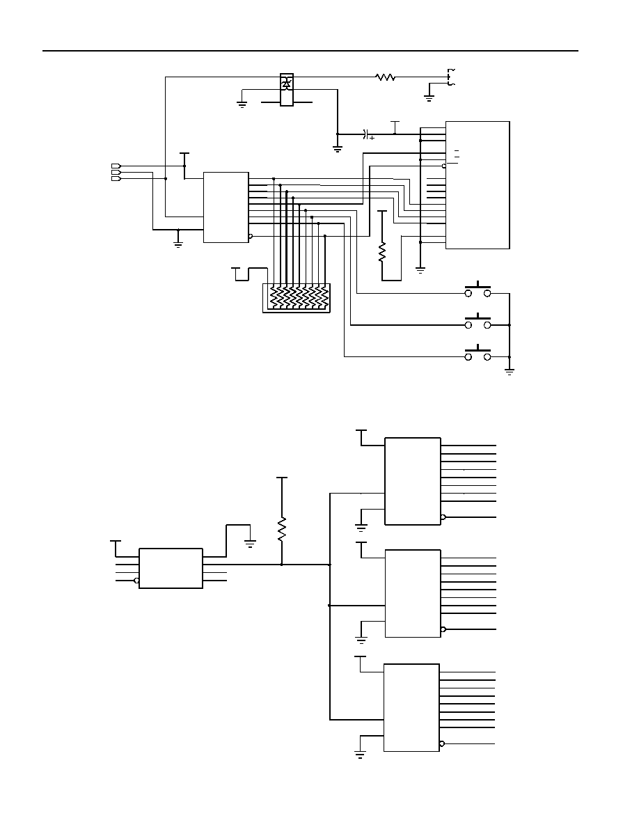
Figure 20. DS2408 AS µC-OPERATED KEYBOARD SCANNER
VCC
10k
W
10
9
8
7
6
5
4
3
2
1
10U
DS2408
P0
2
P1
14
P2
13
P3
12
P4
11
P5
9
P6
8
P7
7
10
GND
5
VCC
3
IO
4
POR Circuit
To More Switch Rows
(Up to 4 x 4, 3 x 5 or 2 x 6)
GND
VCC
RST
GND
DS1811
VCC
VCC
1W
RSTZ
The DS1811 has
an internal pull-up
resistor of 5.5 k
W
Figure 21. DS2408 AS PARASITE-POWERED PUSH-BUTTON SENSOR
BAT54
0.1U
100k
1 2 3 4 5 6 7 8 9 10
DS2408
P0
2
P1
14
P2
13
P3
12
P4
11
P5
9
P6
8
P7
7
10
GND
5
VCC
3
IO
4
SWITCHES OR PUSH-BUTTONS
Parasite
Power
VCC
1W
GND
RSTZ
29 of 36

DS2408
Figure 22. DS2408 AS MULTIPURPOSE SENSOR/ACTUATOR
10k
W
10
9
8
7
6
5
4
3
2
1
VCC
BSS-84
5V
1N4004
47U
VCC
OPTOISO
1
2
4
5
6
1k
W
470
W
VCC
LED
DS2408
P0
2
P1
14
P2
13
P3
12
P4
11
P5
9
P6
8
P7
7
10
GND
5
VCC
3
IO
4
4mA
8mA
1W
VCC
GND
RSTZ
SWITCHES
OR PUSH-
BUTTONS
ISOLATED
OUTPUT
DRY
CONTACT
LED INDI-
CATOR
VCC
30 of 36

DS2408
Command-Specific 1-Wire Communication Protocol--Legend
SYMBOL DESCRIPTION
RST
1-Wire Reset Pulse generated by master.
PD
1-Wire Presence Pulse generated by slave.
Select
Command and data to satisfy the ROM function protocol.
RPR
Command "Read PIO Registers".
CAR Command
"Channel-Access
Read".
CAW Command
"Channel-Access
Write".
WCS
Command "Write Conditional Search Register".
RAL
Command "Reset Activity Latches".
TA
Target Address TA1, TA2.
<data>
Transfer of an undetermined amount of data.
CRC16\
Transfer of an inverted CRC16.
FF loop
Indefinite loop where the master reads FF bytes.
AA loop
Indefinite loop where the master reads AA bytes.
<32 samples>,
CRC16\ loop
Indefinite loop where the master reads 32 PIO samples followed by an inverted CRC16.
<new state>, <new
state\>
Transfer of 2 bytes, where the second byte is the bit-inverse of the first byte. The first
byte will be taken as the new PIO state.
AAh, <read back>
Transfer of 2 bytes, where the first byte is a constant (AAh) and the second byte is the
current PIO state.
<new state>,
<invalid>
Transfer of 2 bytes, where the second byte is NOT the bit-inverse of the first byte.
Command-Specific 1-Wire Communication Protocol--Color Codes
Master to slave
Slave to master
Read PIO Registers (Success)
RST
PD
Select
RPR TA
<data>
CRC16\ FF loop
Read PIO Registers (Fail Address)
RST
PD
Select
RPR TA
FF loop
Channel-Access Read (Cannot Fail)
RST
PD
Select
CAR <32 samples>, CRC16\ loop
31 of 36

DS2408
Channel-Access Write (Success)
RST
PD
Select
CAW <new state>, <new state\>
AAh, <read back>
Channel-Access Write (Fail New State)
Loop
RST
PD
Select
CAW <new state>, <invalid>
FF loop
Write Conditional Search Register (Success)
RST
PD
Select
WCS TA
<data>
FF loop
Write Conditional Search Register (Fail Address)
RST
PD
Select
WCS TA
FF loop
Reset Activity Latches (Cannot Fail)
RST
PD
Select
RAL
AA loop
COMMUNICATION EXAMPLES
The examples in this section demonstrate the use of ROM and control functions in typical situations. The
first two examples are related to Figure 17. They show how to write to the PIO with readback for
verification or for receiving an immediate response (example 1) and how to read from the PIO in an
endless loop (example 2). The third example assumes a network of multiple DS2408s where each of the
devices is connected to 8 pushbuttons, as in Figure 21.
Example 1
Task: Write to the PIO with readback for verification or for receiving an immediate response.
This task is broken into the following steps:
1) Configure RSTZ as
STRB
output.
2) Verify configuration setting.
3) Write to the PIO and read back the response.
With only a single DS2408 connected to the bus master, the communication is as follows:
32 of 36
MASTER MODE
DATA (LSB FIRST)
COMMENTS
Step 1
TX
(Reset)
Reset pulse
RX (Presence)
Presence
pulse
TX
CCh
Issue Skip ROM command
TX
CCh
Issue Write Conditional Search Register
command
TX
8Dh
TA1, target address = 8Dh
TX
00h
TA2, target address = 008Dh
TX
04h
Write byte to Control/Status Register

DS2408
MASTER MODE
DATA (LSB FIRST)
COMMENTS
TX (Reset)
Reset
pulse
RX (Presence)
Presence
pulse
Step 2
TX
CCh
Issue Skip ROM command
TX
F0h
Issue Read PIO Registers command
TX
8Dh
TA1, target address = 8Dh
TX
00h
TA2, target address = 008Dh
RX
84h
Read Control/Status Register and verify
TX (Reset)
Reset
pulse
RX (Presence)
Presence
pulse
Step 3
TX
CCh
Issue Skip ROM command
TX 5Ah
Issue
Channel-access
Write
command
TX
<PIO output byte>
Write byte to PIO
TX
<inverted PIO output byte>
Write inverted byte to PIO
(--)
(--)
DS2408 updates PIO status if transmission
was OK
RX
AAh
Read for verification (AAh = success)
(--)
(--)
DS2408 samples PIO pin status
RX
<PIO pin status byte>
Read PIO pin status
TX
<PIO output byte>
Write byte to PIO (next byte)
TX
<inverted PIO output byte>
Write inverted byte to PIO (next byte)
RX
AAh
Read for verification (AAh = success)
RX
<PIO pin status byte>
Read PIO pin status
(--) (--)
Repeat the previous 4 steps with more PIO
output data as needed in the application.
TX (Reset)
Reset
pulse
RX (Presence)
Presence
pulse
When using this communication example to send data to a remote microcontroller, as in Figure 17,
synchronization between the master and the remote microcontroller can be maintained by transmitting
data packets that begin with a length byte and end with a CRC16. See Application Note 114, section
"UNIVERSAL DATA PACKET" for details.
Example 2
Task: Read from the PIO in an endless loop.
This task is broken into the following steps:
1) Configure RSTZ as
STRB
output.
2) Verify configuration setting.
3) Read from the PIO.
With only a single DS2408 connected to the bus master, the communication is as follows:
MASTER MODE
DATA (LSB FIRST)
COMMENTS
Step 1
TX
(Reset)
Reset pulse
RX (Presence)
Presence
pulse
TX
CCh
Issue Skip ROM command
TX CCh
Issue Write Conditional Search Register
command
TX
8Dh
TA1, target address = 8Dh
TX
00h
TA2, target address = 008Dh
33 of 36

DS2408
MASTER MODE
DATA (LSB FIRST)
COMMENTS
TX
04h
Write byte to Control/Status Register
TX (Reset)
Reset
pulse
RX (Presence)
Presence
pulse
Step 2
TX
CCh
Issue Skip ROM command
TX
F0h
Issue Read PIO Registers command
TX
8Dh
TA1, target address = 8Dh
TX
00h
TA2, target address = 008Dh
RX
84h
Read Control/Status Register and verify
TX (Reset)
Reset
pulse
RX (Presence)
Presence
pulse
Step 3
TX
CCh
Issue Skip ROM command
TX
F5h
Issue Channel-access Read command
(--)
(--)
DS2408 samples PIO pin status
RX
<PIO pin status byte>
Read PIO pin status
(--) (--)
Repeat the previous 2 steps until the master
has received a total of 32 bytes of PIO pin
status
RX
<2 bytes CRC16>
Read CRC16
(--) (--)
PIO pin status and CRC loop can be
continued as long as the application requires.
TX (Reset)
Reset
pulse
RX (Presence)
Presence
pulse
When using this communication example to read data from a remote microcontroller, as in Figure 17,
synchronization between the remote microcontroller and the master can be maintained by transmitting
data packets that begin with a length byte and end with a CRC16. See Application Note 114, section
"UNIVERSAL DATA PACKET" for details.
Example 3
Task: Detect the specific DS2408 where the button was pressed and identify the pin to which the
pushbutton is connected. This task is broken into the following steps:
1) Configure the conditional search and verify configuration setting.
2) Switch off all channel output transistors.
3) Clear the activity latches.
4) Search until a pushbutton is pressed.
5) Identify device and pushbutton; reset activity latches.
The device has to respond to the conditional search if the activity latch of at least one of the 8 channels is
set. This requires the following setup data for the conditional search registers:
Channel Selection Mask, select all channels
Þ FFh
Channel Polarity Selection, select logic 1 for all channels
Þ FFh
34 of 36

DS2408
Control/Status register,
Source is Activity Latch
Þ PLS = 1
Term is OR
Þ CT = 0
RSTZ = inactive (input)
Þ ROS = 0
Clear Power-On Reset Latch
Þ PORL = 0
The resulting setup data for the Control/Status Register is 01h.
For each DS2408 in the application, perform the following initialization:
MASTER MODE
DATA (LSB FIRST)
COMMENTS
Step 1
TX
(Reset)
Reset pulse
RX (Presence)
Presence
pulse
TX
55h
Issue Match ROM command
TX
<8 byte ROM ID>
Send ROM ID of the device to be accessed
TX CCh
Issue Write Conditional Search Register
command
TX
8Bh
TA1, target address = 8Bh
TX
00h
TA2, target address = 008Bh
TX
FFh
Write Channel Selection Mask
TX
FFh
Write Channel Polarity Selection
TX
01h
Write Control/Status Register
TX (Reset)
Reset
pulse
RX (Presence)
Presence
pulse
TX
A5h
Issue Resume command
TX
F0h
Issue Read PIO Registers command
TX
8Bh
TA1, target address = 8Bh
TX
00h
TA2, target address = 008Bh
RX
<FFh, FFh, 81h>
Read Registers and verify
TX (Reset)
Reset
pulse
RX (Presence)
Presence
pulse
Step 2
TX
A5h
Issue Resume command
TX 5Ah
Issue
Channel-access
Write
command
TX
FFh
Write byte to PIO
TX
00h
Write inverted byte to PIO
(--) (--)
DS2408 switches off all channel output
transistors if transmission was OK
RX
AAh
Read for verification (AAh = success)
RX
FFh
Read PIO pin status and verify; FFh = OK
TX (Reset)
Reset
pulse
RX (Presence)
Presence
pulse
Step 3
TX
A5h
Issue Resume command
TX
C3
Issue Reset Activity Latch command
RX
AAh
Read for verification (AAh = success)
TX (Reset)
Reset
pulse
RX (Presence)
Presence
pulse
35 of 36

DS2408
36 of 36
After all DS2408s are initialized, perform the search process below as an endless loop:
MASTER MODE
DATA (LSB FIRST)
COMMENTS
Step 4
TX
(Reset)
Reset pulse
RX (Presence)
Presence
pulse
TX
ECh
Issue Conditional Search ROM command
RX <2
bits>
Read 2 bits; if both bits are 1, no push button
has been pressed; in this case return to Step
4. If the bit pattern is 01 or 10 or 00, a push
button has been pressed; in this case
continue with Step 5.
Step 5
TX
<1 bits>
Identify and select the LS bit of the ROM ID
of the DS2408 that has responded to the
Conditional Search.
RX <2
bits>
Read 2 bits; this relates to the next bit of the
ROM ID of the participating device(s).
TX <1
bits>
Identify and select the next bit of the ROM ID
of the DS2408 that has responded to the
Conditional Search.
(--) (--)
Repeat the previous 2 steps until one device
has been identified and accessed. (see Note
1)
TX
F0h
Issue Read PIO Registers command
TX
88h
TA1, target address = 88h
TX
00h
TA2, target address = 0000h
RX <8
data
bytes>
Read register page; the data in the Activity
Latch State Register tells which button has
been pressed.
RX <2
bytes
CRC16>
Read CRC16 and verify correct data
transmission.
TX (Reset)
Reset
pulse
RX (Presence)
Presence
pulse
TX
A5h
Issue Resume command
TX
C3
Issue Reset Activity Latch command
RX
AAh
Read for verification (AAh = success)
(--) (--)
Now, as the device and push button are
identified and the Activity Latch is cleared,
continue at Step 4.
Note 1: For a full description of the Search Algorithm see Application Note 187.