Äîêóìåíòàöèÿ è îïèñàíèÿ www.docs.chipfind.ru
1 of 17
051106
GENERAL DESCRIPTION
The DS25LV02 provides data storage and serial
number identification for battery packs. The low-
voltage Dallas 1-Wire
Ò interface enables serial
communication on a single battery contact and the
64-bit unique serial number allows multidrop
networking and identification of individual devices.
The 1024-bit EPROM memory is organized as 4
pages of 32 bytes each and supports storage of
battery cell characteristics, charging voltage, current
and temperature parameters, as well as battery pack
manufacturing data. CRC verification provides data
integrity during communication. The EPROM pages
are in-circuit writable and can be individually locked
to protect data. The DS25LV02 is designed to be
completely backward-compatible with the DS2502 for
existing designs.
APPLICATIONS
Cell Phones/Smartphones
Digital Cameras
MP3 Players
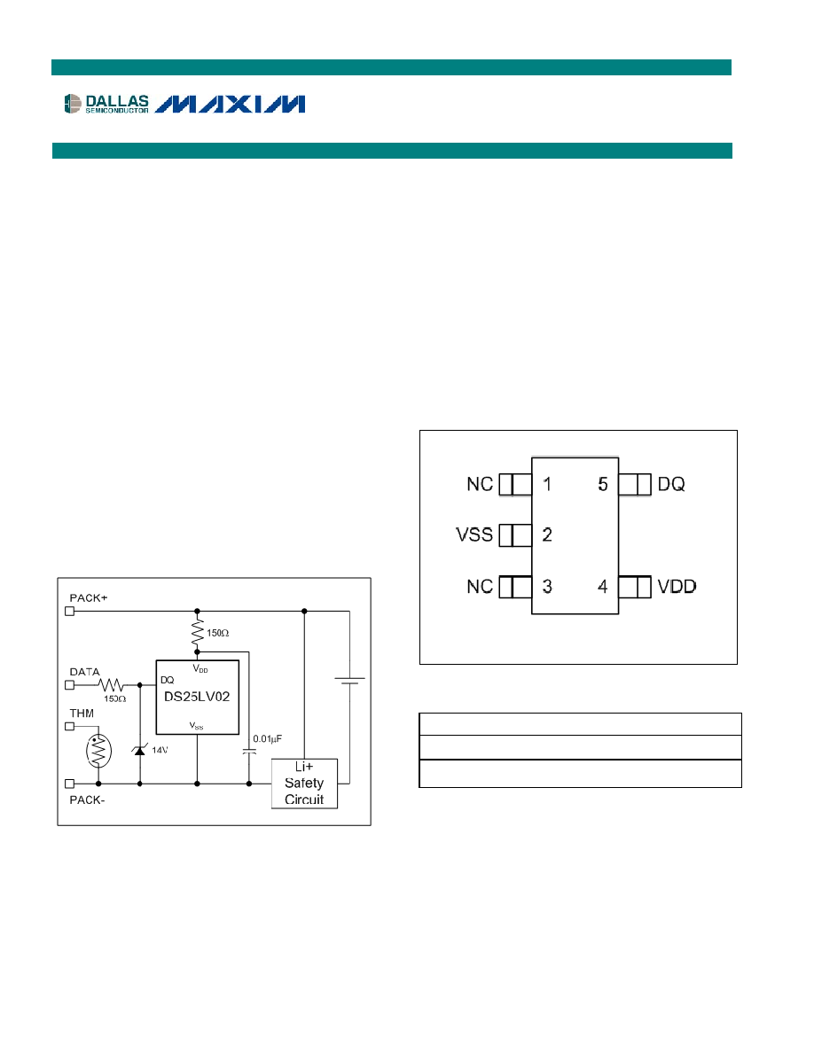
TYPICAL APPLICATION CIRCUIT
FEATURES
§ 128 Bytes of EPROM Storage Organized into
Four Separately Lockable Pages
§ Backward-Compatible with DS2502
§ Dallas 1-Wire Interface
§ Input Logic Thresholds Compatible with 1.8V
I/O Supply Rail
§ Unique 64-Bit Serial Number
§ Operates with V
DD
as Low as 2.2V
§ Tiny, Thin SOT-23 Package
PIN CONFIGURATION
TOP VIEW
5-Pin Thin-SOT (TSOT)
ORDERING INFORMATION
PART TEMP
RANGE
PIN-PACKAGE
DS25LV02R+U
-30°C to +85°C
5 Thin SOT
DS25LV02R+T&
R
-30°C to +85°C
5 Thin SOT in
Tape-and-Reel
+Denotes lead-free package.
1-Wire is a registered trademark of Dallas Semiconductor.
Certain commands, modes, and registers are capitalized for
clarity.
DS25LV02
Low-Voltage 1024-Bit EPROM
www.maxim-ic.com

DS25LV02: Low-Voltage 1024-Bit EPROM
2 of 17
ABSOLUTE MAXIMUM RATINGS
Voltage Range on DQ, Relative to V
SS
-0.3V to +12V
Voltage Range on V
DD
, Relative to V
SS
-0.3V to +6V
Operating Temperature Range
-30°C to +85°C
Storage Temperature Range
-55°C to +125°C
Soldering Temperature
See IPC/JEDEC J-STD-020A Specification
Stresses beyond those listed under "Absolute Maximum Ratings" may cause permanent damage to the device. These are stress ratings only,
and functional operation of the device at these or any other conditions beyond those indicated in the operational sections of the specifications is
not implied. Exposure to the absolute maximum rating conditions for extended periods may affect device.
RECOMMENDED DC OPERATING CONDITIONS
(2.2V
£ V
DD
£ 5.5V, T
A
= -30°C to +85°C.)
PARAMETER SYMBOL CONDITIONS MIN
TYP
MAX
UNITS
Supply Voltage
V
DD
(Notes
1,
2)
2.2 5.5 V
Data Pin Communication Voltage
V
DQ
(Note
1)
-0.3 +5.5 V
Data Pin Programming Voltage
V
PP
(Notes 1, 2, 5)
11.5
12.0
V
DC ELECTRICAL CHARACTERISTICS
(2.2V
£ V
DD
£ 5.5V, T
A
= -30°C to +85°C.)
PARAMETER SYMBOL CONDITIONS MIN
TYP
MAX
UNITS
I
DD0
DQ Idle (Note 4)
0.8
2
Supply Current
I
DD1
Communication mode, DQ active
300
mA
Input-Logic High: DQ
V
IH
(Note
1)
1.5
V
V
DD
2.5V
0.6
Input-Logic Low: DQ (Note 1)
V
IL
0.4
V
Output-Logic Low: DQ
V
OL
I
OL
= 4mA (Note 1)
0.4
V
Pulldown Current: DQ
I
PD
0.5
mA
EPROM RELIABILITY SPECIFICATION
(2.2V
£ V
DD
£ 5.5V, T
A
= -30
°C to +85°C.)
PARAMETER SYMBOL CONDITIONS MIN
TYP
MAX
UNITS
Storage t
EES
(Notes
2,
3)
10 Years

DS25LV02: Low-Voltage 1024-Bit EPROM
3 of 17
AC ELECTRICAL CHARACTERISTICS: EPROM PROGRAMMING
(3.0V
£ V
DD
£ 5.5V, T
A
= -30°C to +50°C.)
PARAMETER SYMBOL CONDITIONS MIN
TYP
MAX
UNITS
Programming Pulse Width
t
PP
(Notes 1, 2, 5, 6)
480
5000
ms
Program Voltage Rise Time
t
RP
(Notes 1, 2, 5)
0.5
5.0
ms
Program Voltage Fall Time
t
FP
(Notes 1, 2, 5)
0.5
5.0
ms
Programming Current: DQ Pin
I
PP
(Notes 2, 5, 7)
6
10
mA
AC ELECTRICAL CHARACTERISTICS: 1-Wire INTERFACE
(2.2V
£ V
DD
£ 5.5V, T
A
= -30
°C to +85°C.)
PARAMETER SYMBOL
CONDITIONS
MIN
TYP
MAX
UNITS
Time Slot
t
SLOT
60
120
ms
Recovery Time
t
REC
1
ms
Write-0 Low Time
t
LOW0
60
120
ms
Write-1 Low Time
t
LOW1
1
15
ms
Read-Data Valid
t
RDV
15
ms
Reset-Time High
t
RSTH
480
ms
Reset-Time Low
t
RSTL
480
960
ms
Presence-Detect High
t
PDH
15
60
ms
Presence-Detect Low
t
PDL
60
240
ms
Delay to Program Pulse
t
DP
5
ms
Delay to Verify
t
DV
5
ms
DQ Capacitance
C
DQ
50
pF
Note 1:
All voltages are referenced to V
SS
.
Note 2:
Programming of the EPROM Data and EPROM Status fields require a limited temperature range of 0
°C to 50°C and limited V
DD
voltage range of 3.0V to 5.5V.
Note 3:
Storage for t
EES
at +50
°C.
Note 4:
DQ < V
IL
for t > 1.5ms or DQ > V
IH
for t > 1.5ms [1-Wire oscillator shut down].
Note 5:
Programming pulse on DQ pin must be shaped to conform with rise, fall, and width timing specifications. See Figure 7. EPROM
Programming Diagram).
Note 6:
The accumulative duration of all programming pulses for each address must not exceed 5ms.
Note 7:
Specification is guaranteed by design.
DS25LV02: Low-Voltage 1024-Bit EPROM
4 of 17
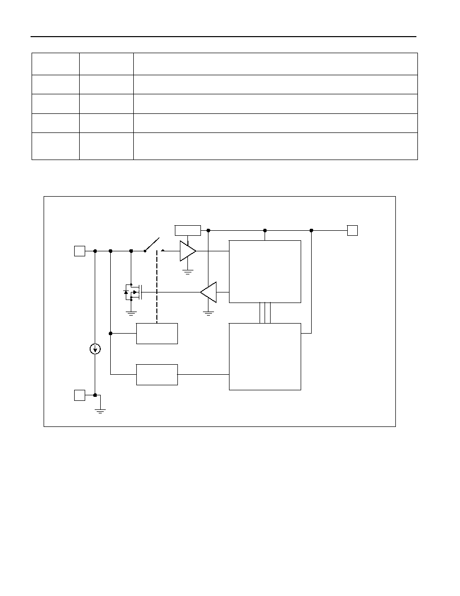
PIN DESCRIPTION
PIN NAME
FUNCTION
1, 3
N.C.
No Connection
2
V
SS
Supply GND and Reference for Serial Communication. Attach
V
SS
to battery-pack negative
terminal.
4
V
DD
Supply Input. Bypass to
V
SS
with 0.01
mF (typ).
5 DQ
Serial Interface Data I/O Pin. Bidirectional data transmit and receive at 16kbps. Input for
programming voltage pulse during EPROM programming. Internal 0.5
mA pulldown ensures
idle mode is entered when no DQ pullup is present.
Figure 1. Block Diagram
DQ
VSS
HV Shaper
1-Wire I/F
and
Control
EPROM Array
Reg.
Vdd_int
VDD
DOUT
DIN
Vpp
HV Detect
HV
0.5
mA
DETAILED DESCRIPTION
The DS25LV02 provides battery-pack identification and data storage. A 128-byte EPROM memory array and an 8
byte status field accessed by a low-voltage 1-Wire interface. Each DS25LV02 has a unique 64-bit Net Address
(ROM ID) for identification.
The EPROM is divided into four 32-byte pages. An additional 8-byte status field provides lock bit and page
redirection information to the user. EPROM writing occurs one byte at a time by supplying a 12V pulse on the DQ
line in-between each byte written. Each page can be individually locked by clearing the appropriate bit in the Status
field. Data is read sequentially from a starting address through the end of the array. CRC verification provides
integrity of all read and written data.
Functional compatibility has been maintained between the DS2502 and DS25LV02 at the Net Address/ROM
Command and Function Command levels for reading and writing the Memory data and Status data fields.

DS25LV02: Low-Voltage 1024-Bit EPROM
5 of 17
EPROM MEMORY DATA FIELD
The DS25LV02 has a linear address space for access to the EPROM data field. The EPROM data field is
organized as 4 pages of 32 bytes each as shown in Table 1. The Read Memory and Read Data/Generate CRC
Memory function commands provide read access to the 1024 bits of the EPROM data field. The Write Memory
function command provides write access to the EPROM data field. When received from the factory, the entire
1024-bit EPROM data field is erased and returns logical 1's when read. Bits within the data field are one time
programmable. Programming changes the bit value to logical zero from the factory default erased value of a logical
1. Once a bit is programmed, it cannot be set back to a logical 1.
Table 1. EPROM Data Field
ADDRESS (HEX)
DESCRIPTION
READ/WRITE
0000001F
PAGE 0 (32 bytes)
R/W*
0020003F
PAGE 1 (32 bytes)
R/W*
0040005F
PAGE 2 (32 bytes)
R/W*
0060007F
PAGE 3 (32 bytes)
R/W*
0080FFFF
Reserved
* One-time write to "0" for each bit.
READ MEMORY [F0h]
The Read Memory command is used to read data from PAGE 0 to PAGE 3 of the 1024-bit EPROM data field. The
bus master follows the command byte with a 2-byte address (TA1 = (T7:T0), TA2 = (T15:T8)) that indicates a
starting byte location within the data field. An 8-bit CRC of the command byte and address bytes is computed by
the DS25LV02 and read back by the bus master to confirm that the correct command word and starting address
were received. If the CRC is deemed to be incorrect by the bus master, the bus master should issue a reset pulse
and repeat the entire sequence. If the CRC is deemed to be correct by the bus master, read time slots can be
issued to receive data from the EPROM data field starting at the initial address. The bus master can issue a reset
pulse at any point or continue to issue read time slots until the end of PAGE 3 of the data field is reached.
If reading continues through the end of PAGE 3, the bus master can issue eight additional read time slots and the
DS25LV02 will respond with a 8-bit CRC of all data bytes read from the initial starting byte through the last byte of
PAGE 3. Terminating the command transaction with a reset pulse prior to reaching the end of PAGE 3 results in a
loss of availability of the 8-bit CRC.
READ DATA/GENERATE 8-BIT CRC [C3h]
The Read Data/Generate 8-bit CRC command is used to read data from PAGE 0 to PAGE 3 of the 1024-bit
EPROM data field. The bus master follows the command byte with a 2-byte address
(TA1 = (T7:T0), TA2 = (T15:T8)) that indicates a starting byte location within the data field. An 8-bit CRC of the
command byte and address bytes is computed by the DS25LV02 and read back by the bus master to confirm that
the correct command word and starting address were received. If the CRC is deemed to be incorrect by the bus
master, the bus master should issue a reset pulse and repeat the entire sequence. If the CRC is deemed to be
correct by the bus master, read time slots can be issued to receive data from the EPROM data field starting at the
initial address. The bus master can issue a reset pulse at any point or continue to issue read time slots until the
end of the 32-byte page is reached. If reading occurs through the end of the 32-byte page, the bus master can
issue eight additional read time slots and the DS25LV02 will respond with an 8-bit CRC of all data bytes read from
the initial starting byte through the last byte of the current page. After the CRC is received, additional read time
slots return data starting with the first byte of the next page. This sequence will continue until the bus master reads
PAGE 3 and its accompanying CRC. Thus each page of data can be considered to be 33 bytes long: the 32 bytes
of user-programmed EPROM data and an 8-bit CRC that gets generated automatically at the end of each page.
The Read Data/Generate 8-Bit CRC command sequence can be exited at any point by issuing a reset pulse.