 | ÐлекÑÑоннÑй компоненÑ: DS26102 | СкаÑаÑÑ:  PDF PDF  ZIP ZIP |
FEATURES
1 of 64
REV: 021403
Note: Some revisions of this device may incorporate deviations from published specifications known as errata. Multiple revisions of any device
may be simultaneously available through various sales channels. For information about device errata, click here:
www.maxim-ic.com/errata
.
GENERAL DESCRIPTION
On the transmit side, the DS26102 receives ATM cells
from an ATM device through a UTOPIA II interface,
provides cell buffering (up to 4 cells), HEC generation
and insertion, cell scrambling, and converts the data
to a serial stream appropriate for interfacing to a
T1/E1 framer or transceiver. On the receive side, the
DS26102 receives a TDM stream from a T1/E1 framer
or transceiver; searches for the cell alignment; verifies
the HEC; provides cell filtering, descrambling, and cell
buffering; and passes the cells to an ATM device
through the UTOPIA II interface. Other low-level traffic
management functions are selectable for the transmit
and receive paths. The DS26102 can also be used in
fractional T1/E1 applications.
The DS26102 maps ATM cells to T1/E1 TDM frames
as per the ATM Forum Specifications af-phy-0016.000
and af-phy-0064.000. In the receive direction, the cell
delineation mechanism used for finding ATM cell
boundary within T1/E1 frame is performed as per ITU
I.432. The DS26102 provides a mapping solution for
up to 16 T1/E1 TDM ports. The terms physical layer
(PHY) and line side are used synonymously in this
document and refer to the device interfacing with the
line side of the DS26102. The terms ATM layer and
system side are used synonymously and refer to the
DS26102's UTOPIA II interface.
FUNCTIONAL DIAGRAM
FEATURES
§ Supports 16 T1/E1 TDM Ports
§ Supports Fractional T1/E1
§ Compliant to ATM Forum Specifications for ATM
Over T1 and E1
§ Standard UTOPIA II Interface to the ATM Layer
§ Configurable UTOPIA Address Range
§ Configurable Tx FIFO Depth to 2, 3, or 4 Cells
§ Optional Payload Scrambling in Transmit
Direction and Descrambling in Receive Direction
per ITU I.432
§ Optional HEC Insertion in Transmit Direction with
Programmable COSET Polynomial Addition
§ HEC-Based Cell Delineation
§ Single-Bit HEC Error Correction in the Receive
Direction
§ Receive HEC-Errored Cell Filtering
§ Receive Idle/Unassigned Cell Filtering
§ User-Definable Cell Filtering
§ 8-Bit Mux/Nonmux, Motorola/Intel Microprocessor
Interface
§ Internal Clock Generator Eliminates External
High-Speed Clocks
§ Internal One-Second Timer
§ Detects/Reports Up to Eight External Status
Signals with Interrupt Support
§ IEEE 1149.1 JTAG Boundary Scan Support
§
17mm x 17mm, 256-Pin CSBGA
Features continued on page 5.
APPLICATIONS
DSLAMS
ATM Over T1/E1
Routers
IMA
ORDERING INFORMATION
PART TEMP
RANGE
PIN-PACKAGE
DS26102
-40°C to +85°C
256 CSBGA
www.maxim-ic.com
DS26102
16-Port TDM-to-ATM PHY
UTOPIA II
16 TDM
PORTS
DS26102

DS26102 16-Port TDM-to-ATM PHY
2 of 64
TABLE OF CONTENTS
1.
FEATURES ......................................................................................................................................5
2.
APPLICABLE STANDARDS............................................................................................................5
3.
ACRONYMS AND DEFINITIONS.....................................................................................................6
4.
BLOCK DIAGRAM ...........................................................................................................................7
5.
PIN DESCRIPTION ..........................................................................................................................8
6.
SIGNAL DEFINITIONS...................................................................................................................12
6.1
TDM S
IGNALS
..........................................................................................................................12
6.2
UTOPIA-S
IDE
S
IGNALS
............................................................................................................12
6.3
M
ICROPROCESSOR AND
S
YSTEM
I
NTERFACE
S
IGNALS
................................................................14
6.4
T
EST AND
JTAG S
IGNALS
.........................................................................................................16
7.
TRANSMIT OPERATION ...............................................................................................................17
7.1
UTOPIA-S
IDE
T
RANSMIT
--M
UXED
M
ODE WITH
1 TXCLAV ........................................................17
7.2
UTOPIA-S
IDE
T
RANSMIT
--D
IRECT
S
TATUS
M
ODE
(MULTITXCLAV) .........................................19
7.3
T
RANSMIT
P
ROCESSING
............................................................................................................20
7.4
P
HYSICAL
-S
IDE
T
RANSMIT
.........................................................................................................21
8.
RECEIVE OPERATION..................................................................................................................23
8.1
P
HYSICAL
-S
IDE
R
ECEIVE
...........................................................................................................23
8.2
R
ECEIVE
P
ROCESSING
..............................................................................................................25
8.3
UTOPIA-S
IDE
R
ECEIVE
--M
UXED
M
ODE WITH
1 RXCLAV..........................................................27
8.4
UTOPIA-S
IDE
R
ECEIVE
--D
IRECT
S
TATUS
M
ODE
(MULTIRXCLAV) ...........................................28
9.
REGISTER MAPPING....................................................................................................................30
10.
REGISTER DEFINITIONS..............................................................................................................31
10.1
T
RANSMIT
R
EGISTERS
..............................................................................................................31
10.2
S
TATUS
R
EGISTERS
..................................................................................................................35
10.3
R
ECEIVE
R
EGISTERS
................................................................................................................36
11.
JTAG BOUNDARY SCAN ARCHITECTURE AND TEST ACCESS PORT....................................45
11.1
I
NSTRUCTION
R
EGISTER
............................................................................................................48
11.2
T
EST
R
EGISTERS
......................................................................................................................49
12.
OPERATING PARAMETERS.........................................................................................................52
13.
CRITICAL TIMING INFORMATION................................................................................................53
14.
THERMAL INFORMATION ............................................................................................................59
15.
APPLICATIONS INFORMATION ...................................................................................................60
15.1
A
PPLICATION IN
ATM U
SER
-N
ETWORK
I
NTERFACES
...................................................................60
15.2
I
NTERFACING WITH
F
RAMERS
....................................................................................................60
15.3
F
RACTIONAL
T1/E1 S
UPPORT
...................................................................................................61
16.
PACKAGE INFORMATION............................................................................................................62
17.
REVISION HISTORY......................................................................................................................64

DS26102 16-Port TDM-to-ATM PHY
3 of 64
TABLE OF FIGURES
Figure 4-1. Block Diagram ....................................................................................................................... 7
Figure 7-1. Polling Phase and Selection Phase at Transmit Interface.....................................................18
Figure 7-2. End and Restart of Cell at Transmit Interface .......................................................................18
Figure 7-3. Transmission to PHY Paused for Three Cycles ....................................................................19
Figure 7-4. Example of Direct Status Indication, Transmit Direction .......................................................20
Figure 7-5. Transmit Cell Flow and Processing ......................................................................................21
Figure 7-6. Transmit Framer Interface in TFP Mode for T1.....................................................................22
Figure 7-7. Transmit Framer Interface in Gapped-Clock Mode for T1.....................................................22
Figure 7-8. Transmit Framer Interface in TFP Mode for E1.....................................................................22
Figure 7-9. Transmit Framer Interface in Gapped-Clock Mode for E1.....................................................23
Figure 8-1. Receive Framer Interface in RFP Mode for T1 .....................................................................24
Figure 8-2. Receive Framer Interface in Gapped-Clock Mode for T1......................................................24
Figure 8-3. Receive Framer Interface in RFP Mode for E1 .....................................................................25
Figure 8-4. Receive Framer Interface in Gapped-Clock Mode for E1......................................................25
Figure 8-5. Cell Delineation State Diagram.............................................................................................26
Figure 8-6. Header Correction State Machine.........................................................................................26
Figure 8-7. Polling Phase and Selection at Receive Interface.................................................................27
Figure 8-8. End and Restart of Cell Transmission at Receive Interface ..................................................28
Figure 8-9. Example Direct Status Indication, Receive Direction ............................................................29
Figure 10-1. Accessing Tx PMON Counter.............................................................................................34
Figure 10-2. Accessing Rx PMON Counters...........................................................................................40
Figure 11-1. JTAG Functional Block Diagram.........................................................................................45
Figure 11-2. TAP Controller State Diagram ............................................................................................47
Figure 13-1. Intel Bus Read Timing (BTS = 0/MUX = 1) .........................................................................53
Figure 13-2. Intel Bus Write Timing (BTS = 0/MUX = 1) .........................................................................54
Figure 13-3. Motorola Bus Timing (BTS = 1/MUX = 1)............................................................................54
Figure 13-4. Intel Bus Read Timing (BTS = 0/MUX = 0) .........................................................................55
Figure 13-5. Intel Bus Write Timing (BTS = 0/MUX = 0) .........................................................................56
Figure 13-6. Motorola Bus Read Timing (BTS = 1/MUX = 0) ..................................................................56
Figure 13-7. Motorola Bus Write Timing (BTS = 1/MUX = 0) ..................................................................56
Figure 13-8. Setup/Hold Time Definition .................................................................................................58
Figure 13-9. Delay Time Definition .........................................................................................................58
Figure 13-10. JTAG Interface Timing Diagram .......................................................................................58
Figure 15-1. User-Network Interface Application ....................................................................................60
Figure 15-2. DS26102 Interfacing with Dallas Framer in Framing-Pulse Mode .......................................61

DS26102 16-Port TDM-to-ATM PHY
4 of 64
LIST OF TABLES
Table 5-A. Pin Description List ................................................................................................................ 8
Table 9-A. Register Map.........................................................................................................................30
Table 11-A. Instruction Codes for IEEE 1149.1 Architecture...................................................................48
Table 11-B. ID Code Structure ...............................................................................................................48
Table 11-C. Device ID Codes .................................................................................................................48
Table 11-D. Boundary Scan Control Bits ................................................................................................49
Table 13-A. AC Characteristics--Multiplexed Parallel Port (MUX = 1)....................................................53
Table 13-B. AC Characteristics--Nonmultiplexed Parallel Port (MUX = 1) .............................................55
Table 13-C. Framer Interface AC Characteristics ...................................................................................57
Table 13-D. UTOPIA Transmit AC Characteristics .................................................................................57
Table 13-E. UTOPIA Receive AC Characteristics...................................................................................57
Table 13-F. JTAG Interface Timing.........................................................................................................58
Table 13-G. System Clock AC Characteristics........................................................................................59
Table 14-A. Thermal Properties, Natural Convection..............................................................................59
Table 14-B. Theta-JA (
q
JA
) vs. Airflow.....................................................................................................59
Table 15-A. Suggested Clock Edge Configurations ................................................................................61
Table 15-B. Fractional T1/E1 Register Settings ......................................................................................61

DS26102 16-Port TDM-to-ATM PHY
5 of 64
1. FEATURES
§
Supports 16 T1/E1 Ports
§
Supports Fractional T1/E1 and Arbitrary Bit
Rates in Multiples of 64kbps (DS0/TS) Up to
2.048Mbps
§
Supports Clear E1
§
Compliant to the ATM Forum Specifications for
ATM Over T1 and E1
§
Standard UTOPIA II Interface to the ATM Layer
§
Configurable UTOPIA Address Range
§
Generic 8-Bit Asynchronous Microprocessor
Interface for Configuration and Status Indications
Including Interrupt Capability
§
Physical Layer Interface Can Accept T1/E1 TDM
Stream in the Form of Either (1) Clock, Data, and
Frame-Overhead Indication or (2) Gapped Clock
(Gapped at Overhead Positions in the Frame)
and Data
§
Selectable Active Clock Edge for Interface with
the T1/E1 Framer
§
Supports Diagnostic Loopback
§
Optional Payload Scrambling in Transmit
Direction and Descrambling in Receive Direction
as per the ITU I.432 for the Cell-Based Physical
Layer
§
Optional HEC Insertion in Transmit Direction with
Programmable COSET Polynomial Addition
§
Option of Using Either Idle or Unassigned Cells
for Cell-Rate Decoupling in Transmit Direction
§
1-Byte Programmable Pattern for Payload of
Cells Used for Cell-Rate Decoupling
§
Tx FIFO Depth Configurable to Either 2, 3, or 4
Cells
§
Transmit FIFO Depth Indication for 2-Cell Space
Through External Pins
§
Optional Single-Bit HEC Error Insertion
§
HEC-Based Cell Delineation as per I.432
§
Optional Single-Bit HEC Error Correction in the
Receive Direction
§
Optional Filtering of HEC-Errored Cells Received
§
Optional Receive Idle/Unassigned Cell Filtering
§
Optional User-Defined Cell Filtering Based on
Programmable Header Bits
§
Programmable Loss-Of-Cell Delineation (LCD)
Integration and Interrupt
§
Interrupt for FIFO Overrun in Receive Direction
§
Saturating Counts for (1) Number of Error-Free
Assigned Cells Received and Transmitted and
(2) Number of Correctable and Uncorrectable
HEC-Errored Cells Received
§
Selectable Internally Generated Clock (System
Clock Divided by 8) in Diagnostic Loopback
Mode
§
Integrated PLL Generates High-Frequency
Clocks
§
IEEE 1149.1 JTAG Boundary Scan Support
2. APPLICABLE STANDARDS
[1] ATM Forum "DS1 Physical Layer Specification," af-phy-0016.000, September 1994
[2] ATM Forum "E1 Physical Layer Specification," af-phy-0064.000, September 1996
[3] ATM Forum "UTOPIA Level 2 Specification," Version 1.0, af-phy-0039.000, June 1995
[4] B-ISDN User-Network Interface--Physical Layer Specification--ITU-T Recommendation I.432--3/93

DS26102 16-Port TDM-to-ATM PHY
6 of 64
3. ACRONYMS AND DEFINITIONS
ACRONYM DESCRIPTION
ATM
Asynchronous Transfer Mode
CRC Cyclic
Redundancy
Check
DPRAM
Dual Port Random Access Memory
FIFO
First In, First Out (Memory)
HEC
Header Error Check
IMA
Inverse Multiplexing for ATM
µP Microprocessor
µs Microsecond
LCD Loss-of-Cell
Delineation
ms Millisecond
OAM
Operations Administration and Maintenance
OCD Out-of-Loss
Delineation
PMON Performance
Monitoring
Rx Receive
DS0
Each 64kbps Channel in DS1 Frame
TS
Each 64kbps Channel in E1 Frame (Time Slot)
Tx Transmit
UTOPIA
Universal Test and Operations PHY Interface for ATM
DS26102 16-Port TDM-to-ATM PHY
7 of 64
4. BLOCK DIAGRAM
Figure 4-1. Block Diagram
TRANSMIT
TDM
INTERFACE
CONTROL
SCRAMBLING
AND RATE
DECOUPLING
CELL
STORAGE
FIFO
TRANSMIT
UTOPIA BUS
INTERFACE
RECEIVE
TDM
INTERFACE
CONTROL
SCRAMBLING
AND RATE
DECOUPLING
CELL
STORAGE
FIFO
RECEIVE
UTOPIA BUS
INTERFACE
RCLK015
RDATA015
RFP015
TCLK015
TDATA015
TFP015
16
16
16
16
16
16
DS26102
CONTROLLER INTERFACE
JTAG
A
0A
6
A
D0A
D7
JT
C
L
K
JT
D
O
JT
D
I
JT
M
S
JT
R
S
T
8
7
A
7
/
AL
E (
A
S)
C
S
R
D
(
DS
)
W
R
(
R/
W
)
BTS
MU
X
I
NT
R
ESET
RLCD0-15
16
UR-SOC
UR-CLK
UR-ADDR04
UR-DATA07
UR-CLAV03
5
8
UR-PAR
4
UR-ENB
UT-SOC
UT-CLK
UT-ADDR04
UT-DATA07
UT-CLAV0 3
5
8
UT-2CLAV0 3
UT_PAR
4
4
UT-ENB
REFCLKIN
GCLKOUT
GCLKIN
TEST
CLOCK
PLL
EX
STA
T
0
-
7
8
8KHZIN
1SECOUT
1-SECOND
TIMER
BL
S0

DS26102 16-Port TDM-to-ATM PHY
8 of 64
5. PIN DESCRIPTION
Table 5-A. Pin Description List
PIN NAME
I/O FUNCTION
J13 1SECOUT
O
One-Second
Reference
J12
8KHZIN
I
8kHz Clock for One-Second Timer
F16
A0
I
µP Address Bus Bit 0
F13
A1
I
µP Address Bus Bit 1
F12
A2
I
µP Address Bus Bit 2
G15
A3
I
µP Address Bus Bit 3
G14
A4
I
µP Address Bus Bit 4
G16
A5
I
µP Address Bus Bit 5
G13
A6
I
µP Address Bus Bit 6
G12
A7/ALE (AS)
I
µP Address Bus Bit 7 (Note 1)
C14 BLS0
I
Block
Select
0
C16
BTS
I
Bus Type Select (0 = Intel)
D14
CS
I
Chip Select (Active Low)
D16
D0/AD0
I/O
µP Data 0/Address/Data 0
E15
D1/AD1
I/O
µP Data 1/Address/Data 1
E14
D2/AD2
I/O
µP Data 2/Address/Data 2
E16
D3/AD3
I/O
µP Data 3/Address/Data 3
E13
D4/AD4
I/O
µP Data 4/Address/Data 4
E12
D5/AD5
I/O
µP Data 5/Address/Data 5
F15
D6/AD6
I/O
µP Data 6/Address/Data 6
F14
D7/AD7
I/O
µP Data 7/Address/Data 7
J16
EXSTAT0
I
External Status Input
J14
EXSTAT1
I
External Status Input
J15
EXSTAT2
I
External Status Input
H12
EXSTAT3
I
External Status Input
H13
EXSTAT4
I
External Status Input
H16
EXSTAT5
I
External Status Input
H14
EXSTAT6
I
External Status Input
H15
EXSTAT7
I
External Status Input
K13
GCLKIN
I
High-Frequency Clock Input
K12
GCLKOUT
O
High-Frequency Clock Output
B16
INT
O
Interrupt Signal (Active Low) (Note 2)
P16
JTCLK
I
IEEE 1149.1 Test Clock
N16
JTDI
I
IEEE 1149.1 Test Data Input
N15
JTDO
O
IEEE 1149.1 Test Data Output
P15
JTMS
I
IEEE 1149.1 Test Mode Select
N14
JTRST
I
IEEE 1149.1 Reset
C15
MUX
I
Bus Mode Select (0 = Nonmuxed)
A1, A15, A16, B1, B2, B15,
C1, C2, L16, P3, R1, R2,
R15, R16, T1, T2, T16
N.C. --
No
Connect
A14
RCLK0
I
Rx Line Clock for Port 0
B13
RCLK1
I
Rx Line Clock for Port 1
N8
RCLK11
I
Rx Line Clock for Port 11
P7
RCLK10
I
Rx Line Clock for Port 10
R8
RCLK12
I
Rx Line Clock for Port 12
T9
RCLK13
I
Rx Line Clock for Port 13
M10
RCLK14
I
Rx Line Clock for Port 14
P10
RCLK15
I
Rx Line Clock for Port 15
C12
RCLK2
I
Rx Line Clock for Port 2
D11
RCLK3
I
Rx Line Clock for Port 3
B11
RCLK4
I
Rx Line Clock for Port 4
A10
RCLK5
I
Rx Line Clock for Port 5
E9
RCLK6
I
Rx Line Clock for Port 6
C9
RCLK7
I
Rx Line Clock for Port 7

DS26102 16-Port TDM-to-ATM PHY
9 of 64
PIN NAME
I/O FUNCTION
T6
RCLK8
I
Rx Line Clock for Port 8
M7
RCLK9
I
Rx Line Clock for Port 9
D15
RD (DS)
I
Read Enable (Active Low)
B14
RDATA0
I
Rx Line Serial Data for Port 0
A13
RDATA1
I
Rx Line Serial Data for Port 1
T7
RDATA10
I
Rx Line Serial Data for Port 10
M8
RDATA11
I
Rx Line Serial Data for Port 11
P8
RDATA12
I
Rx Line Serial Data for Port 12
N9
RDATA13
I
Rx Line Serial Data for Port 13
R9
RDATA14
I
Rx Line Serial Data for Port 14
T10
RDATA15
I
Rx Line Serial Data for Port 15
A12
RDATA2
I
Rx Line Serial Data for Port 2
E11
RDATA3
I
Rx Line Serial Data for Port 3
C11
RDATA4
I
Rx Line Serial Data for Port 4
D10
RDATA5
I
Rx Line Serial Data for Port 5
B10
RDATA6
I
Rx Line Serial Data for Port 6
A9
RDATA7
I
Rx Line Serial Data for Port 7
N6
RDATA8
I
Rx Line Serial Data for Port 8
R6
RDATA9
I
Rx Line Serial Data for Port 9
L15
REFCLKIN
I
1.544MHz/2.048MHz Reference Clock
L14
RESET
I
Device Reset (Active Low)
C13
RFP0
I
Rx Frame Pulse for Port 0
D12
RFP1
I
Rx Frame Pulse for Port 1
R7
RFP10
I
Rx Frame Pulse for Port 10
T8
RFP11
I
Rx Frame Pulse for Port 11
M9
RFP12
I
Rx Frame Pulse for Port 12
P9
RFP13
I
Rx Frame Pulse for Port 13
N10
RFP14
I
Rx Frame Pulse for Port 14
R10
RFP15
I
Rx Frame Pulse for Port 15
B12
RFP2
I
Rx Frame Pulse for Port 2
A11
RFP3
I
Rx Frame Pulse for Port 3
E10
RFP4
I
Rx Frame Pulse for Port 4
C10
RFP5
I
Rx Frame Pulse for Port 5
D9
RFP6
I
Rx Frame Pulse for Port 6
B9
RFP7
I
Rx Frame Pulse for Port 7
P6
RFP8
I
Rx Frame Pulse for Port 8
N7
RFP9
I
Rx Frame Pulse for Port 9
N1
RLCD0
O
Rx Loss-of-Cell Delineation Port 0
N2
RLCD1
O
Rx Loss-of-Cell Delineation Port 1
R4
RLCD10
O
Rx Loss-of-Cell Delineation Port 10
N5
RLCD11
O
Rx Loss-of-Cell Delineation Port 11
T5
RLCD12
O
Rx Loss-of-Cell Delineation Port 12
P5
RLCD13
O
Rx Loss-of-Cell Delineation Port 13
R5
RLCD14
O
Rx Loss-of-Cell Delineation Port 14
M6
RLCD15
O
Rx Loss-of-Cell Delineation Port 15
N4
RLCD2
O
Rx Loss-of-Cell Delineation Port 2
N3
RLCD3
O
Rx Loss-of-Cell Delineation Port 3
P1
RLCD4
O
Rx Loss-of-Cell Delineation Port 4
P2
RLCD5
O
Rx Loss-of-Cell Delineation Port 5
R3
RLCD6
O
Rx Loss-of-Cell Delineation Port 6
T3
RLCD7
O
Rx Loss-of-Cell Delineation Port 7
P4
RLCD8
O
Rx Loss-of-Cell Delineation Port 8
T4
RLCD9
O
Rx Loss-of-Cell Delineation Port 9
J3
UR_ADDR0
I
Rx UTOPIA Address 0 (LSB)
J1
UR_ADDR1
I
Rx UTOPIA Address 1
J4
UR_ADDR2
I
Rx UTOPIA Address 2
J5
UR_ADDR3
I
Rx UTOPIA Address 3
H2
UR_ADDR4
I
Rx UTOPIA Address 4 (MSB)

DS26102 16-Port TDM-to-ATM PHY
10 of 64
PIN NAME
I/O FUNCTION
M5
UR_CLAV0
O
Rx UTOPIA Cell Available 0
M4
UR_CLAV1
O
Rx UTOPIA Cell Available 1
M1
UR_CLAV2
O
Rx UTOPIA Cell Available 2
M3
UR_CLAV3
O
Rx UTOPIA Cell Available 3
K5
UR_CLK
I
Rx UTOPIA Clock
L3
UR_DATA0
O
Rx UTOPIA Data Bus 0 (LSB)
L1
UR_DATA1
O
Rx UTOPIA Data Bus 1
L4
UR_DATA2
O
Rx UTOPIA Data Bus 2
L5
UR_DATA3
O
Rx UTOPIA Data Bus 3
K2
UR_DATA4
O
Rx UTOPIA Data Bus 4
K3
UR_DATA5
O
Rx UTOPIA Data Bus 5
K1
UR_DATA6
O
Rx UTOPIA Data Bus 6
K4
UR_DATA7
O
Rx UTOPIA Data Bus 7 (MSB)
J2
UR_ENB
I
Rx UTOPIA Enable (Active Low)
M2
UR_PAR
O
Rx UTOPIA Parity Bit
L2
UR_SOC
O
Rx UTOPIA Start of Cell
D8
TCLK0
I
Tx Line Clock for Port 0
B8
TCLK1
I
Tx Line Clock for Port 1
T12
TCLK10
I
Tx Line Clock for Port 10
T13
TCLK11
I
Tx Line Clock for Port 11
P13
TCLK12
I
Tx Line Clock for Port 12
P14
TCLK13
I
Tx Line Clock for Port 13
M16
TCLK14
I
Tx Line Clock for Port 14
L12
TCLK15
I
Tx Line Clock for Port 15
A7
TCLK2
I
Tx Line Clock for Port 2
E6
TCLK3
I
Tx Line Clock for Port 3
C6
TCLK4
I
Tx Line Clock for Port 4
D5
TCLK5
I
Tx Line Clock for Port 5
B5
TCLK6
I
Tx Line Clock for Port 6
D4
TCLK7
I
Tx Line Clock for Port 7
N11
TCLK8
I
Tx Line Clock for Port 8
R11
TCLK9
I
Tx Line Clock for Port 9
E8
TDATA0
O
Tx Line Serial Data for Port 0
C8
TDATA1
O
Tx Line Serial Data for Port 1
N12
TDATA10
O
Tx Line Serial Data for Port 10
R12
TDATA11
O
Tx Line Serial Data for Port 11
N13
TDATA12
O
Tx Line Serial Data for Port 12
R14
TDATA13
O
Tx Line Serial Data for Port 13
M13
TDATA14
O
Tx Line Serial Data for Port 14
M15
TDATA15
O
Tx Line Serial Data for Port 15
D7
TDATA2
O
Tx Line Serial Data for Port 2
B7
TDATA3
O
Tx Line Serial Data for Port 3
A6
TDATA4
O
Tx Line Serial Data for Port 4
E5
TDATA5
O
Tx Line Serial Data for Port 5
C5
TDATA6
O
Tx Line Serial Data for Port 6
B4
TDATA7
O
Tx Line Serial Data for Port 7
M11
TDATA8
O
Tx Line Serial Data for Port 8
P11
TDATA9
O
Tx Line Serial Data for Port 9
K16 TEST
I
Test
Control
A8
TFP0
I/O
Tx Frame Pulse for Port 0
E7 TFP1
I/O
Tx Frame Pulse for Port 1
P12 TFP10
I/O
Tx Frame Pulse for Port 10
R13 TFP11
I/O
Tx Frame Pulse for Port 11
T14 TFP12
I/O
Tx Frame Pulse for Port 12
T15 TFP13
I/O
Tx Frame Pulse for Port 13
M14 TFP14
I/O
Tx Frame Pulse for Port 14
L13 TFP15
I/O
Tx Frame Pulse for Port 15
C7 TFP2
I/O
Tx Frame Pulse for Port 2

DS26102 16-Port TDM-to-ATM PHY
11 of 64
PIN NAME
I/O FUNCTION
D6 TFP3
I/O
Tx Frame Pulse for Port 3
B6 TFP4
I/O
Tx Frame Pulse for Port 4
A5 TFP5
I/O
Tx Frame Pulse for Port 5
A4 TFP6
I/O
Tx Frame Pulse for Port 6
C4 TFP7
I/O
Tx Frame Pulse for Port 7
T11 TFP8
I/O
Tx Frame Pulse for Port 8
M12 TFP9
I/O
Tx Frame Pulse for Port 9
G1
UT_2CLAV0
O
Tx UTOPIA 2 Cells Available 0
H4
UT_2CLAV1
O
Tx UTOPIA 2 Cells Available 1
H1
UT_2CLAV2
O
Tx UTOPIA 2 Cells Available 2
H3
UT_2CLAV3
O
Tx UTOPIA 2 Cells Available 3
D3
UT_ADDR0
I
Tx UTOPIA Address 0 (LSB)
A2
UT_ADDR1
I
Tx UTOPIA Address 1
C3
UT_ADDR2
I
Tx UTOPIA Address 2
B3
UT_ADDR3
I
Tx UTOPIA Address 3
A3
UT_ADDR4
I
Tx UTOPIA Address 4 (MSB)
G4
UT_CLAV0
O
Tx UTOPIA Cell Available 0
G3
UT_CLAV1
O
Tx UTOPIA Cell Available 1
G2
UT_CLAV2
O
Tx UTOPIA Cell Available 2
H5
UT_CLAV3
O
Tx UTOPIA Cell Available 3
F2
UT_CLK
I
Tx UTOPIA Clock
F1
UT_DATA0
I
Tx UTOPIA Data Bus 0 (LSB)
F4
UT_DATA1
I
Tx UTOPIA Data Bus 1
F5
UT_DATA2
I
Tx UTOPIA Data Bus 2
E2
UT_DATA3
I
Tx UTOPIA Data Bus 3
E3
UT_DATA4
I
Tx UTOPIA Data Bus 4
E1
UT_DATA5
I
Tx UTOPIA Data Bus 5
E4
UT_DATA6
I
Tx UTOPIA Data Bus 6
D2
UT_DATA7
I
Tx UTOPIA Data Bus 7 (MSB)
D1
UT_ENB
I
Tx UTOPIA Enable (Active Low)
G5
UT_PAR
I
Tx UTOPIA Parity Bit
F3
UT_SOC
I
Tx UTOPIA Start of Cell
F8, F9, G8, G9, H6, H7,
H10, H11, J6, J7, J10, J11,
K8, K9, L8, L9
VDD --
Positive
Supply
F6, F7, F10, F11, G6, G7,
G10, G11, H8, H9, J8, J9,
K6, K7, K10, K11, K14,
K15, L6, L7, L10, L11
VSS --
Ground
D13
WR (R/W)
I
Write Enable (Active Low)
Note 1: Address-latch enable for muxed bus.
Note 2: Open-drain output.

DS26102 16-Port TDM-to-ATM PHY
12 of 64
6. SIGNAL DEFINITIONS
6.1 TDM
Signals
Signal Name:
RCLK015
Signal Description:
Receive Line Clock (Ports 0 to 15)
Signal Type:
Input
The physical layer device uses the RCLK input to latch the RDATA and RFP signals. RDATA and RFP are sampled
by the receive section of the DS26102 at either the positive edge or negative edge of RCLK, as controlled by the
RAES (RCR2.2) control bit. RCLK is gapped during nonactive and framing bit positions in gapped-clock mode
(RPLIM = 1). RCLK should be glitch-free.
Signal Name:
RDATA015
Signal Description:
Receive Line Data (Ports 0 to 15)
Signal Type:
Input
The RDATA input carries the receive bit stream. If the RCLK is gapped at framing bit positions, RDATA is then
sampled at every RCLK tick. If RCLK is not gapped and RFP is used to indicate framing bit positions, the RDATA
bits that are not associated with framing-overhead bits are sampled and cell delineated. In clear E1, RDATA is
sampled at every RCLK tick.
Signal Name:
RFP015
Signal Description:
Receive Frame Pulse (Ports 0 to 15)
Signal Type:
Input
This active-high signal indicates the framing-overhead bit positions corresponding to RDATA. For T1/E1, this aligns
with the first bit of the T1/E1 frame. For T1, RDATA coming at the RFP position is ignored. For E1, RFP is used to
identify TS0 (RFP position is bit 0 of TS0) and TS16 locations, and RDATA coming at these slots are ignored. In
clear E1, RFP is ignored. In frame-pulse mode, the RFP should come once every 125
ms.
Signal Name:
TCLK015
Signal Description:
Transmit Line Clock (Ports 0 to 15)
Signal Type:
Input
The TCLK input is used by the DS26102's transmit section to launch TDATA and TFP (when configured as an
output) at either positive edge or negative edge, as controlled by the TAES (TCR2.2) control bit.
Signal Name:
TDATA015
Signal Description:
Transmit Line Data (Ports 0 to 15)
Signal Type:
Output
The TDATA output carries the transmit bit stream. ATM layer data bits are not transmitted during framing/overhead
bit locations. TDATA is output at the TCLK configured active edge.
Signal Name:
TFP015
Signal Description:
Transmit Frame Pulse (Ports 0 to 15)
Signal Type:
Input/Output
This active-high signal can be set as an input or an output by using the TFSD (TCR2.0) control bit. TFP indicates
the frame-overhead bit positions corresponding to TDATA. For T1/E1, this signal aligns with the first bit of the
T1/E1 frame. For T1, TDATA coming at the TFP position does not contain valid data bit. For E1, TFP is used to
identify TS0 (TFP position is bit 0 of TS0) and TS16. TDATA does not contain valid data at these locations. After
RESET, the DS26102 is configured to use this signal as an input. In frame-pulse mode, the TFP should occur once
every 125
ms.
6.2 UTOPIA-Side
Signals
Signal Name:
UR_CLK
Signal Description:
Receive UTOPIA Clock
Signal Type:
Input
This clock is used to register and control all other UTOPIA signals on the receive side.

DS26102 16-Port TDM-to-ATM PHY
13 of 64
Signal Name:
UR_ADDR[4:0]
Signal Description:
Receive UTOPIA Address
Signal Type:
Input
The ATM layer drives this 5-bit UTOPIA address bus to select the appropriate UTOPIA port. UR_ADDR4 is the
MSB and UR_ADDR0 is the LSB.
Signal Name:
UR_ENB
Signal Description:
Receive UTOPIA Enable
Signal Type:
Input
The ATM layer asserts this active-low signal to indicate that UR_DATA and UR_SOC are sampled at the end of the
next cycle.
Signal Name:
UR_SOC
Signal Description:
Receive UTOPIA Start of Cell
Signal Type:
Output
The DS26102 asserts this active-high, tri-statable signal when UR_DATA contains the first valid byte of a cell.
UR_SOC is enabled only in cycles following those with
UR_ENB asserted while a cell transfer is in progress.
Signal Name:
UR_DATA[7:0]
Signal Description:
Receive UTOPIA Data Bus
Signal Type:
Output
The DS26102 drives this byte-wide data bus in response to the selection of one of the UTOPIA ports by the ATM
layer for cell transfer. This bus is three-statable, and is enabled only in cycles following those that have
UR_ENB
asserted and a cell transfer in progress for a port. UR_DATA7 is the MSB and UR_DATA0 is the LSB.
Signal Name:
UR_CLAV[3:0]
Signal Description:
Receive UTOPIA Cell Available
Signal Type:
Output
The active-high UR_CLAV signals are asserted if a complete cell is available for transfer to the ATM layer for the
polled port. If UR_ADDR does not match any of the UTOPIA port addresses, this signal is tri-stated. UR_CLAV0 is
driven in multiplexed with 1 CLAV polling mode as well as direct status mode for port 1. UR_CLAV3, UR_CLAV2,
and UR_CLAV1 are driven only in direct status mode for ports 4, 3, and 2, respectively.
Signal Name:
UR_PAR
Signal Description:
Receive UTOPIA Parity Bit
Signal Type:
Output
This three-statable signal allows for parity error checking, as calculated for the 8-bits of the UR_DATA bus, and can
represent odd or even parity as determined by the receive parity select bit (RPS) in RCR1.
Signal Name:
UT_CLK
Signal Description:
Transmit UTOPIA Clock
Signal Type:
Input
This clock is used to register and control the UTOPIA signals on the transmit side.
Signal Name:
UT_ADDR[4:0]
Signal Description:
Transmit UTOPIA Address
Signal Type:
Input
The ATM layer drives this 5-bit-wide bus to poll and select the appropriate UTOPIA port. UT_ADDR4 is the MSB
and UT_ADDR0 is the LSB.
Signal Name:
UT_ENB
Signal Description:
Transmit UTOPIA Enable
Signal Type:
Input
The ATM layer asserts this active-low enable signal during cycles when UT_DATA contains valid cell data.

DS26102 16-Port TDM-to-ATM PHY
14 of 64
Signal Name:
UT_SOC
Signal Description:
Transmit UTOPIA Start of Cell
Signal Type:
Input
The ATM layer asserts this active-high signal when UT_DATA contains the first valid byte of the cell.
Signal Name:
UT_DATA[7:0]
Signal Description:
Transmit UTOPIA Data Bus
Signal Type:
Input
The ATM layer drives this byte-wide true data to one of the selected ports. UT_DATA7 is the MSB and UT_DATA0
is the LSB.
Signal Name:
UT_CLAV[3:0]
Signal Description:
Transmit UTOPIA Cell Available
Signal Type:
Output
The DS26102 asserts this active-high UT_CLAV signal if it has cell space available to accommodate a complete
cell from the ATM layer to the polled port. If UT_ADDR does not match with any one of the UTOPIA port
addresses, this signal is tri-stated. UT_CLAV0 is driven in multiplexed with 1 CLAV polling mode as well as direct
status mode for port 1. UT_CLAV3, UT_CLAV2, and UT_CLAV1 are driven only in direct status mode for ports 4,
3, and 2, respectively.
Signal Name:
UT_2CLAV[3:0]
Signal Description:
Transmit UTOPIA 2 Cells Available
Signal Type:
Output
The DS26102 asserts this active-high UT_2CLAV signal if it has cell space available to accommodate two
complete cells from the ATM layer. If UT_ADDR does not match with any one of the UTOPIA port addresses, this
signal is tri-stated. UT_2CLAV0 is driven in multiplexed with 2 CLAV polling mode as well as direct status mode for
port 1. UT_2CLAV3, UT_2CLAV2, and UT_2CLAV1 are driven only in direct status mode for ports 4, 3, and 2,
respectively.
Signal Name:
UT_PAR
Signal Description:
Transmit UTOPIA Parity Bit
Signal Type:
Input
This signal is used for parity checking as calculated for the 8 bits of the UT_DATA bus. Transmit parity errors are
reported in the port status register (PSR) at bit 6. This bit can represent odd or even parity, as determined by the
transmit parity select (TPRS) bit in TCR1.
6.3 Microprocessor and System Interface Signals
Signal Name:
A[6:0]
Signal Description:
Microprocessor Address Bus
Signal Type:
Input
This bus selects a specific register in the DS26102 during read/write access. A7 is the MSB and A0 is the LSB. A7
is also used as the address latch enable (ALE/AS) during multiplexed bus operation (MUX = 1).
Signal Name:
A7/ALE (AS)
Signal Description:
Address Latch Enable (Address Strobe) or A7
Signal Type:
Input
In nonmultiplexed bus operation (MUX = 0), the ALE serves as the upper address bit. In multiplexed bus operation
(MUX = 1), it serves to demultiplex the bus on a positive-going edge.
Signal Name:
D[7:0]/AD[7:0]
Signal Description:
Microprocessor Data Bus
Signal Type:
Input/Output
This 8-bit, bidirectional data bus is used for read/write access of the DS26102's information and control registers.
D7/AD7 is the MSB and D0/AD0 is the LSB. This bus also carries address information during multiplexed operation
(MUX = 1).

DS26102 16-Port TDM-to-ATM PHY
15 of 64
Signal Name:
CS
Signal Description:
Chip Select
Signal Type:
Input
This active-low signal is used to qualify register read/write accesses. The
RD and WR signals are qualified with CS.
Signal Name:
RD (DS)
Signal Description:
Read Enable
Signal Type:
Input
Along with CS, this active-low signal qualifies read access to one of the DS26102 registers. While
RD and CS are
both low, the DS26102 drives the D/AD bus with the contents of the addressed register.
Signal Name:
WR (R/W)
Signal Description:
Write Enable
Signal Type:
Input
Along with
CS, this active-low signal qualifies write access to one of the DS26102 registers. Data at D/AD[7:0] is
written into the addressed register at the rising edge of
WR while CS is low.
Signal Name:
INT
Signal Description:
Interrupt
Signal Type:
Output
This active-low, open-drain output is asserted when an unmasked interrupt event is detected.
INT is deasserted
when all interrupts have been acknowledged and serviced.
Signal Name:
MUX
Signal Description:
Bus Operation
Signal Type:
Input
Set this signal low to select nonmultiplexed bus operation. Set it high to select multiplexed bus operation.
Signal Name:
BTS
Signal Description:
Bus Type Select
Signal Type:
Input
Set this signal high to select Motorola bus timing; set it low to select Intel bus timing. This pin controls the function
of the
RD (DS), ALE (AS), and WR (R/W) pins. If BTS = 1, these pins assume the function listed in parentheses ().
Signal Name:
BLS0
Signal Description:
Block Select 0
Signal Type:
Input
This signal is available on the DS26102 to determine which octal block of ports is mapped to the microprocessor
control port.
Signal Name:
REFCLKIN
Signal Description:
Reference Clock
Signal Type:
Input
This continuous T1 (1.544MHz) or E1 (2.048MHz) clock is used to create GCLKOUT.
Signal Name:
GCLKOUT
Signal Description:
Global Clock Output
Signal Type:
Output
This output clock is 16x the REFCLKIN input (24.7MHz (typ) for T1). This pin is usually connected to GCLKIN.
Signal Name:
GCLKIN
Signal Description:
Global Clock Input
Signal Type:
Input
This is the primary clock for internal state machines. It can be connected to GCLKOUT or provided by the user.
The GCLKIN frequency must be at least 10x the T1 or E1 line rate.

DS26102 16-Port TDM-to-ATM PHY
16 of 64
Signal Name:
RESET
Signal Description:
System Reset
Signal Type:
Input
This is an active-low reset. Forcing this input low sets all internal registers to their default value.
Signal Name:
8KHZIN
Signal Description:
8kHz Reference Clock
Signal Type:
Input
This continuous clock is used to generate the internal one-second-timer pulse. It can be a T1/E1 frame sync.
Signal Name:
1SECOUT
Signal Description:
One-Second Clock Output
Signal Type:
Output
This is a one-second reference-pulse output created by dividing 8KHzIN by 8000. Using this signal is optional.
Signal Name:
EXSTAT0-8
Signal Description:
External Status Input (1 to 8)
Signal Type:
Input
A low-to-high transition on this pin sets the EXSTAT status bit in the port status register (PSR). EXSTAT1 maps to
the PSR for port 1 up to EXSTAT8, which maps to port 8. The EXSTAT bit can be enabled to generate an interrupt
by setting the EXSTATIM bit in RCR2. These signals could be connected to an external event timer, an external
status signal, or the 1SECOUT signal generated by the DS26102. Application of this signal is optional. If not used,
the EXSTAT signals should be grounded.
Signal Name:
RLCD015
Signal Description:
Receive Loss-of-Cell Delineation for Ports 1 to 15
Signal Type:
Output
This signal is the hardware representation of the LCDS status bit (PSR.2). For example, if RLCD3 is high (logic 1),
then port 3's receiver has lost cell delineation (synchronization) with the incoming data stream.
6.4 Test and JTAG Signals
Signal Name:
JTRST
Signal Description:
IEEE 1149.1 Test Reset
Signal Type:
Input
JTRST is used to asynchronously reset the test access port (TAP) controller. After power-up, JTRST must be
toggled from low to high. This action sets the device into the JTAG DEVICE ID mode. Pulling JTRST low restores
normal device operation. JTRST is pulled high internally through a 10k resistor operation. If boundary scan is not
used, this pin should be held low.
Signal Name:
JTMS
Signal Description:
IEEE 1149.1 Test Mode Select
Signal Type:
Input
This pin is sampled on the rising edge of JTCLK and is used to place the TAP into the various defined IEEE 1149.1
states. This pin has a 10k pullup resistor.
Signal Name:
JTCLK
Signal Description:
IEEE 1149.1 Test Clock Signal
Signal Type:
Input
This signal is used to shift data into JTDI on the rising edge and out of JTDO on the falling edge.
Signal Name:
JTDI
Signal Description:
IEEE 1149.1 Test Data Input
Signal Type:
Input
Test instructions and data are clocked into this pin on the rising edge of JTCLK. This pin has a 10k pullup
resistor.

DS26102 16-Port TDM-to-ATM PHY
17 of 64
Signal Name:
JTDO
Signal Description:
IEEE 1149.1 Test Data Output
Signal Type:
Output
Test instructions and data are clocked out of this pin on the falling edge of JTCLK. If not used, this pin should be
left unconnected.
Signal Name:
TEST
Signal Description:
Test Mode
Signal Type:
Input
When TEST is set to logic 1, the REFCLKIN input is connected to the internal SYS_CLK for the IP01 logic cores.
In this mode, the signal on REFCLKIN should be phase-aligned to GCLKIN with a frequency of GCLK/2. Also,
when TEST = 1 and
RESET = 0, all outputs of the DS26102 should be tri-stated.
7. TRANSMIT OPERATION
The DS26102 interface to the ATM layer is fully compliant to the ATM Forum's UTOPIA Level 2 specification. The
DS26102 supports multiplexed with 1 CLAV handshaking only. Each octal block can be configured to use any of
the address ranges (0 to 7, 8 to 15, 16 to 23, or 24 to 30) as UTOPIA port addresses. Each octal block on the bus
must be configured for a different UTOPIA address range. The depth of the Tx FIFO is configurable to 2, 3, or 4
cells. When a port is polled and has cell space available, the DS26102 generates a cell-available signal for that
port.
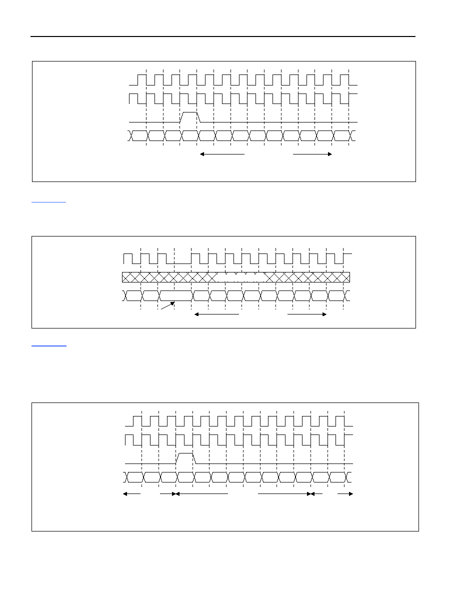
Figure 7-1
shows the polling and cell transfer cycles to UTOPIA ports in the DS26102. Note that UT_SOC must be
aligned with the first byte transfer. The DS26102 uses UT_SOC to detect the first byte of a cell. If a spurious
UT_SOC comes during a cell transfer, then the DS26102 aligns with the latest UT_SOC and ignores the bytes
(partial cell) received thus far.
7.1 UTOPIA-Side Transmit--Muxed Mode with 1 TXCLAV
In Level 1 UTOPIA there is only one PHY layer device. It uses UT_CLAV to convey transfer status to the ATM
layer. In Level 2 UTOPIA only one MPHY port at a time is selected for a cell transfer. However, another MPHY port
can be polled for its UT_CLAV status, while the selected MPHY port (device) transfers data. The ATM layer polls
the UT_CLAV status of an MPHY port by placing its address on UT_ADDR. The MPHY port (device) drives
UT_CLAV during each cycle, following one with its address on the UT_ADDR lines. The ATM layer selects an
MPHY port for transfer by placing the desired MPHY port address onto UT_ADDR, when UT_ENB is deasserted
during the current clock cycle and asserted during the next clock cycle. All MPHY devices only examine the value
on UT_ADDR for selection purposes when UT_ENB is deasserted. The MPHY port is selected starting from the
cycle after its address is on the UT_ADDR lines and UT_ENB is deasserted; a new MPHY port is addressed for
selection ending in the cycle and UT_ENB is deasserted. Once a MPHY port is selected, the cell transfer is
accomplished as described by the cell-level handshake of UTOPIA Level 1. To operate an MPHY device in a single
PHY environment, the address pins should be set to the value programmed by the management interface.
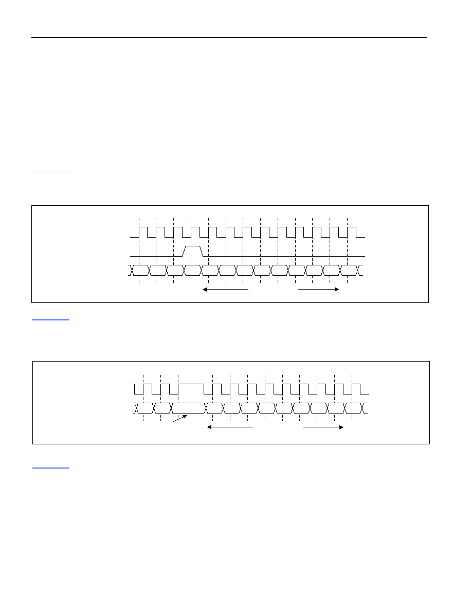
Figure 7-1
shows an example where PHYs are polled until the end of a cell transmission cycle. The UT_CLAV
signal shows that PHYs N - 3 and N + 3 can accept cells and that PHY N + 3 is selected. The PHY is selected with
the rising clock edge 16. Immediately after the beginning of cell transmission to PHY N + 3, the ATM layer starts
polling again. Up to 26 PHYs can be polled using the 2-clock polling cycles shown in
Figure 7-1
. This maximum
value can only be reached if all responses occur in minimum delays, e.g., as the figure shows, where the response
of the last PHY is obtained with clock edge 15, immediately followed by the UT_ENB pulse to the PHYs. If an ATM
implementation needs additional clock cycles to select the PHY, fewer than 26 PHY can be polled during one cell
cycle. Note that if the ATM decides to select PHY N again for the next cell transmission, it could leave the UT_ENB
line asserted and start transmitting the next cell with clock edge 15. This results in back-to-back cell transmission.
Note that the active PHY (PHY N) is polled in octet P48. According to the UTOPIA Level 1 specification, the PHY's
UT_CLAV signal at this time indicates the possibility of a subsequent cell transfer. Polling of PHY N before octet
P44 would be possible, but it does not indicate availability of the next cell.
DS26102 16-Port TDM-to-ATM PHY
18 of 64
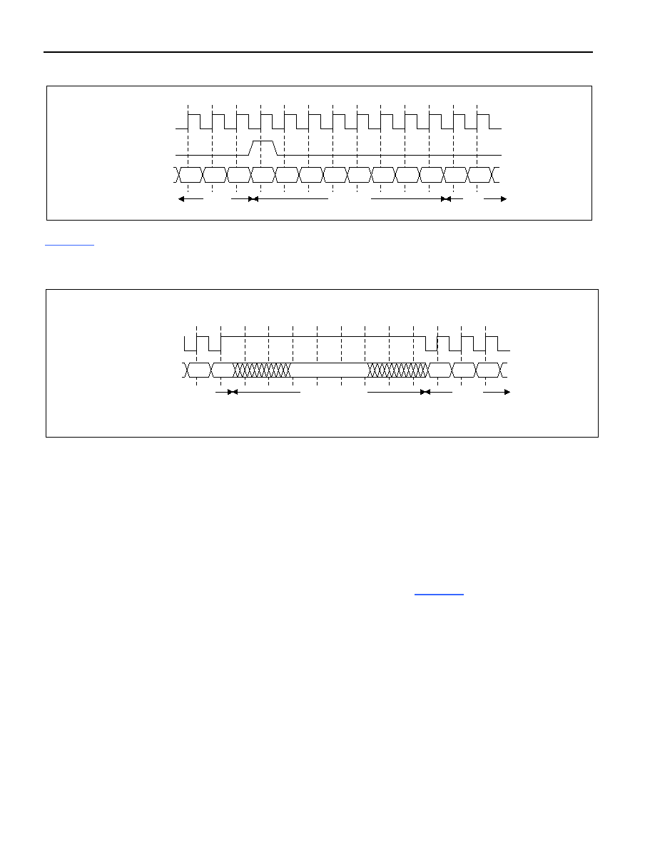
Figure 7-2
shows an example where the transmission of cells through the transmit interface is stopped by the ATM,
as no PHY is ready to accept cells. Polling then continues. Several clock cycles later one PHY gets ready to accept
a cell. During the transmission pause the UT_DATA and UT_SOC may go into high-impedance state, as shown in
Figure 7-2
. UT_ENB is held in deasserted state. When a PHY is found that is ready to accept a cell (PHY_N + 3 in
this case), the address of this PHY must be applied again to select it. This is necessary because of the 2-clock
polling cycle, where the PHY is detected at clock edge 15. At this time, the address of PHY N + 3 is no longer on
the bus, therefore, it must be applied again in the next clock cycle. PHY N + 3 is selected with clock edge 16.
Figure 7-1. Polling Phase and Selection Phase at Transmit Interface
Figure 7-2. End and Restart of Cell at Transmit Interface
N+1
1F
N-3
1F
N-2
1F
N-1
1F
N+3
N+1
1F
N
1F
N+3
1F
N+1
1F
N-1
1F
N+2
N-3
N-2
N-1
N+3
N+1
N
N+3
N+1
P35
P36
P37
P38
P39
P40
P41
P42
P43
P45
P46
P47
P48
H1
H2
H3
H4
P44
1
2
3
4
5
6
7
8
9
10
11
12
13
14
15
16
17
18
19
20
UT_CLK
UT_ADDR[4:0]
UT_CLAV[0]
UT_ENB
UT_DATA[7:0]
UT_SOC
CELL XMIT TO:
PHY N
PHY N+3
POLLING
POLLING
SELECTION
N+1
1F
N
1F
N+3
1F
N+2
1F
N-1
N
1F
N+3
1F
N+3
1F
N-2
1F
N-3
1F
N
P45
P46
P47
P48
H1
H2
H3
H4
1
2
3
4
5
6
7
8
9
10
11
12
13
14
15
16
17
18
19
20
UT_CLK
UT_ADDR[4:0]
UT_CLAV[0]
UT_ENB
UT_DATA[7:0]
UT_SOC
CELL XMIT TO:
PHY N
PHY N+3
POLLING
POLLING
SELECTION
N+1
N
N+3
N+2
N-1
N+3
N+3
N-2
DETECTION
DS26102 16-Port TDM-to-ATM PHY
19 of 64
Figure 7-3
shows an example where the ATM must pause the data transmission, as it has no data available (in this
case, for three clock cycles). This is done by deasserting UT_ENB and (optionally) setting UT_DATA and UT_SOC
into high-impedance state. Polling may continue. In the last clock cycle, before restarting the transmission, the
address "M" of the previously selected PHY is put on the UT_ADDR bus to reselect PHY M again.
Figure 7-3. Transmission to PHY Paused for Three Cycles
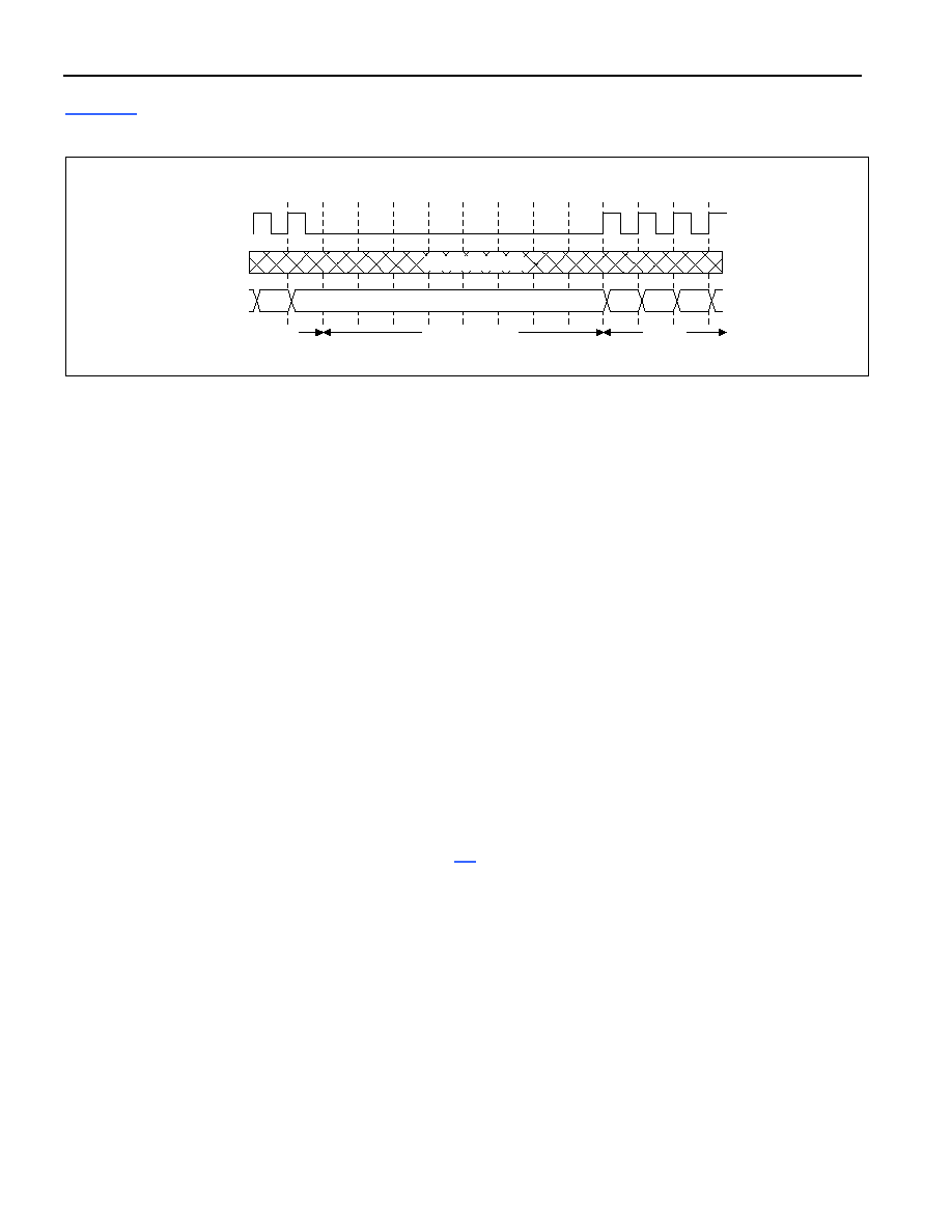
7.2 UTOPIA-Side Transmit--Direct Status Mode (MULTITXCLAV)
The DS26102 supports direct status mode per af-phy-0039.000 for a maximum of four PHY ports connected to one
ATM layer. For each PHY port, the status signals UR_CLAV and UT_CLAV are permanently available, according
to UTOPIA Level 1 specification. PHY devices with up to four on-chip PHY ports have up to four UR_CLAV and up
to four UT_CLAV status signals, one pair of UR_CLAV and UT_CLAV for each PHY port.
Status signals and cell transfers are independent of each other. No address information is needed to obtain status
information. Address information must be valid only for selecting a PHY port prior to one or multiple cell transfers.
With respect to the status signals UR_CLAV and UT_CLAV, this mode of operation corresponds to that of four
individual PHY devices, according to UTOPIA Level 1. With respect to the cell transfer, this mode of operation
corresponds to that as described in other parts of this document. The ATM layer selects a PHY port for cell transfer
by placing the desired port on the address lines (UR_ADDR[4:0], UT_ADDR[4:0]), while the enable signal
(
UR_ENB, UT_ENB) is deasserted. All PHY ports only examine the value on the address lines for possible selection
when the enable signal is deasserted. In case the ATM suspends transmission for a specific PHY port during a cell
transfer, no cells to/from other PHY ports can be transferred during this time.
Figure 7-4
shows a direct status example for the transmit direction. Signals UT_CLAV[3:0] are associated with PHY
port addresses 4, 3, 2, and 1. There is no need for a unique null device, therefore, "X = don't care" represents any
address between 0 and 31 on the address lines UT_ADDR[4:0] or any data on the data bus. In this mode, the
DS26102 supports address
ranges 0 to 3, 8 to 11, 16 to 19, or 24 to 27. In
Figure 7-4
the polling of PHY ports
starts while no cell transfer takes place. The ATM layer has pending cells for all four PHY ports (one individual
queue for each PHY port), but all four PHY ports cannot accept a cell. With rising clock edge 2, PHY port 1
indicates that it can accept a complete cell (UT_CLAV0 asserted). The ATM layer detects this at clock edge 3. It
selects that PHY port by placing address 1 on the address lines with rising clock edge 3. PHY port 1 detects this at
clock edge 4. At clock edge 5, PHY port 1 detects UT_ENB asserted, thus cell transfer for PHY port 1 starts with
rising clock edge 5 (byte H1).
N
1F
N+1
1F
N-4
1F
M
1F
N+2
N+3
1F
1F
N
N+1
N-4
M
N+2
N+3
P31
P32
P33 P34
P35 P36
P38 P39
P37
1
2
3
4
5
6
7
8
9
10
11
12
13
UT_CLK
UT_ADDR[4:0]
UT_CLAV[0]
UT_ENB
UT_DATA[7:0]
UT_SOC
CELL XMIT TO:
PHY M
POLLING
PHY M
PAUSE
XMIT
POLLING
SELECTION
DS26102 16-Port TDM-to-ATM PHY
20 of 64
At clock edge 5, the ATM layer detects a cell available at PHY port 3 (UT_CLAV2 asserted). With rising clock edge
52, PHY port 1 indicates that it cannot accept an additional cell by deasserting UT_CLAV0. Thus, at clock edge 57,
the ATM layer detects only UT_CLAV2 asserted (UT_CLAV1 and UT_CLAV3 remain deasserted). The ATM layer
deselects PHY port 1 and selects PHY port 3 for cell transfer with rising clock edge 57 by placing address 3 on the
address lines and deasserting UT_ENB. PHY port 1 and PHY port 3 detect this at clock edge 58. At clock edge 59,
PHY port 3 detects
UT_ENB asserted, thus cell transfer for PHY port 3 starts with rising clock edge 59 (byte H1).
For additional examples, refer to ATM Forum document af-phy-0039.000.
Figure 7-4. Example of Direct Status Indication, Transmit Direction
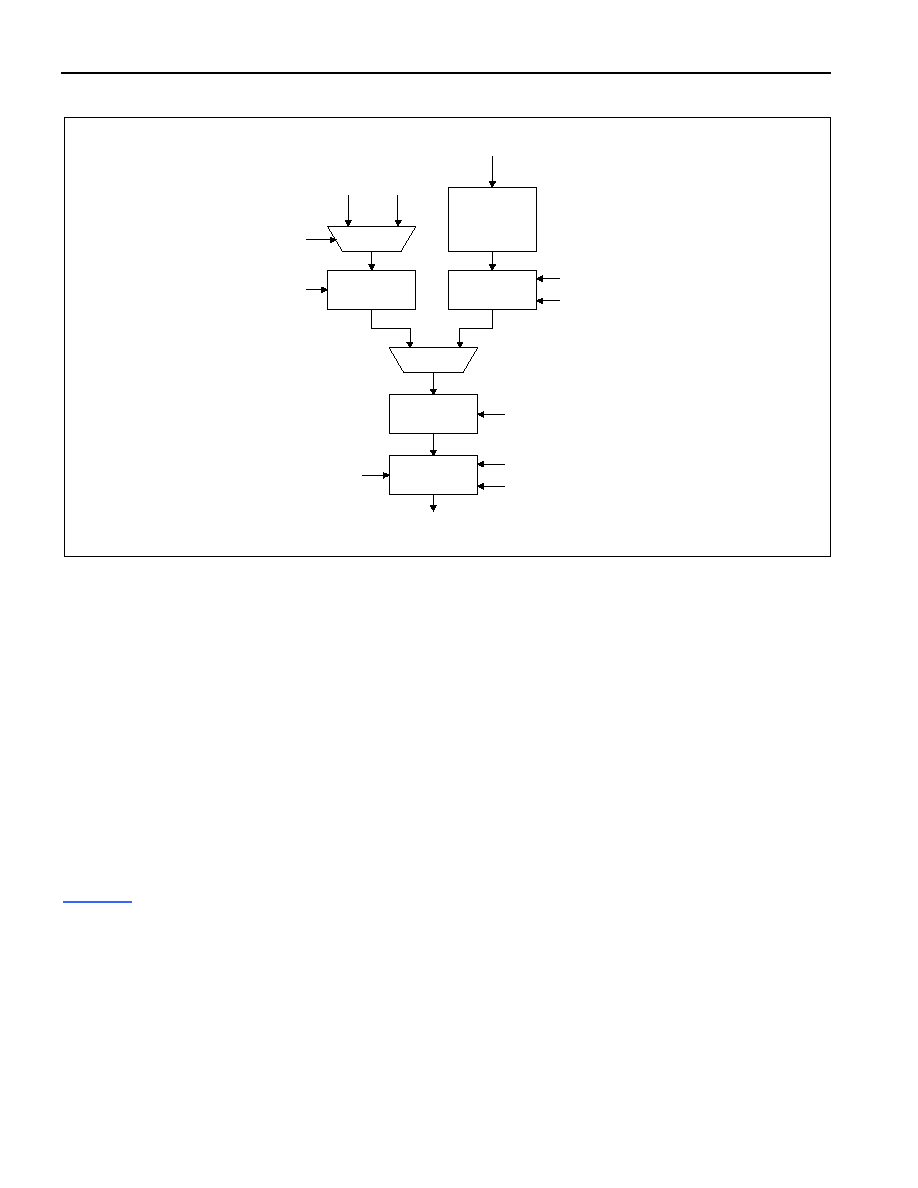
7.3 Transmit
Processing
The DS26102 can insert a valid HEC byte in the cell header, or it can be programmed to transparently transmit the
HEC byte from ATM layer. When inserting a valid HEC byte, COSET (0x55) addition can be disabled. The
generator polynomial used is 1 + X + X
2
+ X
8
. For idle/unassigned cell insertion (used for cell-rate decoupling), the
DS26102 inserts a valid HEC byte with or without COSET addition, depending on the TCRDS (TCR1.3)
microprocessor register bit. The DS26102 can scramble payload bytes, depending on the TPSE (TCR1.4) register
bit. The polynomial used for scrambling is X
43
+ 1. For debugging purposes, the DS26102 can be configured to
introduce a single-bit HEC error in the cell header of transmitted cells. When configured in HEC error-insertion
mode, the DS26102 inserts HEC errors in "HEC on period" number of cells and turns off HEC error insertion for
"HEC off period" number of cells, as set in the transmit HEC error-pattern register (THEPR). This process repeats
periodically until HEC error insertion is disabled through the THEIE bit (TCR1.1).
N-4
1
2
3
4
5
6
53
54
55
56
57
58
UT_CLK
UT_ADDR[4:0]
UT_CLAV0
UT_ENB
UT_SOC
59
H1
P45 P46
P48
X
P47
UT_DATA[7:0]
X
1
X
X = Don't Care
3
X
UT_CLAV1
UT_CLAV2
UT_CLAV3
PORT 1
PORT 2
PORT 3
PORT 4
H2
X
P44
H1
Port 1 Transfer
Port 3
52
DS26102 16-Port TDM-to-ATM PHY
21 of 64
Figure 7-5. Transmit Cell Flow and Processing
7.4 Physical-Side Transmit
The transmit framer interface operates in one of two modes:
1)
Gapped clock + data
2)
Clock + data + frame-pulse indication
The mode can be selected on a per-port basis by the TPLIM control bit (TCR2.1). If configured in frame-pulse-
indication mode, valid data bits are not sent during frame-pulse positions in the case of T1 and during TS0 and
TS16 positions in case of E1 direct mapping. The TS0 and TS16 locations are identified from the frame-pulse
indication signal aligned with bit 0 of the E1 frame. The TPC (TCFR.0) bit determines T1 or E1 configuration. ATM
cell octets are byte-aligned with respect to the frame-pulse-indication signal. In clear E1 mode, valid data bits are
transmitted at every clock tick. The DS26102 can either output the frame-pulse signal or use it as an input as
controlled through TFSD (TCR2.0).
The active edge of the transmit clock can be selected through the TAES control bit (TCR2.2). The active edge used
by the transmit interface should be configured to the opposite edge of that used by the external framer.
Figure 7-6
shows the transmit-framer-interface operation in frame-pulse mode for T1. In this example, the DS26102
uses the positive edge of TCLK to launch TDATA and TFP. Bit B1 is the MSB of a valid cell octet and B8 is the
LSB.
The TFP signal should be aligned with the framing bit position. When interfacing to framers where the framing
pulse and data active edges are individually configurable, it should be ensured that the sampling and updating
should happen in opposite edges.
UTOPIA II
Data Input
Transmit
FIFO
HEC Insertion
ON/OFF
HEC Insertion
ON
Payload
Scrambling
ON/OFF
HEC Error
Insertion
ON/OFF
Idle
Cell
Unassigned
Cell
TCRDS
(TCR1.3)
TCAE
(TCR1.2)
THIE (TCR1.0)
TCAE (TCR1.2)
TPSE (TCR1.4)
THEIE (TCR1.1)
HONP[4:0]
(THEPR)
HOFFP[2:0]
(THEPR)
Cell Data
to Framer (PHY)
DS26102 16-Port TDM-to-ATM PHY
22 of 64
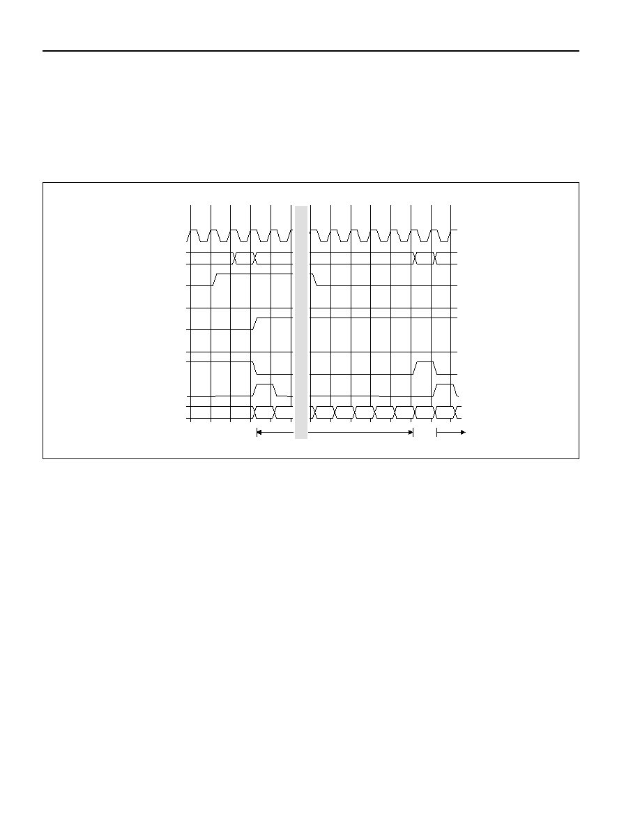
Figure 7-6. Transmit Framer Interface in TFP Mode for T1
Figure 7-7
shows the transmit-framer-interface operation for T1 in gapped-clock mode. The framing overhead-bit
position is gapped. In this diagram, DS26102 uses the positive edge to launch TDATA.
Figure 7-7. Transmit Framer Interface in Gapped-Clock Mode for T1
Figure 7-8
shows the E1 transmit-framer-interface operation using TFP to indicate the beginning of the E1 frame.
The DS26102 uses the positive edge to launch TDATA and TFP. Using TFP, the DS26102 identifies TS0 and
TS16 slots and does not send valid data on TDATA in these slots. In this case, B0 to B7 are not valid data bits of a
cell so that B8 is the MSB of the cell octet. The timing requirements for the TFP signal are the same as in the T1
case.
Figure 7-8. Transmit Framer Interface in TFP Mode for E1
TCLK[x]
1
TCLK[x]
2
TFP[x]
3
TDATA[x]
1) TCLK negative edge active
2) TCLK positive edge active
3) TFP as input or output
DSO Channel 1
F
B192
B191
B190
B1
B2
B3
B4
B5
B6
B7
B8
B9
TCLK[x]
TFP[x]
TDATA[x]
DSO Channel 1
TFP is Don't Care
F-Bit Gapped
B191
B190
B1
B2
B3
B4
B5
B6
B7
B8
B9
B192
TCLK[x]
1
TCLK[x]
2
TFP[x]
3
TDATA[x]
1) TCLK negative edge active
2) TCLK positive edge active
3) TFP as input or output (TFP_IN or TFP_OUT)
TS0 Slot
TS31
TS1
B0
B255
B254
B253
B1
B2
B3
B4
B5
B6
B7
B8
B9
DS26102 16-Port TDM-to-ATM PHY
23 of 64
Figure 7-9
shows the transmit framer-interface operation for E1 in gapped-clock mode.
Figure 7-9. Transmit Framer Interface in Gapped-Clock Mode for E1
The fractional T1 (N x DS0) is supported in TFP and gapped-clock modes of the physical interface. In TFP mode,
the framer must generate TFP during frame-overhead-bit and nonactive-DS0-channel positions. Fractional T1 is
not supported if TFP is generated by the DS26102. In gapped-clock mode, TCLK should be gapped during frame-
overhead-bit and nonactive-DS0-channel positions. In E1, to achieve a rate in multiples of 64kbps up to
2.048Mbps, the DS26102 should be configured in gapped-clock mode, and TCLK should be gapped during
nonactive time slots. TFP mode (for both input and output TFP configurations) is not supported in fractional E1
configuration.
The DS26102 can either use the T1/E1 clock from the framer or use an internally generated low-frequency clock at
the transmit line interface. The low-frequency clock is the system clock (1/2 x GCLKIN) divided by 8. This clock is
used primarily for diagnostic loopback.
The TLICS bit (TCR2.6) selects between the framer clock and the internally generated clock. The internally
generated clock should be used only in diagnostic loopback (otherwise, the framer and DS26102 are
operating for different clocks). During diagnostic loopback, this clock is fed to the receive line interface
unit.
8. RECEIVE OPERATION
The receive interface of the DS26102 is fully compliant to the ATM Forum's UTOPIA Level 2 specifications. Each
octal block of the DS26102 can be configured to use one of the address ranges (0 to 7, 8 to 15, 16 to 23, and 24 to
30) as UTOPIA port addresses. If Rx FIFO is not empty, cell available is asserted. After cell transfer from a port,
the external cell-available signal is updated based on the receive-FIFO fill level one clock cycle after cell transfer
completion. During this one-clock cycle, cell-available indication for this port is kept in the deasserted state. In other
words, one-clock minimum latency between two cell transfers from the same UTOPIA port is needed by the
DS26102 to update its internal cell pointers. Section
8.3
gives additional details concerning the UTOPIA-side
interface.
8.1 Physical-Side
Receive
The receive framer interface operates in one of two modes:
1)
Gapped clock + data
2)
Clock + data + frame-pulse indication
The mode can be selected on a per-port basis with the receive physical-layer interface mode control bit (RPLIM) at
RCR2.1. If configured in frame-pulse-indication mode, the bits coming at frame-pulse-indication positions are
ignored in case of T1 direct mapping, and bits coming at TS0 and TS16 positions are ignored in case of E1 direct
mapping. TS0 and TS16 slots are identified using the frame-pulse indication aligned with bit 0 of the E1 frame. The
control bit RPC (RCFR.0) determines T1 or E1 configuration. If no frame-pulse indication is given, bits are sampled
at every receive clock tick. If clear E1 operation is needed, the interface should be configured to operate in gapped
TCLK[x]
TFP[x]
TDATA[x]
TS31
TFP is Don't Care
TS0 (gapped)
TS1
B254
B8
B9
B10
B255
DS26102 16-Port TDM-to-ATM PHY
24 of 64
clock + data mode, in which case the external frame-pulse-indication signal is ignored and the data bits are clocked
at every clock tick.
The active edge of the receive clock can be selected through the RAES (RCR2.2) control bit. The active edge
selected for the Rx framer interface should be opposite the active edge that is used by the transmitting device
(either an external framer or the transmit section of DS26102, when enabled for diagnostic loopback).
Diagnostic loopback toward the ATM layer side (UTOPIA side) can be enabled through the DLBE (RCR2.0) control
bit. In diagnostic loopback, data, clock, and frame-pulse indication generated by the transmit section of the
DS26102 are used instead of the corresponding signals from the physical layer device. Rx physical-interface mode
should be configured with same value as the Tx physical-interface mode. The Rx active-edge selection bit should
be configured as the opposite edge of that used by the transmit section of the DS26102.
Figure 8-1
shows the receive framer-interface operation for T1 mode with the DS26102 using the positive clock
edge to sample RDATA and RFP and the framer using the negative edge to launch RDATA and RFP.
Figure 8-1. Receive Framer Interface in RFP Mode for T1
Figure 8-2
shows the receive-framer-interface operation for T1 in gapped-clock mode. The framing overhead-bit
position is gapped. In this figure, the DS26102 uses the positive edge to sample RDATA and RFP. RFP is don't
care.
Figure 8-2. Receive Framer Interface in Gapped-Clock Mode for T1
Figure 8-3
shows the receive-framer-interface operation for E1 using RFP to indicate the beginning of the E1
frame. The DS26102 uses the positive edge of RCLK to sample RDATA and RFP. Using RFP, the DS26102
identifies TS0 and TS16 slots and ignores RDATA coming in these slots.
RCLK[x]
RFP[x]
RDATA[x]
DSO Channel 1
F
B192
B191
B190
B1
B2
B3
B4
B5
B6
B7
B8
B9
RCLK[x]
RDATA[x]
DSO Channel 1
F-Bit Gapped
B192
B191
B190
B1
B2
B3
B4
B5
B6
B7
B8
B9
DS26102 16-Port TDM-to-ATM PHY
25 of 64
Figure 8-3. Receive Framer Interface in RFP Mode for E1
Figure 8-4
shows the receive-framer-interface operation for E1 in gapped-clock mode. In this mode, RCLK is
gapped during TS0 and TS16 locations.
Figure 8-4. Receive Framer Interface in Gapped-Clock Mode for E1
The fractional T1 (N x DS0) is supported in both RFP and gapped-clock modes of physical interface. In RFP mode,
the framer must generate RFP during frame-overhead-bit and nonactive-DS0-channel positions. In gapped-clock
mode, RCLK should be gapped during frame-overhead-bit and nonactive-DS0-channel positions. In E1 mode, the
DS26102 should be configured in gapped-clock mode and RCLK should be gapped during nonactive time slots.
RFP mode is not supported in fractional E1 configuration.
8.2 Receive
Processing
The received bits, after ignoring framing-overhead bits, are checked for possible HEC pattern. The polynomial used
for HEC check is G(X) = 1 + X + X
2
+ X
8
, per ITU I.432. Clearing the microprocessor interface register bit RCSE
(RCR1.0) can disable the COSET subtraction (0x55).
The cell boundaries in the incoming bit stream are identified based on HEC.
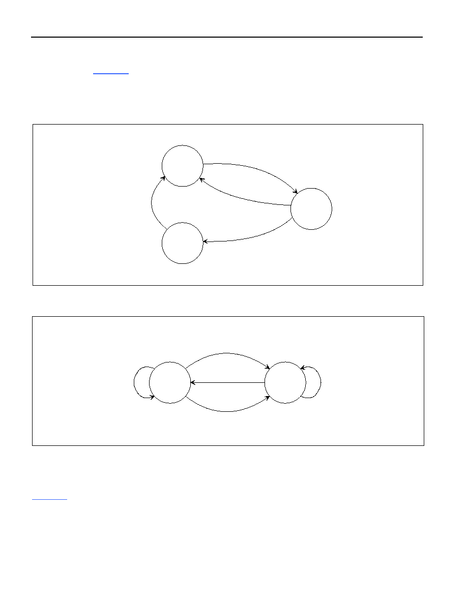
Figure 8-5
shows the cell-delineation
state machine. The cell-delineation state machine is initially in HUNT state. In HUNT state, it performs bit-by-bit
hunting for correct HEC. If correct HEC is found, it transitions to the PRESYNC state where it checks cell-by-cell for
correct HEC patterns. If DELTA-consecutive-correct patterns are received in PRESYNC, the cell-delineation state
machine transitions to SYNC state. Otherwise, it goes to HUNT state and reinitiates bit-by-bit hunting. In SYNC
state, if ALPHA-consecutive-incorrect HEC patterns are received, cell delineation is lost and it goes to HUNT state.
In PRESYNC and SYNC states, only cell-by-cell checking for the proper HEC pattern is performed. For the
DS26102, ALPHA = 7 and DELTA = 6.
The persistence of the out-of-cell delineation (OCD) event is integrated into LCD, based on programmable
integration time period (Rx-LCD integration-period register). If OCD persists for the programmed time, LCD is
declared. LCD is deasserted only when cell delineation persists in SYNC for the same-programmed integration
time. Whenever there is a change in LCD status (namely "into LCD" or "out of LCD"), an external interrupt is
generated when enabled by the corresponding mask bit RCR2.4. The persistence is checked every system clock
period (SYS_CLK) divided by 16,383. The default value of the Rx LCD integration-period register provides for an
integration time of 100ms for a 16.5MHz SYS_CLK.
RCLK[x]
RFP[x]
RDATA[x]
TS0 Slot
TS31
TS1
B0
B255
B254
B253
B1
B2
B3
B4
B5
B6
B7
B8
B9
RCLK[x]
RDATA[x]
TS31
TS0 (gapped)
TS1
B8
B9
B10
B255
B254
Don't Care
DS26102 16-Port TDM-to-ATM PHY
26 of 64
If single-bit header-error correction is enabled, the receiver mode of operation state machine follows the state
machine given in
Figure 8-6
. Single-bit correction is done only if correction is enabled and the state machine is in
the correction mode of operation at the start of cell transfer. Receiver mode of operation is valid only when cell
delineation is in SYNC state. The DS26102 maintains 8-bit correctable and 12-bit uncorrectable HEC-errored cell
counts. Both of these counters saturate.
Figure 8-5. Cell Delineation State Diagram
Figure 8-6. Header Correction State Machine
HEC error correction is performed based on receiver mode of operation. In correction mode, only single bit errors
can be corrected and the receiver switches to detection mode. In detection mode, all cells with detected header
errors are discarded, provided the receive-pass HEC-errored cells (RPHEC) control bit (RCR1.3) is clear. When a
header is examined and found not to be in error, the receiver switches to correction mode. The term "no action" in
Figure 8-6
means no correction is performed and no cell is discarded.
The payload bytes of the cell are descrambled using the self-synchronizing descrambler polynomial
X
43
+ 1, as given in ITU-T I.432. The descrambling can be enabled through the RDE control bit (RCR1.2).
Descrambling is activated if cell delineation is in PRESYNC or SYNC state. The cell header is not affected by
descrambling.
HUNT
PRESYNC
SYNC
Bit by Bit
Correct
HEC
Incorrect
HEC
Cell
by
Cell
DELTA
Consecutive
Correct HEC
ALPHA
Consecutive
Incorrect HEC
Cell by Cell
CORRECTION
MODE
DETECTION
MODE
Multibit Error
Detected
(Cell Discarded)
Single Bit Error
Detected
(Correction)
No Error Detected
(No Action)
No Error
Detected
(No Action)
Error Detected
(Cell Discarded)
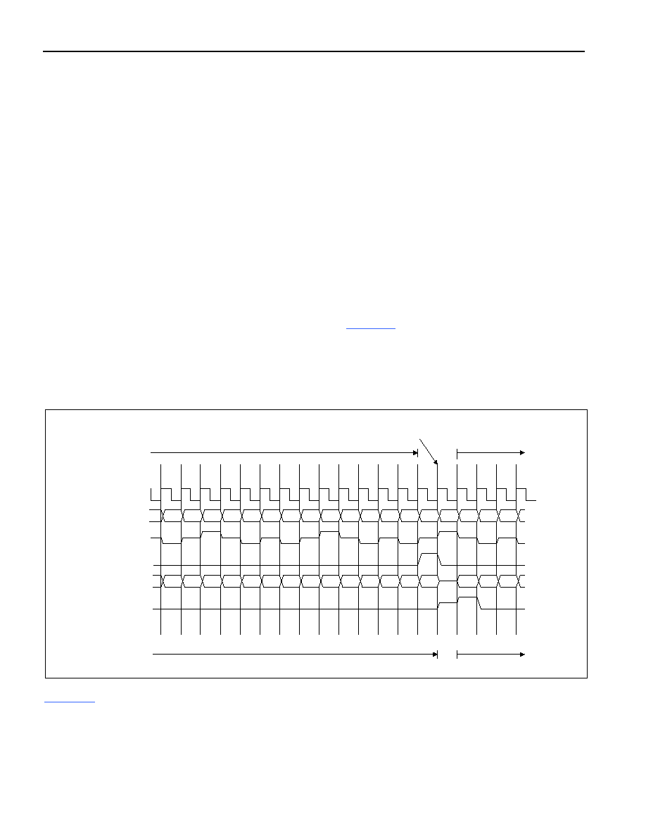
DS26102 16-Port TDM-to-ATM PHY
27 of 64
After descrambling and single-bit header-error correction, the cells are written into the receive FIFO as long as cell
delineation is in SYNC and the Rx FIFO is not full. Idle and/or unassigned cells can be filtered when enabled in the
receive control registers. Uncorrectable HEC-errored cells are normally
filtered and are not written into the Rx FIFO
unless RPHEC (RCR1.3) is set. Note that if HEC error correction is disabled, all HEC-errored cells are termed as
uncorrectable HEC-errored cells. A 16-bit counter tracks the number of cells that can be written into the Rx FIFO
and saturates at 0xFFFF. Note that, whether or not the ATM layer dequeues cells from Rx FIFO, this counter is
incremented if valid cells are received. This counter is cleared by the microprocessor interface once it is latched. A
4-cell buffer per port is maintained for rate decoupling.
8.3 UTOPIA-Side Receive--Muxed Mode with 1 RXCLAV
An internal version of the cell-available signal is maintained per port. The DS26102 drives the internal cell-available
signals onto the external CLAV lines based on the configured polling mode. In direct status mode, only four ports
are supported. The four external CLAV lines are driven with the corresponding internal CLAV signals for UTOPIA
ports 0 to 3. In multiplexed-with-1-CLAV mode, only CLAV [0] is driven with the cell-available signal for the port
corresponding to the current lower three UTOPIA address bits. The upper two UTOPIA address bits should match
the configured address range. If cell transfer is going on for a port, its CLAV is kept asserted until the last byte is
transferred to the ATM layer. This is accomplished to support interfacing with the octet-level ATM layer as well. The
ATM layer must poll cell-available status for any fresh cell corresponding to a port only after the current cell transfer
to the port is completed.
The multiplexed with 1 CLAV polling-mode cycle is depicted in
Figure 8-7
, in which N, N + 2, N - 3, N - 2, N - 1,
N + 3, N + 1 are considered part of the DS26102 UTOPIA ports. During reception of a cell from PHY N, the other
PHYs are polled. It turns out that PHY N - 3 and PHY N + 3 have cells available, and PHY N + 3 is ultimately
selected. Just like the transmit interface, the 2-clock polling cycle allows a maximum of 26 PHYs to be polled in the
8-bit mode during a cell transfer.
Figure 8-7. Polling Phase and Selection at Receive Interface
Figure 8-8
shows a case when, after the end of transmission of a cell from PHY N, no other PHY has a cell
available. Therefore,
UR_ENB remains asserted as the ATM assumes a cell available from PHY N. With clock
edge 9, PHY N also has no cell available, as UR_SOC remains low. The ATM then deasserts
UR_ENB while the
polling of the PHYs continues. With clock edge 15, PHY N - 3 is found to have a cell for transmission. So address
N - 3 is applied, and the PHY N - 3 is selected with clock edge 16. Additional receive interface examples are
available in ATM Forum's af-phy-0039.000.
N+2
1F
N-3
1F
N-2
1F
N-1
1F
N+3
N+1
1F
N-1
1F
N+3
1F
N+1
1F
N-1
1F
N+2
N-3
N-2
N-1
N+3
N+1
N+3
N+1
P35
P36
P37
P38
P39
P40 P41 P42 P43
P45 P46 P47 P48
H1
H2
H3
P44
1
2
3
4
5
6
7
8
9
10
11
12
13
14
15
16
17
18
19
UR_CLK
UR_ADDR[4:0]
UR_CLAV[0]
UR_ENB
UR_DATA[7:0]
UR_SOC
CELL RCV FROM:
PHY N
PHY N+3
POLLING
POLLING
SELECTION
N-1
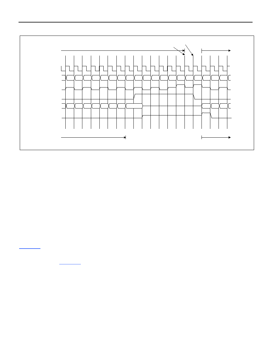
DS26102 16-Port TDM-to-ATM PHY
28 of 64
Figure 8-8. End and Restart of Cell Transmission at Receive Interface
8.4 UTOPIA-Side Receive--Direct Status Mode (MULTIRXCLAV)
Consider up to a maximum of four PHY ports connected to one ATM layer. For each PHY port, the status signals
UR_CLAV and UT_CLAV are permanently available according to UTOPIA Level 1 specification. PHY devices with
up to four on-chip PHY ports have up to four UR_CLAV and up to four UT_CLAV status signals, one pair of
UR_CLAV and UT_CLAV for each PHY port.
Status signals and cell transfers are independent of each other. No address information is needed to obtain status
information. Address information must be valid only for selecting a PHY port prior to one or multiple cell transfers.
With respect to the status signals UR_CLAV and UT_CLAV, this mode of operation corresponds to that of four
individual PHY devices, according to UTOPIA Level 1. With respect to the cell transfer, this mode of operation
corresponds to that described in this document and af-phy-0039.000. The ATM layer selects a PHY port for cell
transfer by placing the desired port on the address lines (UR_ADDR[4:0], UT_ADDR[4:0]), while the enable signal
(UR_ENB, UT_ENB) is deasserted. All PHY ports only examine the value on the address lines for possible selection
when the enable signal is deasserted. If the ATM layer suspends transmission for a specific PHY port during a cell
transfer, no cells to/from other PHY ports can be transferred during this time.
Figure 8-9
shows an example for the receive direction. The status signals UR_CLAV[3:0] are associated with PHY
port addresses 4, 3, 2, and 1. Note that for the DS26102, the address range can be any one of 0 to 3, 8 to 11, 16 to
19, and 24 to 27. There is no need for a unique null device, so "X = don't care" on the address lines
UR_ADDR[4:0]. In
Figure 8-9
the polling of PHY ports starts while no cell transfer takes place. The ATM layer
monitors all four status signals UR_CLAV[3:0]. At clock edge 3, it detects a cell available at PHY port 1
(UR_CLAV0 asserted). It selects that PHY port by placing address 1 on the address lines with rising clock edge 3.
PHY port 1 detects this at clock edge 4. At clock edge 5, PHY port 1 detects
UR_ENB asserted, thus cell transfer
for PHY port 1 starts with rising clock edge 5.
At clock edge 5, the ATM layer detects a cell available at PHY port 3 (UR_CLAV2 asserted). Not knowing whether
PHY port 1 may have another cell available or not, the ATM layer deselects PHY port 1 and selects PHY port 3 for
cell transfer with rising clock edge 57 by placing address 3 on the address lines and deasserting UR_ENB. PHY
port 1 and PHY port 3 detect this at clock edge 58. At clock edge 59, PHY port 3 detects UR_ENB asserted, thus
cell transfer starts with rising clock edge 59. At clock edge 111, no cell is available at PHY ports 1, 2, and 4. The
ATM layer keeps
UR_ENB asserted and detects at clock edge 113 the first byte of another cell available from PHY
port 3 (UR_CLAV2 asserted). Thus, cell transfer takes place starting with rising clock edge 112. At clock edge 164,
again, no cell is available at PHY ports 1, 2, and 4. The ATM layer keeps the
UR_ENB asserted and detects at
N-3
1F
N+1
1F
N-1
1F
N
1F
N+3
N-1
1F
N-3
1F
N-3
1F
N+1
1F
N+2
1F
N-1
H1
H2
H3
1
2
3
4
5
6
7
8
9
10
11
12
13
14
15
16
17
18
19
20
UR_CLK
UR_ADDR[4:0]
UR_CLAV[0]
UR_ENB
UR_DATA[7:0]
UR_SOC
CELL RCV FROM:
PHY N
PHY N-3
POLLING
POLLING
SELECTION
N-3
N+1
N-1
N
N+3
N-3
N-3
N+1
DETECTION
P45
P46
P47 P48
P42
P43
P44
XX
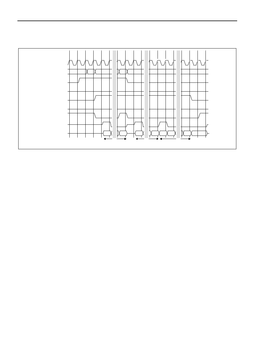
DS26102 16-Port TDM-to-ATM PHY
29 of 64
clock edge 166 that there also is no cell available from PHY port 3 (UR_CLAV2 deasserted). Thus, the ATM layer
deselects PHY port 3 by deasserting
UR_ENB with rising clock edge 166.
Figure 8-9. Example Direct Status Indication, Receive Direction
1
2
3
4
5
6
58
59
60
112
113
UR_CLK
UR_ADDR[4:0]
UR_CLAV0
UR_ENB
UR_SOC
114
H1
H1
P48
H1
UR_DATA[7:0]
X
1
X
UR_CLAV1
UR_CLAV2
UR_CLAV3
PORT 1
PORT 2
PORT 3
PORT 4
P48
H2
57
165
166
167
111
164
3
X
X
X
TRI-STATED
P48
X
CELL TRANSFER
(PORT 1)
CELL TRANSFER
(PORT 3)
CELL TRANSFER
(PORT 3)
DS26102 16-Port TDM-to-ATM PHY
30 of 64
9. REGISTER MAPPING
The 8-bit registers described in this section are maintained per port, unless otherwise noted. Address bits [7:5]
determine port number, address bit [4] distinguishes Tx and Rx section registers, and address bits [3:0] select the
particular register in Tx and Rx sections. This register arrangement applies to each block of eight T1/E1 ports. The
DS26102 contains two octal blocks that are selected with the BLS signal.
Table 9-A. Register Map
P1 P2 P3 P4 P5 P6 P7 P8 R/W
REGISTER FUNCTION
00 -- -- -- -- -- -- -- RW
TCFR
Tx Configuration Register (Note 1)
-- 20 40 60 80 A0 C0 E0 --
--
Reserved (Note 2)
01 21 41 61 81 A1 C1 E1 W
TPCL
Tx PMON Counter Latch-Enable Register
02 22 42 62 82 A2 C2 E2 R
TACC1
Tx-Assigned Cell Counter MSB (Note 3)
03 23 43 63 83 A3 C3 E3 R
TACC2
Tx-Assigned Cell Counter LSB (Note 4)
04 -- -- -- -- -- -- -- RW
TIUPB
Tx Idle/Unassigned Payload Byte (Note 1)
-- 24 44 64 84 A4 C4 E4 --
--
Reserved (Note 2)
05 -- -- -- -- -- -- -- RW
THEPR
Tx HEC Error-Insertion Pattern (Note 1)
-- 25 45 65 85 A5 C5 E5 --
--
Reserved (Note 2)
06 26 46 66 86 A6 C6 E6 RW
TCR1
Tx Control Register 1
07 27 47 67 87 A7 C7 E7 RW
TCR2
Tx Control Register 2
08 -- -- -- -- -- -- -- R
ISR
Interrupt Status Register (Note 1)
09
to
0F
28
to
2F
48
to
4F
68
to
6F
88
to
8F
A8
to
AF
C8
to
CF
E8
to
EF
--
--
Reserved (Note 2)
10 -- -- -- -- -- -- -- RW
RCFR
Rx Configuration Register (Note 1)
-- 30 50 70 90 B0 D0 F0
Reserved
11 -- -- -- -- -- -- -- RW
RLCDIP
Rx LCD Integration Register (Note 1)
-- 31 51 71 91 B1 D1 F1 --
--
Reserved
12 32 52 72 92 B2 D2 F2 W
RPCL
Rx PMON Counter-Latch Enable
13 33 53 73 93 B3 D3 F3 R
RCHEC
Rx Correctable HEC Latch
14 34 54 74 94 B4 D4 F4 R
RUHEC1
Rx Uncorrectable HEC MSB
15 35 55 75 95 B5 D5 F5 R
RUHEC2
Rx Uncorrectable HEC LSB
16 36 56 76 96 B6 D6 F6 R
RACC1
Rx-Assigned Cell Counter MSB (Note 5)
17 37 57 77 97 B7 D7 F7 R
RACC2
Rx-Assigned Cell Counter LSB (Note 6)
18 38 58 78 98 B8 D8 F8 R
PSR
Per Port Status Register
19 39 59 79 99 B9 D9 F9 RW
RCR1
Rx Control Register 1
1A 3A 5A 7A 9A BA DA FA RW
RCR2
Rx Control Register 2
1B 3B 5B 7B 9B BB DB FB RW
RUFC
Rx User-Filter Control
1C 3C 5C 7C 9C BC DC FC RW
RUFPM1
Rx User-Filter Pattern/Mask 1
1D 3D 5D 7D 9D BD DD FD RW
RUFPM2
Rx User-Filter Pattern/Mask 2
1E 3E 5E 7E 9E BE DE FE RW
RUFPM3
Rx User-Filter Pattern/Mask 3
1F 3F 5F 7F 9F BF DF FF RW
RUFPM4
Rx User-Filter Pattern/Mask 4
P1 to P8 = Address locations (hex) for UTOPIA PHY port 1 through port 8.
Note 1: These registers are common to all ports.
Note 2: Writing into reserved address regions should be avoided. Reading from reserved address regions could give undefined value.
Note 3: Tx-assigned cell counter MSB-latch register is an 8-bit register common to all ports. It can be accessed with any of the 8 addresses.
This register holds the upper 8-bit of the Tx-assigned-cell count for the port selected by accessing the Tx-PMON counter latch-enable
register.
Note 4: Tx-assigned cell counter LSB-latch register is an 8-bit register common to all ports. It can be accessed with any of the 8 addresses.
This register holds the lower 8-bit of the Tx-assigned cell count for the port selected by accessing the Tx-PMON counter latch-enable
register.
Note 5: Rx-assigned cell counter MSB-latch register is an 8-bit register common to all ports. It can be accessed with any of the 8 addresses.
This register holds the upper 8-bit of the Rx-assigned cell count for the port selected by accessing the Rx-PMON counter latch-enable
register.
Note 6: Rx-assigned cell counter LSB-latch register is an 8-bit register common to all ports. It can be accessed with any of the 8 addresses.
This register holds the lower 8-bit of the Rx-assigned cell count for the port selected by accessing the Rx-PMON counter latch-enable
register.
Conventions:
1) In bit definitions, bit 7 is the most significant bit (MSB) and bit 0 is the least significant bit (LSB).
2) Ports can be referred with either 1 to 8 (one-based) or 0 to 7 (zero-based). While referring a port, the addressing system, either one-based
or zero-based is explicitly mentioned in brackets.
DS26102 16-Port TDM-to-ATM PHY
31 of 64
3) Reserved bit fields should be replaced with 0 while writing and, upon reading, the value corresponding to reserved bit fields is undefined.
4) R indicates read permission; W indicates write permission; RW indicates read/write permission for software to access a register.
10. REGISTER
DEFINITIONS
10.1 Transmit
Registers
Register Name:
TCFR
Register Description:
Transmit Configuration Register
Register Address:
00h (Common for All Transmit Ports)
Bit:
7 6 5 4 3 2 1 0
Name: -- -- -- --
TADDR1
TADDR0
TPM
TPC
Default:
0 0 0 1 0 0 0 0
Bit 0: Transmit Port Configuration (TPC). This bit affects only the Tx section.
0 = T1 mode
1 = E1 mode
Bit 1: Transmit Poll Mode (TPM). Transmit UTOPIA polling mode configuration.
0 = multiplexed with 1CLAV mode
1 = direct status
Bits 2, 3: Transmit High Address (TADDR). These bits decide which upper 2 bits of the UTOPIA address are to
be used by the ATM layer for selecting one of the ports. The lower 3 bits of address are assigned to the port
number 1 to 8 (one-based):
'00' for address range 07
'01' for address range 815
'10' for address range 1623
'11' for address range 2430
*
Note that the address range selected when the BSL0 pin = 0 must be different than the address range selected
when BSL0 = 1.
Bits 3 to 7: Unassigned, read only
*Address 31 (1F hex) is reserved as the null address per UTOPIA forum. When an octal block is offset to the highest UTOPIA address range,
the port at address 31 becomes inactive.

DS26102 16-Port TDM-to-ATM PHY
32 of 64
Register Name:
TCR1
Register Description:
Transmit Control Register 1
Register Address:
06h, 26h, 46h, 66h, 86h, A6h, C6, E6h
Bit:
7 6 5 4 3 2 1 0
Name: -- TPEDIM
TPRS
TPSE
TCRDS
TCAE
THEIE
THIE
Default:
0 0 0 0 0 1 0 1
Bit 0: Transmit HEC Insertion Enable (THIE)
0 = HEC byte as received from the ATM layer is transparently passed.
1 = proper HEC value is computed and inserted into the HEC byte of the cell.
Bit 1: Transmit HEC Error-Insertion Enable (THEIE)
0 = HEC error insertion disabled
1 = HEC errors are introduced into the transmitted cells, as specified by the transmit HEC error-insertion
pattern register.
Bit 2: Transmit COSET Addition Enable (TCAE)
0 = no COSET addition
1 = COSET (0x55) addition to the calculated HEC. Note that if HEC insertion is disabled, the HEC byte is
transmitted transparently (this bit does not affect ATM layer cells). However, the HEC byte of
idle/unassigned cells used for cell-rate decoupling includes COSET addition as long as the TCAE bit is
enabled.
Bit 3: Transmit Cell-Rate Decoupling Selection (TCRDS)
0 = idle cell
1 = unassigned cell
Bit 4: Transmit Payload Scrambling Enable (TPSE)
0 = disable scrambling
1 = enable scrambling
Bit 5: Transmit Parity Select (TPRS). This bit determines the parity mode expected on the UT_PAR signal.
0 = odd parity check selected for transmit UTOPIA bus
1 = even parity check selected for transmit UTOPIA bus
Bit 6: Transmit Parity Error-Detect Interrupt Mask (TPEDIM)
0 = DS26102 does NOT generate an external interrupt on a Tx parity error.
1 = DS26102 does generate an external interrupt on a Tx parity error.
Bit 7: Unassigned, must be set to 0 for proper operation
DS26102 16-Port TDM-to-ATM PHY
33 of 64
Register Name:
TCR2
Register Description:
Transmit Control Register 2
Register Address:
07h, 27h, 47h, 67h, 87h, A7h, C7h, E7h
Bit:
7 6 5 4 3 2 1 0
Name: -- TLICS
FDC1
FDC0
TCES
TAES
TPLIM
TFSD
Default:
0 0 0 0 0 0 0 0
Bit 0: Transmit Frame-Sync Direction (TFSD)
0 = UTOPIA block accepts a transmit frame sync (TFP is an input).
1 = UTOPIA block generates a frame sync (TFP is an output).
Bit 1: Transmit Physical-Layer Interface Mode (TPLIM)
0 = clock + data + frame-pulse-indication combination
1 = gapped clock + data combination
Bit 2: Transmit Active-Edge Selection (TAES)
0 = positive edge of TCLK as timing reference
1 = negative edge of TCLK as timing reference
Bit 3: Transmit Clear E1 Selection (TCES)
0 = channelized E1 (data at TS0 and TS16 is ignored)
1 = clear E1 (all E1 channels are used)
Bits 4, 5: Transmit FIFO Depth Configuration Bits (FDC1, FDC0)
FDC1 FDC0
Cell
Depth
0 0
4
0 1
3
1 0
2
1 1 Reserved
Bit 6: Transmit Line Interface Clock Selection (TLICS)
0 = The T1/E1 clock from the framer (TCLKx) is used at the transmit line interface.
1 = The internally generated system clock divided by 8 is used at the transmit line interface.
Bit 7: Unassigned, must be set to 0 for proper operation
Register Name:
TPCL
Register Description:
Transmit PMON Counter Latch
Register Address:
01h, 21h, 41h, 61h, 81h, A1h, C1h, E1h
Bit:
7 6 5 4 3 2 1 0
Name: -- -- -- -- -- -- -- --
Default:
0 0 0 0 0 0 0 0
Bits 0 to 7: The host should always write 0x00 to this register when latching the PMON counter. This
register is provided for latching in the 16-bit transmit-assigned cell-count value of a port into the common transmit-
assigned cell-counter latch register. In order to read the transmit-assigned cell-count value, software writes into this
register and then reads from the Tx-assigned cell counter MSB and LSB registers. A write into this register clears
the value.
Figure 10-1
depicts the sequence of operation for accessing the Tx-assigned cell counter (TACC) for a
given port.
DS26102 16-Port TDM-to-ATM PHY
34 of 64
Figure 10-1. Accessing Tx PMON Counter
Register Name:
TACC1
Register Description:
Transmit-Assigned Cell-Count Register 1
Register Address:
02h, 22h, 42h, 62h, 82h, A2h, C2h, E2h (Common to All Ports)
Bit:
7 6 5 4 3 2 1 0
Name: TACC15 TACC14 TACC13 TACC12 TACC11 TACC10 TACC9 TACC8
Default:
0 0 0 0 0 0 0 0
Bits 0 to 7: Transmit-Assigned Cell Count (TACC8 to TACC15). This register is read-only.
Register Name:
TACC2
Register Description:
Transmit-Assigned Cell-Count Register 2
Register Address:
03h, 23h, 43h, 63h, 83h, A3h, C3h, E3h (Common to All Ports)
Bit
7 6 5 4 3 2 1 0
Name TACC7 TACC6 TACC5 TACC4 TACC3 TACC2 TACC1 TACC0
Default
0 0 0 0 0 0 0 0
Bits 0 to 7: Transmit-Assigned Cell Count (TACC0 to TACC7). This register is read-only. These registers are
common for all ports. For software convenience, any of the eight addresses can be used to access these registers.
The transmit-assigned cell-count value reflects the number of ATM layer cells transmitted since last latching. For
reading the 16-bit transmit-assigned cell count for a port, software must write into the transmit-PMON counter latch-
enable register for the desired port prior to reading these registers. Reading from these registers without writing
into the latch-enable register returns the old value that was latched and not the current value.
WHAT THE HOST MUST DO
HOW THE DS26101/DS26102 RESPONDS
DS26101/DS26102 LATCHES TX-ASSIGNED
CELL-COUNTER VALUE OF THE PORT
SELECTED INTO CORRESPONDING LATCH
REGISTER AND CLEARS THE INTERNAL
ASSIGNED CELL COUNTER OF THE PORT
FOR FRESH ACCUMULATION.
DS26101/DS26102 DRIVES MOST SIGNIFICANT
8 BITS (TACC[15:8]) OF LATCHED ASSIGNED
CELL-COUNT VALUE ONTO THE DATA BUS.
DS26101/DS26102 DRIVES LEAST SIGNIFICANT
8 BITS (TACC[7:0]) OF LATCHED ASSIGNED
CELL-COUNT VALUE ONTO THE DATA BUS.
WRITE 00 INTO Tx-PMON COUNTER LATCH
REGISTER (TPCL) FOR THE PORT WHOSE
COUNTER VALUE IS TO BE OBTAINED. NOTE
THAT ONLY THE ADDRESS SPECIFIC TO
THE PORT INTENDED MUST BE USED.
READ FROM Tx-ASSIGNED CELL COUNTER
LATCH REGISTER 1 (TACC1). NOTE THAT
ANY ONE OF THE EIGHT ADDRESSES
SPECIFIED FOR THIS REGISTER CAN BE
USED.
READ FROM Tx-ASSIGNED CELL COUNTER
LATCH REGISTER 2 (TACC2). NOTE THAT
ANY ONE OF THE EIGHT ADDRESSES
SPECIFIED FOR THIS REGISTER CAN BE
USED.
DS26102 16-Port TDM-to-ATM PHY
35 of 64
Register Name:
TIUPB
Register Description:
Transmit Idle/Unassigned Payload Byte Register
Register Address:
04h (Common for All Transmit Ports)
Bit:
7 6 5 4 3 2
1
0
Name: TIUP7 TIUP6 TIUP5 TIUP4 TIUP3 TIUP2 TIUP1 TIUP0
Default:
0 1 1 0 1 0
1
0
Bits 0 to 7: Transmit Idle/Unassigned Payload (TIUP0 to TIUP7). This register holds the payload byte to be
carried in octets of idle/unassigned cells, transmitted toward the line for cell-rate decoupling. This register defaults
to the value 6Ah.
Register Name:
THEPR
Register Description:
Transmit HEC Error-Insertion Pattern Register
Register Address:
05h (Common for All Transmit Ports)
Bit:
7 6 5 4 3 2
1
0
Name: HOFFP4 HOFFP3 HOFFP2 HOFFP1 HOFFP0 HONP2 HONP1 HONP0
Default:
0 0 1 0 1 0
0
1
Bits 0 to 2: HEC On Period (HONP0 to HONP2). This register holds the number of cells in which incorrect HEC
(HEC error insertion is ON) is sent, if HEC error insertion is enabled.
Bits 3 to 7: HEC Off Period (HOFFP0 to HOFFP4). This register holds the number of cells in which correct HEC
(HEC error insertion is OFF) is sent, if HEC error insertion is enabled.
If HEC error insertion in the transmit control register is enabled for a port (THEIE = 1), then for the "HEC off period"
cells are transmitted to the port with correct HEC; for the "HEC on period" cells are sent with incorrect HEC. This
cycle repeats until HEC error insertion is disabled. Note that HEC errors are inserted according to the above
pattern as long as THEIE is set, whether HEC insertion (THIE) is enabled or not.
10.2 Status
Registers
Register Name:
PSR
Register Description:
Port Status Register
Register Address:
18h, 38h, 58h, 78h, 98h, B8h, D8h, F8h
Bit:
7 6 5 4 3 2 1 0
Name: EXSTAT TPED CDS1 CDS0 RMS LCDS LCDCSIS FOIS
Default:
0 0 0 0 0 1 0 0
Bit 0: Receive FIFO-Overrun Interrupt Status (FOIS). This status bit is set when the receive FIFO overruns. It
creates an interrupt on the
INT pin if the Rx FIFO-overrun interrupt mask bit (RCR2.3) is set. This bit is reset when
read.
Bit 1: LCD Change-of-State Interrupt Status (LCDCSIS). This status bit is set when LCD status changes. It
creates an interrupt on the INT pin if the LCD interrupt mask bit (RCR2.4) is set. This bit is reset when read.
Bit 2: LCD Status (LCDS). The LCDS bit indicates the current status of LCD.
0 = in-cell delineation
1 = loss-of-cell delineation
Bit 3: Receiver Mode Status (RMS). This bit shows valid status only when HEC correction is enabled.
0 = correction mode
1 = detection mode
DS26102 16-Port TDM-to-ATM PHY
36 of 64
Bits 4, 5: Cell Delineation Status 0, 1 (CDS0, CDS1). These bits show the cell delineation status. Bit 5 indicates
instantaneous OCD status.
CDS1
CDS0
Cell Delineation Status
0 0
HUNT
State
0 1 PRESYNC
State
1 x
SYNC
State
Bit 6: Transmit Parity Error Detect (TPED). This bit is set for each transmit parity error that is detected on the
transmit UTOPIA interface. It can generate an interrupt when enabled by TPEDIM in TCR1. This bit is reset if read
access to this register is detected.
Bit 7: External Status Event (EXSTAT). This bit is set on the rising edge of the signal applied to the associated
EXSTAT signal. It can generate an interrupt when enabled by EXSTATIM in RCR2. This bit is reset if read access
to this register is detected. EXSTAT1 maps to this bit in the PSR for port 1 (18h) up to EXSTAT8, which maps to
the PSR for port 8 (F8h).
A typical application might connect the 1SECOUT signal created by the DS26102 to one of the EXSTAT signals so
that an interrupt can be created on 1-second boundaries. The EXSTAT signals, however, can also be used to
provide microprocessor access to board-level hardware-status pins or an off-chip interval timer.
Register Name:
ISR
Register Description:
Interrupt Status Register
Register Address:
08h (Common for All Ports)
Bit:
7 6 5 4 3 2 1 0
Name: PSR8 PSR7 PSR6 PSR5 PSR4 PSR3 PSR2 PSR1
Default:
0 0 0 0 0 0 0 0
The ISR register reports which of the 8 ports are currently generating interrupts. ISR.0 reports the status for port 1
(18h), while ISR.7 reports the status for port 8 (F8h). When the associated port's status register is read (and
consequently cleared), the associated bit in this register is also cleared. Note that only status bits that are enabled
to generate an interrupt (i.e., the interrupt mask bit is set) set the reporting bit in this register.
10.3 Receive Registers
Register Name:
RCFR
Register Description:
Receive Configuration Register
Register Address:
10h (Common for All Receive Ports)
Bit:
7 6 5 4 3 2 1 0
Name:
-- -- -- --
RADDR1
RADDR0
RUPM
RPC
Default:
0 0 0 1 0 0 0 0
Bit 0: Receive Port Configuration (RPC). This bit affects only the Rx section.
0 = T1 mode
1 = E1 mode
Bit 1: Receive Polling Mode (RUPM)
0 = multiplexed with 1CLAV mode
1 = direct status
Bits 2, 3: Receive High Address (RADDR). These bits decide which upper 2 bits of the UTOPIA address are to
be used by the ATM layer for selecting one of the ports. The lower 3 bits of address are assigned to port number 1
to 8 (one-based):
'00' for address range 07
'01' for address range 815
DS26102 16-Port TDM-to-ATM PHY
37 of 64
'10' for address range 1623
'11' for address range 2430
*
Note that the address range selected when the BSL0 pin = 0 must be different than the address range selected
when BSL0 = 1.
Bits 4 to 7: Unassigned, read only
*Address 31 (1F hex) is reserved as the null address per UTOPIA forum. When an octal block is offset to the highest UTOPIA address range,
the port at address 31 becomes inactive.
Register Name:
RCR1
Register Description:
Receive Control Register 1
Register Address:
19h, 39h, 59h, 79h, 99h, B9h, D9h, F9h
Bit:
7 6 5 4 3 2 1 0
Name:
--
RPRS RUCFE RICFE RPHEC RDE RHECE RCSE
Default:
0 0 0 0 0 0 0 1
Bit 0: Receive COSET Subtraction Enable (RCSE)
0 = DS26102 does NOT do COSET subtraction from HEC byte for checking HEC.
1 = DS26102 subtracts COSET polynomial (0x55) from the HEC byte for checking HEC.
Bit 1: Receive HEC Error-Correction Enable (RHECE)
0 = single-bit HEC error correction is disabled.
1 = The DS26102 corrects single-bit HEC errors based on the current state of receiver mode of operation.
Single-bit error correction is done only if this bit is set and the receiver mode of operation is in
CORRECTION state.
Bit 2: Receive Descrambling Enable (RDE)
0 = payload descrambling is disabled.
1 = payload descrambling is enabled. Payload of cells received in the PRESYNC and SYNC states of cell
delineation are descrambled, based on the self-synchronizing polynomial X
43
+ 1. The cell header is
unaffected by descrambling.
Bit 3: Receive Pass HEC-Errored Cells (RPHEC)
0 = DS26102 passes only error-free and error-corrected cells to the ATM layer.
1 = DS26102 passes all received cells, including HEC errored cells to the ATM layer when cell delineation
is in SYNC.
Bit 4: Receive Idle Cell-Filter Enable (RICFE)
0 = DS26102 does NOT filter idle cells.
1 = DS26102 filters all idle cells received from being written into receive FIFO.
The cell header of idle cell (first 5 bytes) is 0x00, 0x00, 0x00, 0x01, and proper HEC byte. Cell payload is
not considered for idle cell filtering.
Bit 5: Receive Unassigned Cell-Filter Enable (RUCFE)
0 = DS26102 does NOT filter unassigned cells.
1 = DS26102 filters all unassigned cells received from being written into receive FIFO.
The cell header of unassigned cell (first five bytes) is 0x00, 0x00, 0x00, 0x00 and proper HEC byte. Cell
payload is not considered for unassigned cell filtering.*
Bit 6: Receive Parity Select (RPRS). This bit determines the parity type for the UR_PAR signal.
0 = odd parity calculated for receive UTOPIA bus
1 = even parity calculated for receive UTOPIA bus
Bit 7: Unassigned, must be set to 0 for proper operation
*The header pattern of an unassigned cell is 0x00, 0x00, 0x00, 0x00, and proper HEC byte. The header pattern of an idle cell is 0x00, 0x00,
0x00, 0x01, and proper HEC byte for the first 4 bytes. Note that, for cell filtering, only the header pattern (payload is don't care) is checked.

DS26102 16-Port TDM-to-ATM PHY
38 of 64
Register Name:
RCR2
Register Description:
Receive Control Register 2
Register Address:
1Ah, 3Ah, 5Ah, 7Ah, 9Ah, BAh, DAh, FAh
Bit:
7
6
5
4
3
2
1
0
Name: -- --
EXSTATIM
LCDIM
RFOIM
RAES
RPLIM
DLBE
Default: 0 0
0
0
0 0 0
0
Bit 0: Diagnostic Loopback Enable (DLBE)
0 = normal operation
1 = diagnostic loopback is enabled. In this loopback, the transmit data and clock is looped back onto the
receive side. The Rx physical interface mode should be configured with the same value as the Tx physical
interface mode. The Rx active-edge selection bit should be configured as the opposite edge of that used by
the transmit section of the DS26102. It is possible to use the internally generated SYS_CLK/8 in place of
TCLK for this mode, enabled with (TCR2.6).
Bit 1: Receive Physical-Layer Interface Mode (RPLIM)
0 = clock + data + frame-pulse combination
1 = gapped clock + data combination
Bit 2: Receive Active Clock-Edge Selection (RAES)
0 = positive edge of receive line clock is used for sampling input line signals.
1 = negative edge of receive line clock is used for sampling.
Bit 3: Receive FIFO Overrun Interrupt Mask (RFOIM)
0 = DS26102 does NOT generate an external interrupt for receive FIFO-overrun events.
1 = DS26102 generates an external interrupt if a receive FIFO-overrun condition has occurred.
Bit 4: LCD Interrupt Mask (LCDIM)
0 = DS26102 does NOT generate external interrupt for LCD state changes.
1 = DS26102 does generate an external interrupt if the LCD state has changed.
Bit 5: External Status Event Interrupt Mask (EXSTATIM)
0 = DS26102 does NOT generate an external interrupt on the EXSTAT signal.
1 = DS26102 generates an external interrupt on the rising edge of the EXSTAT signal associated with the
enabled port.
Bits 6, 7: Unassigned, must be set to 0 for proper operation
10.3.1 Additional Receive Control Information
The active edge of the line clock used for sampling the input signals from the physical layer, namely data and
frame-pulse-indication signals, are programmed to use the opposite edge of the active edge, which is used by the
physical layer (framer). For example, if the physical layer uses the positive edge of the receive line clock to launch
data and frame-pulse-indication signals, then the receive active-line clock-edge selection bit is programmed to 1,
so that the receive line interface block uses the negative edge to sample the incoming signals. In diagnostic
loopback, the receive active-line clock edge is programmed to use the opposite edge as that of the transmit
interface. So, the receive active-line clock-edge selection (RAES) is programmed inverted from the transmit active-
line clock-edge selection (TAES) during diagnostic loopback.
The receive physical-layer interface mode determines the protocol used in the receive interface for sampling data
bits. In gapped clock and data combination, the data bits are sampled at every line clock. The receive line clock is
gapped at the framing-overhead-bit location. In clock, data, and frame-pulse-indication combination, data bits
coming with frame-pulse indication asserted are ignored in the T1 case. In the E1 case, frame-pulse indication is
used to locate TS0 and TS16 slots, and data bits coming at these time slots are ignored. In the clear E1 case, the
interface should be configured in gapped clock and data combination even though the clock may not be gapped.
DS26102 16-Port TDM-to-ATM PHY
39 of 64
For clear E1, data bits are sampled by the receive section at every clock tick, and the external frame-pulse
indication is ignored.
The receive FIFO-overrun condition indicates that the receive FIFO has been filled with 4 cells before the ATM
layer has read the FIFO. The four cells that caused the receive FIFO-overrun condition remain intact in the receive
FIFO, and subsequent cells are not written into memory until the ATM layer reads at least one cell through the
UTOPIA II interface.
Register Name:
RLCDIP
Register Description:
Receive LCD Integration Period
Register Address:
11h (Common for All Receive Ports)
Bit:
7 6 5 4 3 2 1 0
Name: RLIP7 RLIP6 RLIP5 RLIP4 RLIP3 RLIP2 RLIP1 RLIP0
Default:
0 1 1 0 0 1 1 0
Bits 0 to 7: Receive LCD Integration Period (RLIP0 to RLIP7). This 8-bit register holds the value of the LCD
integration period (the time the cell delineation condition must persist before the DS26102 declares LCD). The
DS26102 also deasserts the LCD indication once cell delineation is maintained in the SYNC state for the amount of
time programmed in this register. LCD state-change condition can be programmed to generate an external interrupt
through RCR2.4. A value of 0 programmed into this register declares LCD for every OCD condition at the
resolution of the internal system clock period x 16,383. The value to be used in this register can be determined as
follows:
Register value to be programmed = (Integration time needed) / (System clock period x 16,383)
E.g., for a system clock period of 60ns and desired integration time of 100ms, the register value should be:
100,000,000ns / (60ns x 16,383) = 66h
Register Name:
RPCL
Register Description:
Receive-PMON Counter Latch Enable
Register Address:
12h, 32h, 52h, 72h, 92h, B2h, D2h, F2h
Bit:
7 6 5 4 3 2 1 0
Name: -- -- -- -- -- -- -- --
Default:
0 0 0 0 0 0 0 0
Bits 0 to 7: The host should always write 0x00 to this register when latching the receive PMON counter.
Writing 0x00 to this register latches all receive-PMON counter values for the given port. Namely, the 16-bit receive-
assigned cell-count value, 12-bit receive uncorrectable HEC-count value, and 8-bit receive correctable HEC-count
value of a port is latched into the associated registers. A write into this register also clears the receive PMON
counters for that port.
Figure 10-2
depicts the sequence of operation to be performed for accessing Rx PMON
counters for a port.
For example, if port 8's (one-based) Rx-assigned cell-count value is to be read, software must first write into Rx-
PMON counter-latch enable register at 0xF2 and then read from Rx-assigned cell counter MSB-latch register at
0xF6 and Rx-assigned cell counter LSB register at 0xF7. Note that all Rx PMON counters maintained for port 8 are
reset as the RPCL register is accessed. Thus, it is recommended that all Rx PMON counters be read together by
following the sequence depicted in
Figure 10-2
.
DS26102 16-Port TDM-to-ATM PHY
40 of 64
Figure 10-2. Accessing Rx PMON Counters
HOW THE DS26101/DS26102 RESPONDS
DS26101/DS26102 LATCH ALL RX PMON COUNTER
VALUES OF THE PORT SELECTED INTO
CORRESPONDING LATCH REGISTERS AND CLEAR
ALL INTERNAL PMON COUNTERS OF THE PORT
FOR FRESH ACCUMULATION.
DS26101/DS26102 DRIVE LATCHED CORRECTABLE
HEC COUNT VALUE (RCHEC[7:0]) INTO THE
MICROPROCESSOR DATA BUS.
DS26101/DS26102 DRIVE THE FOUR MOST
SIGNIFICANT BITS OF THE LATCHED
UNCORRECTABLE HEC COUNT VALUE
(RUHEC[11:8]) ONTO THE DATA BUS.
DS26101/DS26102 DRIVE THE LEAST SIGNIFICANT
8 BITS OF THE LATCHED UNCORRECTABLE HEC
COUNT VALUE (RUHEC[7:0]) ONTO THE DATA BUS.
DS26101/DS26102 DRIVE THE MOST SIGNIFICANT
8 BITS OF THE ASSIGNED CELL-COUNT VALUE
(RACC[15:8]) ONTO THE DATA BUS.
DS26101/DS26102 DRIVE THE LEAST SIGNIFICANT
8 BITS OF THE ASSIGNED CELL-COUNT VALUE
(RACC[7:0]) ONTO THE DATA BUS.
WHAT THE HOST MUST DO
WRITE 00 INTO Rx-PMON COUNTER LATCH-
ENABLE REGISTER (RPCL) FOR THE PORT
WHOSE COUNTER VALUES ARE TO BE
OBTAINED. NOTE THAT ONLY THE ADDRESS
SPECIFIC TO THE INTENDED PORT IS USED.
READ FROM Rx-CORRECTABLE HEC
COUNTER LATCH REGISTER (RCHEC).
NOTE THAT ANY ONE OF THE EIGHT
ADDRESSES SPECIFIED CAN BE USED.
READ FROM Rx-UNCORRECTABLE HEC
COUNTER MSB LATCH REGISTER (RUHEC1).
NOTE THAT ANY ONE OF THE EIGHT
ADDRESSES SPECIFIED CAN BE USED.
READ FROM Rx-UNCORRECTABLE HEC
COUNTER LSB LATCH REGISTER (RUHEC2).
NOTE THAT ANY ONE OF THE EIGHT
ADDRESSES SPECIFIED CAN BE USED.
READ FROM Rx-ASSIGNED CELL COUNTER
MSB LATCH REGISTER (RACC1). NOTE THAT
ANY ONE OF THE EIGHT ADDRESSES
SPECIFIED CAN BE USED.
READ FROM Rx-ASSIGNED CELL COUNTER
LSB LATCH REGISTER (RACC2). NOTE THAT
ANY ONE OF THE EIGHT ADDRESSES
SPECIFIED CAN BE USED.
DS26102 16-Port TDM-to-ATM PHY
41 of 64
Register Name:
RCHEC
Register Description:
Receive Correctable-HEC Counter
Register Address:
13h, 33h, 53h, 73h, 93h, B3h, D3h, F3h (Common to All Ports)
Bit:
7 6 5 4 3 2 1 0
Name: RCHC7 RCHC6 RCHC5 RCHC4 RCHC3 RCHC2 RCHC1 RCHC0
Default:
0 0 0 0 0 0 0 0
Bits 0 to 7: Receive Correctable-HEC Counter (RCHC0 to RCHC7). This register holds the number of
correctable HEC-errored cells received since the last latching. Note that this count corresponds to cells received
when cell delineation is in SYNC. A correctable HEC-errored cell is a cell with single-bit error, provided single-bit
HEC error correction is enabled through RCR1.1 and the receiver mode of operation is in correction mode.
Correctable-HEC count value is not affected if HEC-error correction is disabled.
Register Name:
RUHEC1
Register Description:
Receive Uncorrectable-HEC Counter Register 1
Register Address:
14h, 34h, 54h, 74h, 94h, B4h, D4h, F4h (Common to All Ports)
Bit:
7 6 5 4 3 2 1 0
Name: -- -- -- --
RUHC11
RUHC10
RUHC9
RUHC8
Default:
0 0 0 0 0 0 0 0
Bits 0 to 3: Receive Uncorrectable-HEC Counter (RUHC8 to RUHC11)
Bits 4 to 7: Unused
Register Name:
RUHEC2
Register Description:
Receive Uncorrectable-HEC Counter Register 2
Register Address:
15h, 35h, 55h, 75h, 95h, B5h, D5h, F5h (Common to All Ports)
Bit:
7 6 5 4 3 2 1 0
Name: RUHC7 RUHC6 RUHC5 RUHC4 RUHC3 RUHC2 RUHC1 RUHC0
Default:
0 0 0 0 0 0 0 0
Bits 0 to 7: Receive Uncorrectable-HEC Counter (RUHC0 to RUHC7). The RUHEC1 and RUHEC2 registers
count the number of uncorrectable HEC-errored cells received since the last latching. Note that this count
corresponds to cells received when cell delineation is in SYNC. For every SYNC-to-HUNT transition of the cell
delineation state machine, the "Correctable + Uncorrectable" error-count value increases by 6 instead of 7. If HEC
correction is enabled, for every SYNC-to-HUNT transition, the correctable HEC count increases by 1 and the
uncorrectable HEC count increases by 5. If HEC correction is disabled, correctable HEC count is not affected and
uncorrectable HEC count increases by 6. Note that upon the reception of the 7th consecutive HEC pattern, cell
delineation goes to HUNT state. Receive PMON counters are not updated when cell delineation is out of SYNC
state. Note that write access to the RPCL register latches internal receive-PMON values and clear the counters.
Uncorrectable HEC-error cell means:
If HEC-error correction is enabled (RHECE = 1)
{
Cell with multibit HEC error in cell header
OR
Cell with single-bit HEC error in cell header, provided receiver mode of operation is
in detection mode
}
else
{
Cell with either single bit or multibit HEC error in cell header
}
Note that this count corresponds to cells received when cell delineation is in SYNC.
DS26102 16-Port TDM-to-ATM PHY
42 of 64
Register Name:
RACC1
Register Description:
Receive-Assigned Cell-Count Register 1
Register Address:
16h, 36h, 56h, 76h, 96h, B6h, D6h, F6h (Common to All Ports)
Bit:
7 6 5 4 3 2 1 0
Name: RACC15 RACC14 RACC13 RACC12 RACC11 RACC10 RACC9 RACC8
Default:
0 0 0 0 0 0 0 0
Bits 0 to 7: Receive-Assigned Cell Count 8 to 15 (RACC8 to RACC15)
Register Name:
RACC2
Register Description:
Receive-Assigned Cell-Count Register 2
Register Address:
17h, 37h, 57h, 77h, 97h, B7h, D7h, F7h (Common to All Ports)
Bit:
7 6 5 4 3 2 1 0
Name: RACC7 RACC6 RACC5 RACC4 RACC3 RACC2 RACC1 RACC0
Default:
0 0 0 0 0 0 0 0
Bits 0 to 7: Receive-Assigned Cell Count 0 to 7 (RACC0 to RACC7). The RACC1 and RACC2 registers are
common registers for all ports. For software convenience, any of the eight addresses can be used to access these
registers. For reading the 16-bit receive-assigned cell count for a port, software must write into the RPCL register
for the port before reading from these registers. Reading from these registers without writing into the latch-enable
register returns the old value that was latched and not the current value of the receive-assigned cell count of a port.
The assigned cell-count value reflects the number of cells written into the receive FIFO that can be read by the
ATM layer since last latching. Note that, whether or not the ATM layer dequeues cells from the receive FIFO, the
assigned cell counter of a port is incremented upon the reception of a valid ATM layer cell, as long as the cell
delineation is in SYNC state.
A valid ATM layer cell is defined as:
If (HEC-errored cells are programmed to be passed to ATM layer (RPHEC = 1))
{
Cell received when cell delineation is in SYNC state
}
else
{
Cell with correct HEC
OR
if (HEC-error correction is enabled (RHECE=1))
{
Cell with single-bit HEC error in cell header, provided receiver mode is in
correction
}
}
Note that this count corresponds to cells received when cell delineation is in SYNC.
DS26102 16-Port TDM-to-ATM PHY
43 of 64
10.3.2 User-Programmable Cell Filtering
User-programmable cell filtering allows the user to define a maskable pattern for each of the 4 bytes in the cell
header so that the DS26102 either filters (rejects) all matching receive cells, or alternately only accepts cells that
match the predefined pattern. Five registers are defined for this function per port. This function is an addition to the
DS26102's ability to filter standard idle/unassigned cells. The user must program a filter pattern in the RUFPM14
registers by setting the UFPMS (RUFC.2) bit = 0, then program the mask, or "don't care" pattern, in the RUFPM14
registers by setting the UFPMS bit = 1.
Register Name:
RUFC
Register Description:
Receive User-Filter Control
Register Address:
1Bh, 3Bh, 5Bh, 7Bh, 9Bh, BBh, DBh, FBh
Bit:
7 6 5 4 3 2 1 0
Name: -- -- -- -- --
UFPMS
UFMS
UFEN
Default:
0 0 0 0 0 0 0 0
Bit 0: User-Filter Enable (UFEN)
0 = do not apply the user-defined filter.
1 = filter incoming cells based on the UFPM registers
Bit 1: User-Filter-Mode Select (UFMS)
0 = reject (block) all cells that match the user-defined pattern and mask.
1 = accept (pass) only the cells that match the user-defined pattern and mask.
Bit 2: User-Filter Pattern/Mask Select (UFPMS). This bit must be set = 0 to enter the filter pattern, and then
set = 1 to enter the filter mask.
0 = user-filter pattern/mask (UFPM) registers are enabled as pattern mode.
1 = user-filter pattern/mask (UFPM) registers are enable as mask mode.
Bits 3 to 7: Unassigned, must be set to 0 for proper operation
Register Name:
RUFPM1
Register Description:
Receive User-Filter Pattern/Mask Register 1
Register Address:
1Ch, 3Ch, 5Ch, 7Ch, 9Ch, BCh, DCh, FCh
Bit:
7 6 5 4 3 2 1 0
Name: H1.7 H1.6 H1.5 H1.4 H1.3 H1.2 H1.1 H1.0
Default:
0 0 0 0 0 0 0 0
Bits 0 to 7: Receive User-Filter Pattern/Mask 1 (UFPM1[7:0]). When UFPMS = 0, this register can be
programmed with the cell header pattern to match with the first octet (H1) of the received ATM cell.
When UFPMS = 1, this register can be programmed with cell header mask associated with the first octet (H1). A
logic 1 in any mask bit enables the comparison of the corresponding pattern bit to the header bit. An FFh in this
register enables matching of all 8 bits in pattern register 1. A logic 0 causes the masking of the corresponding bit
(essentially a don't care in the match).
DS26102 16-Port TDM-to-ATM PHY
44 of 64
Register Name:
RUFPM2
Register Description:
Receive User-Filter Pattern/Mask Register 2
Register Address:
1Dh, 3Dh, 5Dh, 7Dh, 9Dh, BDh, DDh, FDh
Bit:
7 6 5 4 3 2 1 0
Name: H2.7 H2.6 H2.5 H2.4 H2.3 H2.2 H2.1 H2.0
Default:
0 0 0 0 0 0 0 0
Bits 0 to 7: Receive User-Filter Pattern/Mask 2 (UFPM2[7:0]). When UFPMS = 0, this register can be
programmed with the cell header pattern to match with the second octet (H2) of the received ATM cell.
When UFPMS = 1, this register can be programmed with the cell header mask associated with the second octet
(H2). A logic 1 in any mask bit enables the comparison of the corresponding pattern bit to the header bit. An FFh in
this register enables matching of all 8 bits in pattern register 2. A logic 0 causes the masking of the corresponding
bit (essentially a don't care in the match).
Register Name:
RUFPM3
Register Description:
Receive User-Filter Pattern/Mask Register 3
Register Address:
1Eh, 3Eh, 5Eh, 7Eh, 9Eh, BEh, DEh, FEh
Bit:
7 6 5 4 3 2 1 0
Name: H3.7 H3.6 H3.5 H3.4 H3.3 H3.2 H3.1 H3.0
Default:
0 0 0 0 0 0 0 0
Bits 0 to 7: Receive User-Filter Pattern/Mask 3 (UFPM3[7:0]). When UFPMS = 0, this register can be
programmed with the cell header pattern to match with the third octet (H3) of the received ATM cell.
When UFPMS = 1, this register can be programmed with the cell header mask associated with the third octet (H3).
A logic 1 in any mask bit enables the comparison of the corresponding pattern bit to the header bit. An FFh in this
register enables matching of all 8 bits in pattern register 3. A logic 0 causes the masking of the corresponding bit
(essentially a don't care in the match).
Register Name:
RUFPM4
Register Description:
Receive User-Filter Pattern/Mask Register 4
Register Address:
1Fh, 3Fh, 5Fh, 7Fh, 9Fh, BFh, DFh, FFh
Bit:
7 6 5 4 3 2 1 0
Name: H4.7 H4.6 H4.5 H4.4 H4.3 H4.2 H4.1 H4.0
Default:
0 0 0 0 0 0 0 0
Bits 0 to 7: Receive User-Filter Pattern/Mask 4 (UFPM4[7:0]). When UFPMS = 0, this register can be
programmed with the cell header pattern to match with the fourth octet (H4) of the received ATM cell.
When UFPMS = 1, this register can be programmed with the cell header mask associated with the fourth octet
(H4). A logic 1 in any mask bit enables the comparison of the corresponding pattern bit to the header bit. An FFh in
this register enables matching of all 8 bits in pattern register 4. A logic 0 causes the masking of the corresponding
bit (essentially a don't care in the match).
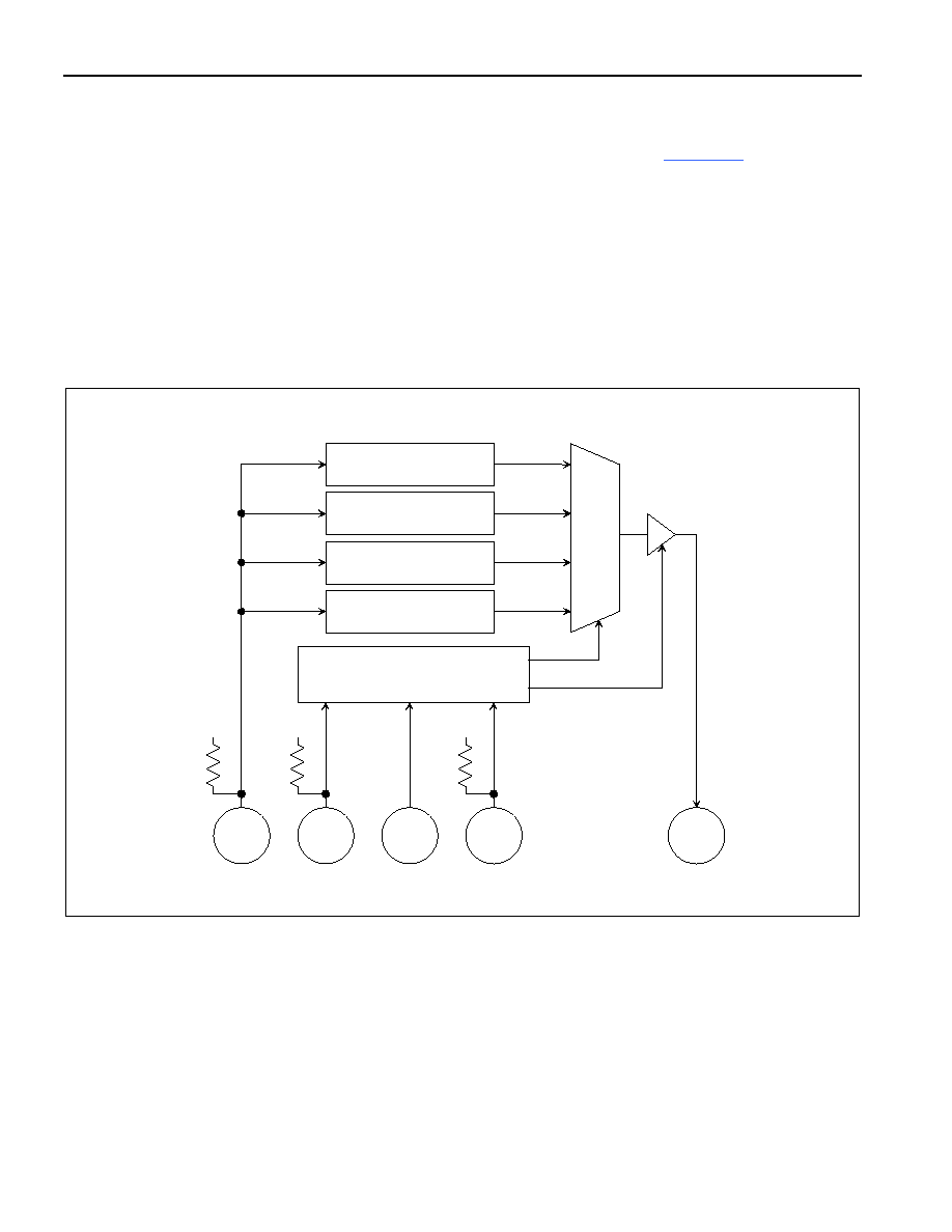
DS26102 16-Port TDM-to-ATM PHY
45 of 64
11. JTAG BOUNDARY SCAN ARCHITECTURE AND TEST ACCESS PORT
The DS26102 IEEE 1149.1 design supports the standard instruction codes SAMPLE/PRELOAD, BYPASS, and
EXTEST. Optional public instructions included are HIGHZ, CLAMP, and IDCODE (
Table 11-A
). The DS26102
contains the following functions, as required by IEEE 1149.1 Standard Test Access Port and Boundary Scan
Architecture.
Test Access Port (TAP)
TAP Controller
Instruction Register
Bypass Register
Boundary Scan Register
Device Identification Register
The TAP has the necessary interface pins JTRST, JTCLK, JTMS, JTDI, and JTDO. See the pin descriptions for
details.
Figure 11-1. JTAG Functional Block Diagram
JTDI
JTMS
JTCLK
JTRST
JTDO
TEST ACCESS PORT
CONTROLLER
V
DD
V
DD
V
DD
BOUNDRY SCAN
REGISTER
BYPASS
REGISTER
INSTRUCTION
REGISTER
IDENTIFICATION
REGISTER
MUX
SELECT
OUTPUT ENABLE
10k
10k
10k

DS26102 16-Port TDM-to-ATM PHY
46 of 64
TAP Controller State Machine. The TAP controller is a finite state machine that responds to the logic level at
JTMS on the rising edge of JTCLK (
Figure 11-2
).
Test-Logic-Reset. Upon power-up, the TAP controller is in the Test-Logic-Reset state. The instruction register
contains the IDCODE instruction. All system logic of the device operates normally.
Run-Test-Idle. The Run-Test-Idle is used between scan operations or during specific tests. The instruction register
and test registers remain idle.
Select-DR-Scan. All test registers retain their previous state. With JTMS LOW, a rising edge of JTCLK moves the
controller into the Capture-DR state and initiates a scan sequence. JTMS HIGH during a rising edge on JTCLK
moves the controller to the Select-IR-Scan state.
Capture-DR. Data can be parallel-loaded into the test data registers selected by the current instruction. If the
instruction does not call for a parallel load or the selected register does not allow parallel loads, the test register
remains at its current value. On the rising edge of JTCLK, the controller goes to the Shift-DR state if JTMS is LOW
or it goes to the Exit1-DR state if JTMS is HIGH.
Shift-DR. The test data register selected by the current instruction is connected between JTDI and JTDO and shifts
data one stage toward its serial output on each rising edge of JTCLK. If a test register selected by the current
instruction is not placed in the serial path, it maintains its previous state.
Exit1-DR. While in this state, a rising edge on JTCLK puts the controller in the Update-DR state, which terminates
the scanning process, if JTMS is HIGH. A rising edge on JTCLK with JTMS LOW puts the controller in the Pause-
DR state.
Pause-DR. Shifting of the test registers is halted while in this state. All test registers selected by the current
instruction retain their previous state. The controller remains in this state while JTMS is LOW. A rising edge on
JTCLK with JTMS HIGH puts the controller in the Exit2-DR state.
Exit2-DR. A rising edge on JTCLK with JTMS HIGH while in this state puts the controller in the Update-DR state
and terminates the scanning process. A rising edge on JTCLK with JTMS LOW enters the Shift-DR state.
Update-DR. A falling edge on JTCLK while in the Update-DR state latches the data from the shift register path of
the test registers into the data output latches. This prevents changes at the parallel output because of changes in
the shift register.
Select-IR-Scan. All test registers retain their previous state. The instruction register remains unchanged during this
state. With JTMS LOW, a rising edge on JTCLK moves the controller into the Capture-IR state and initiates a scan
sequence for the instruction register. JTMS HIGH during a rising edge on JTCLK puts the controller back into the
Test-Logic-Reset state.
Capture-IR. The Capture-IR state is used to load the shift register in the instruction register with a fixed value. This
value is loaded on the rising edge of JTCLK. If JTMS is HIGH on the rising edge of JTCLK, the controller enters the
Exit1-IR state. If JTMS is LOW on the rising edge of JTCLK, the controller enters the Shift-IR state.
Shift-IR. In this state, the shift register in the instruction register is connected between JTDI and JTDO and shifts
data one stage for every rising edge of JTCLK toward the serial output. The parallel register as well as all test
registers remains at their previous states. A rising edge on JTCLK with JTMS HIGH moves the controller to the
Exit1-IR state. A rising edge on JTCLK with JTMS LOW keeps the controller in the Shift-IR state while moving data
one stage thorough the instruction shift register.
Exit1-IR. A rising edge on JTCLK with JTMS LOW puts the controller in the Pause-IR state. If JTMS is HIGH on
the rising edge of JTCLK, the controller enters the Update-IR state and terminates the scanning process.
Pause-IR. Shifting of the instruction shift register is halted temporarily. With JTMS HIGH, a rising edge on JTCLK
puts the controller in the Exit2-IR state. The controller remains in the Pause-IR state if JTMS is LOW during a rising
edge on JTCLK.
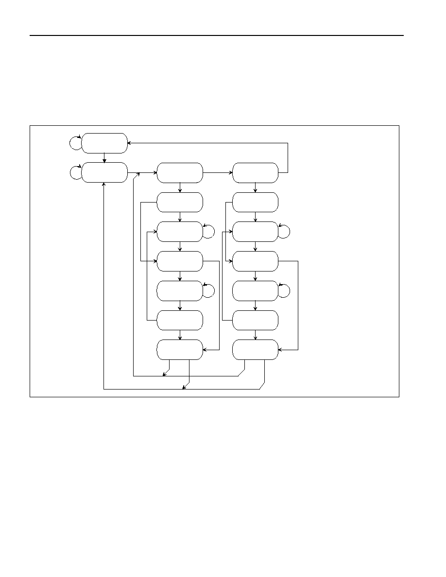
DS26102 16-Port TDM-to-ATM PHY
47 of 64
Exit2-IR. A rising edge on JTCLK with JTMS LOW puts the controller in the Update-IR state. The controller loops
back to Shift-IR if JTMS is HIGH during a rising edge of JTCLK in this state.
Update-IR. The instruction code shifted into the instruction shift register is latched into the parallel output on the
falling edge of JTCLK as the controller enters this state. Once latched, this instruction becomes the current
instruction. A rising edge on JTCLK with JTMS LOW puts the controller in the Run-Test-Idle state. With JTMS
HIGH, the controller enters the Select-DR-Scan state.
Figure 11-2. TAP Controller State Diagram
1
0
0
1
1
1
1
1
1
1
1
1
1
1
1
0
0
0
0
0
1
0
0
0
0
1
1
0
0
0
0
Select
DR-Scan
Capture DR
Shift DR
Exit DR
Pause DR
Exit2 DR
Update DR
Select
IR-Scan
Capture IR
Shift IR
Exit IR
Pause IR
Exit2 IR
Update IR
Test Logic
Reset
Run Test/
Idle
0
DS26102 16-Port TDM-to-ATM PHY
48 of 64
11.1 Instruction
Register
The instruction register contains a shift register as well as a latched parallel output and is 3 bits in length. When the
TAP controller enters the Shift-IR state, the instruction shift register is connected between JTDI and JTDO. While in
the Shift-IR state, a rising edge on JTCLK with JTMS LOW shifts the data one stage toward the serial output at
JTDO. A rising edge on JTCLK in the Exit1-IR state or the Exit2-IR state with JTMS HIGH moves the controller to
the Update-IR state. The falling edge of that same JTCLK latches the data in the instruction shift register to the
instruction parallel output. Instructions supported by the DS26102 and its respective operational binary codes are
shown in
Table 11-A
.
Table 11-A. Instruction Codes for IEEE 1149.1 Architecture
INSTRUCTION SELECTED
REGISTER INSTRUCTION
CODES
SAMPLE/PRELOAD Boundary
Scan
010
BYPASS Bypass 111
EXTEST Boundary
Scan 000
CLAMP Bypass 011
HIGHZ Bypass 100
IDCODE Device
Identification 001
SAMPLE/PRELOAD. This is a mandatory instruction for the IEEE 1149.1 specification that supports two functions.
The digital I/Os of the device can be sampled at the boundary scan register without interfering with the normal
operation of the device by using the Capture-DR state. SAMPLE/PRELOAD also allows the device to shift data into
the boundary scan register through JTDI using the Shift-DR state.
BYPASS. When the BYPASS instruction is latched into the parallel instruction register, JTDI connects to JTDO
through the 1-bit bypass test register. This allows data to pass from JTDI to JTDO without affecting the device's
normal operation.
EXTEST. This instruction allows testing of all interconnections to the device. When the EXTEST instruction is
latched in the instruction register, the following actions occur. Once enabled through the Update-IR state, the
parallel outputs of all digital output pins are driven. The boundary scan register is connected between JTDI and
JTDO. The Capture-DR samples all digital inputs into the boundary scan register.
CLAMP. All digital outputs of the device output data from the boundary scan parallel output while connecting the
bypass register between JTDI and JTDO. The outputs do not change during the CLAMP instruction.
HIGHZ. All digital outputs of the device are placed in a high-impedance state. The BYPASS register is connected
between JTDI and JTDO.
IDCODE. When the IDCODE instruction is latched into the parallel instruction register, the identification test
register is selected. The device identification code is loaded into the identification register on the rising edge of
JTCLK following entry into the Capture-DR state. Shift-DR can be used to shift the identification code out serially
through JTDO. During Test-Logic-Reset, the identification code is forced into the instruction register's parallel
output. The ID code always has a 1 in the LSB position. The next 11 bits identify the manufacturer's JEDEC
number and number of continuation bytes followed by 16 bits for the device and 4 bits for the version.
Table 11-B. ID Code Structure
MSB
LSB (Must be 1)
Version--Contact Factory
Device ID
JEDEC
1
4 Bits
See
Table 11-C
00010100001
1
Table 11-C. Device ID Codes
PART ID
CODE
DS26102 0000000000100111

DS26102 16-Port TDM-to-ATM PHY
49 of 64
11.2 Test
Registers
IEEE 1149.1 requires a minimum of two test registers--the bypass register and the boundary scan register. An
optional test register, the identification register, has been included with the DS26102 design. It is used in
conjunction with the IDCODE instruction and the Test-Logic-Reset state of the TAP controller.
Bypass Register. This is a single one-bit shift register used in conjunction with the BYPASS, CLAMP, and HIGHZ
instructions. It provides a short path between JTDI and JTDO.
Boundary Scan Register. This register contains both a shift register path and a latched parallel output for all
control cells and digital I/O cells. It is n bits in length. See
Table 11-D
for the cell bit locations and definitions.
Identification Register. The identification register contains a 32-bit shift register and a 32-bit latched parallel
output. This register is selected during the IDCODE instruction and when the TAP controller is in the Test-Logic-
Reset state.
Table 11-D. Boundary Scan Control Bits
CELL NAME
TYPE
CONTROL
CELL
0 -- controlr
1 TFP13 output3
0
2 TFP13
observe_only
3 TCLK13
observe_only
4 TDATA13 output3
161
5 -- controlr
6 TFP12 output3
5
7 TFP12
observe_only
8 TCLK12
observe_only
9 TDATA12 output3
161
10 -- controlr
11 TFP11 output3
10
12 TFP11 observe_only
13 TCLK11 observe_only
14 TDATA11 output3
161
15 -- controlr
16 TFP10 output3
15
17 TFP10 observe_only
18 TCLK10 observe_only
19 TDATA10 output3
161
20 -- controlr
21 TFP9 output3
20
22 TFP9 observe_only
23 TCLK9 observe_only
24 TDATA9 output3
161
25 -- controlr
26 TFP8 output3
25
27 TFP8 observe_only
28 TCLK8 observe_only
29 TDATA8 output3
161
30 RFP15 observe_only
31 RCLK15 observe_only
32 RDATA15 observe_only
33 RFP14 observe_only
34 RCLK14 observe_only
35 RDATA14 observe_only
36 RFP13 observe_only
37 RCLK13 observe_only
38 RDATA13 observe_only
39 RFP12 observe_only
40 RCLK12 observe_only
CELL NAME
TYPE
CONTROL
CELL
41 RDATA12 observe_only
42 RFP11 observe_only
43 RCLK11 observe_only
44 RDATA11 observe_only
45 RFP10 observe_only
46 RCLK10 observe_only
47 RDATA10 observe_only
48 RFP9 observe_only
49 RCLK9 observe_only
50 RDATA9 observe_only
51 RFP8 observe_only
52 RCLK8 observe_only
53 RDATA8 observe_only
54 RLCD15 output3
161
55 RLCD14 output3
161
56 RLCD13 output3
161
57 RLCD12 output3
161
58 RLCD11 output3
161
59 RLCD10 output3
161
60 RLCD9 output3
161
61 RLCD8 output3
161
62 RLCD7 output3
161
63 RLCD6 output3
161
64 RLCD5 output3
161
65 RLCD4 output3
161
66 RLCD3 output3
161
67 RLCD2 output3
161
68 RLCD1 output3
161
69 RLCD0 output3
161
70 UR_PAR output3
77
71 UR_CLAV3 output3
73
72 UR_CLAV2 output3
73
73 -- controlr
74 UR_CLAV1 output3
73
75 -- controlr
76 UR_CLAV0 output3
75
77 -- controlr
78 UR_SOC output3
77
79 UR_DATA0 output3
86
80 UR_DATA1 output3
86
81 UR_DATA2 output3
86

DS26102 16-Port TDM-to-ATM PHY
50 of 64
CELL NAME
TYPE
CONTROL
CELL
82 UR_DATA3 output3
86
83 UR_DATA4 output3
86
84 UR_DATA5 output3
86
85 UR_DATA6 output3
86
86 -- controlr
87 UR_DATA7 output3
86
88 UR_CLK observe_only
89
UR_ENB
observe_only
90 UR_ADDR0 observe_only
91 UR_ADDR1 observe_only
92 UR_ADDR2 observe_only
93 UR_ADDR3 observe_only
94 UR_ADDR4 observe_only
95 UT_2CLAV3 output3
100
96 UT_2CLAV2 output3
100
97 UT_2CLAV1 output3
100
98 UT_CLAV3 output3
100
99 UT_CLAV2 output3
100
100 --
controlr
101 UT_CLAV1
output3
100
102 UT_2CLAV0
output3
103
103 --
controlr
104 UT_CLAV0
output3
103
105 UT_PAR observe_only
106 UT_CLK observe_only
107 UT_SOC observe_only
108 UT_DATA0 observe_only
109 UT_DATA1 observe_only
110 UT_DATA2 observe_only
111 UT_DATA3 observe_only
112 UT_DATA4 observe_only
113 UT_DATA5 observe_only
114 UT_DATA6 observe_only
115 UT_DATA7 observe_only
116
UT_ENB
observe_only
117 UT_ADDR0 observe_only
118 UT_ADDR1 observe_only
119 UT_ADDR2 observe_only
120 UT_ADDR3 observe_only
121 UT_ADDR4 observe_only
122 --
controlr
123 TFP7
output3
122
124 TFP7 observe_only
125 TCLK7 observe_only
126 TDATA7
output3
161
127 --
controlr
128 TFP6
output3
127
129 TFP6 observe_only
130 TCLK6 observe_only
131 TDATA6
output3
161
132 --
controlr
133 TFP5
output3
132
134 TFP5 observe_only
135 TCLK5 observe_only
136 TDATA5
output3
161
137 --
controlr
138 TFP4
output3
137
139 TFP4 observe_only
140 TCLK4 observe_only
CELL NAME
TYPE
CONTROL
CELL
141 TDATA4
output3
161
142 --
controlr
143 TFP3
output3
142
144 TFP3 observe_only
145 TCLK3 observe_only
146 TDATA3
output3
161
147 --
controlr
148 TFP2
output3
147
149 TFP2 observe_only
150 TCLK2 observe_only
151 TDATA2
output3
161
152 --
controlr
153 TFP1
output3
152
154 TFP1 observe_only
155 TCLK1 observe_only
156 TDATA1
output3
161
157 --
controlr
158 TFP0
output3
157
159 TFP0 observe_only
160 TCLK0 observe_only
161 --
controlr
162 TDATA0
output3
161
163 RFP7 observe_only
164 RCLK7 observe_only
165 RDATA7 observe_only
166 RFP6 observe_only
167 RCLK6 observe_only
168 RDATA6 observe_only
169 RFP5 observe_only
170 RCLK5 observe_only
171 RDATA5 observe_only
172 RFP4 observe_only
173 RCLK4 observe_only
174 RDATA4 observe_only
175 RFP3 observe_only
176 RCLK3 observe_only
177 RDATA3 observe_only
178 RFP2 observe_only
179 RCLK2 observe_only
180 RDATA2 observe_only
181 RFP1 observe_only
182 RCLK1 observe_only
183 RDATA1 observe_only
184 RFP0 observe_only
185 RCLK0 observe_only
186 RDATA0 observe_only
187
INT
output2 187
188 --
internal
189
INT
observe_only
190 BLS0 observe_only
191 MUX observe_only
192 BTS observe_only
193
CS
observe_only
194
WR (R/W)
observe_only
195
RD (DS)
observe_only
196 D0/AD0
output3
210
197 D0/AD0 observe_only
198 D1/AD1
output3
210
199 D1/AD1 observe_only

DS26102 16-Port TDM-to-ATM PHY
51 of 64
CELL NAME
TYPE
CONTROL
CELL
200 D2/AD2
output3
210
201 D2/AD2 observe_only
202 D3/AD3
output3
210
203 D3/AD3 observe_only
204 D4/AD4
output3
210
205 D4/AD4 observe_only
206 D5/AD5
output3
210
207 D5/AD5 observe_only
208 D6/AD6
output3
210
209 D6/AD6 observe_only
210 --
controlr
211 D7/AD7
output3
210
212 D7/AD7 observe_only
213 A0 observe_only
214 A1 observe_only
215 A2 observe_only
216 A3 observe_only
217 A4 observe_only
218 A5 observe_only
219 A6 observe_only
220 A7/ALE
(AS) observe_only
221 EXSTAT7 observe_only
222 EXSTAT6 observe_only
CELL NAME
TYPE
CONTROL
CELL
223 EXSTAT5 observe_only
224 EXSTAT4 observe_only
225 EXSTAT3 observe_only
226 EXSTAT2 observe_only
227 EXSTAT1 observe_only
228 EXSTAT0 observe_only
229 1SECOUT
output3
161
230 8KHZIN observe_only
231 GCLKIN observe_only
232 GCLKOUT
output3
161
233 REFCLKIN observe_only
234
RESET
observe_only
235 --
controlr
236 TFP15
output3
235
237 TFP15 observe_only
238 TCLK15 observe_only
239 TDATA15
output3
161
240 --
controlr
241 TFP14
output3
240
242 TFP14 observe_only
243 TCLK14 observe_only
244 TDATA14
output3
161
DS26102 16-Port TDM-to-ATM PHY
52 of 64
12. OPERATING
PARAMETERS
ABSOLUTE MAXIMUM RATINGS
Voltage Range on Any Pin with Respect to V
SS
(except V
DD
)
-0.3V to +5.5V
Supply Voltage (V
DD
) Range with Respect to V
SS
-0.3V to +3.63V
Operating Temperature Range
-40ºC to +85ºC
Storage Temperature Range
-55ºC to +125ºC
Soldering Temperature
See IPC/JEDEC J-STD-020A
Stresses beyond those listed under "Absolute Maximum Ratings" may cause permanent damage to the device. These are stress ratings only,
and functional operation of the device at these or any other conditions beyond those indicated in the operational sections of the specifications is
not implied. Exposure to the absolute maximum rating conditions for extended periods may affect device.
RECOMMENDED DC OPERATING CONDITIONS
(T
A
= -40ºC to +85ºC)
PARAMETER SYMBOL
MIN
TYP
MAX
UNITS
Logic 1
V
IH
2.0 5.5
V
Logic 0
V
IL
-0.3 +0.8
V
Supply V
DD
3.135
3.3
3.465
V
CAPACITANCE
(T
A
= +25ºC)
PARAMETER SYMBOL
MIN
TYP
MAX
UNITS
Input Capacitance
C
IN
7
pF
Output Capacitance
C
OUT
7
pF
DC CHARACTERISTICS
(V
DD
= 3.135V to 3.465V, T
A
= -40°C to +85°C.)
PARAMETER SYMBOL
MIN
TYP
MAX
UNITS
Supply Current at 3.3V (Note 2)
I
DD
85
mA
Input Leakage
I
IL
-10.0
+10.0
µA
Tri-State Output Leakage
I
OL
-10.0
+10.0
µA
Output Voltage (I
o
= -4.0mA) (Note 3)
V
OH
2.4 V
Output Voltage (I
o
= +4.0mA) (Note 3)
V
OL
0.4
V
UTOPIA V
OH
(I
o
= -8.0mA) (Note 4)
V
OHU
2.4 V
UTOPIA V
OL
(I
o
= +8.0mA) (Note 4)
V
OLU
0.4
V
Note 1: Theta-Ja is based on the package mounted on a 4-layer JEDEC board and measured in a JEDEC test chamber.
Note 2: RCLK1 - n = TCLK1 - n = 2.048MHz, GCLK = 32.768MHz.
Note 3: Applies to all non-UTOPIA outputs.
Note 4: Applies to UTOPIA outputs.
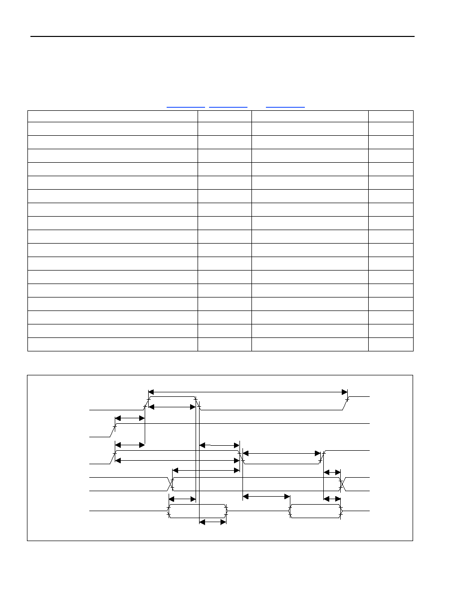
DS26102 16-Port TDM-to-ATM PHY
53 of 64
13. CRITICAL TIMING INFORMATION
Unless otherwise noted, all timing numbers assume 20pF test load on output signals, 40pF test load on bus
signals.
Table 13-A. AC Characteristics--Multiplexed Parallel Port (MUX = 1)
(V
DD
= 3.3V
±5%, T
A
= -40°C to +85°C.) (
Figure 13-1
,
Figure 13-2
, and
Figure 13-3
)
PARAMETER SYMBOL
MIN
TYP
MAX
UNITS
Cycle Time
t
CYC
200 ns
Pulse Width, DS Low or RD High
PW
EL
100 ns
Pulse Width, DS High or RD Low
PW
EH
100 ns
Input Rise/Fall Times
t
R
, t
F
20
ns
R/W Hold Time
t
RWH
10 ns
R/W Setup Time Before DS High
t
RWS
50 ns
CS Setup Time Before DS, WR, or RD Active
t
CS
20 ns
CS Hold Time
t
CH
0 ns
Read Data Hold Time
t
DHR
10 50
ns
Write Data Hold Time
t
DHW
5 ns
Muxed Address Valid to AS or ALE Fall
t
ASL
15 ns
Muxed Address Hold Time
t
AHL
10 ns
Delay Time DS, WR, or RD to AS or ALE Rise
t
ASD
20 ns
Pulse Width AS or ALE High
PW
ASH
30 ns
Delay Time, AS or ALE to DS,
WR, or RD
t
ASED
10 ns
Output Data Delay Time from DS or RD
t
DDR
80
ns
Data Setup Time
t
DSW
50 ns
Figure 13-1. Intel Bus Read Timing (BTS = 0/MUX = 1)
ASH
PW
tCYC
tASD
tASD
PW
PW
EH
EL
t
t
t
t
t
t
AHL
CH
CS
ASL
ASED
CS_B
AD0-AD7
DHR
t DDR
ALE (A7)
RD_B
WR_B
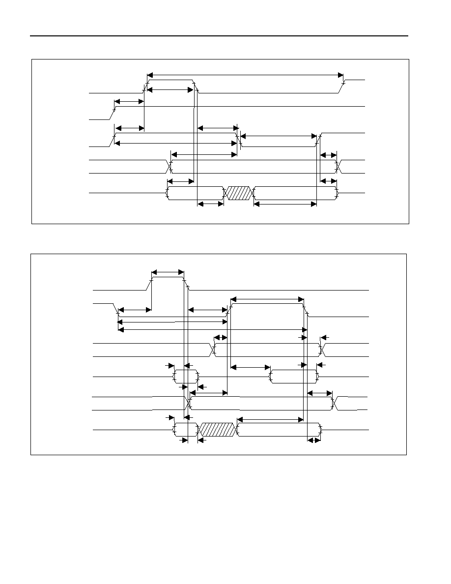
DS26102 16-Port TDM-to-ATM PHY
54 of 64
Figure 13-2. Intel Bus Write Timing (BTS = 0/MUX = 1)
Figure 13-3. Motorola Bus Timing (BTS = 1/MUX = 1)
ASH
PW
tCYC
tASD
t ASD
PW
PW
EH
EL
t
t
t
t
t
t
t
AHL
DSW
DHW
CH
CS
ASL
ASED
CS_B
AD0-AD7
RD_B
WR_B
ALE (A7)
t
ASD
ASH
PW
t
t
ASL
AHL
t CS
t
ASL
t
t
t
DSW
DHW
t CH
t
t
t
DDR
DHR
RWH
t ASED
PW
EH
t RWS
AHL
PW
EL
t CYC
AS
DS
AD0-AD7
(WRITE)
AD0-AD7
(READ)
R/
W
CS_B
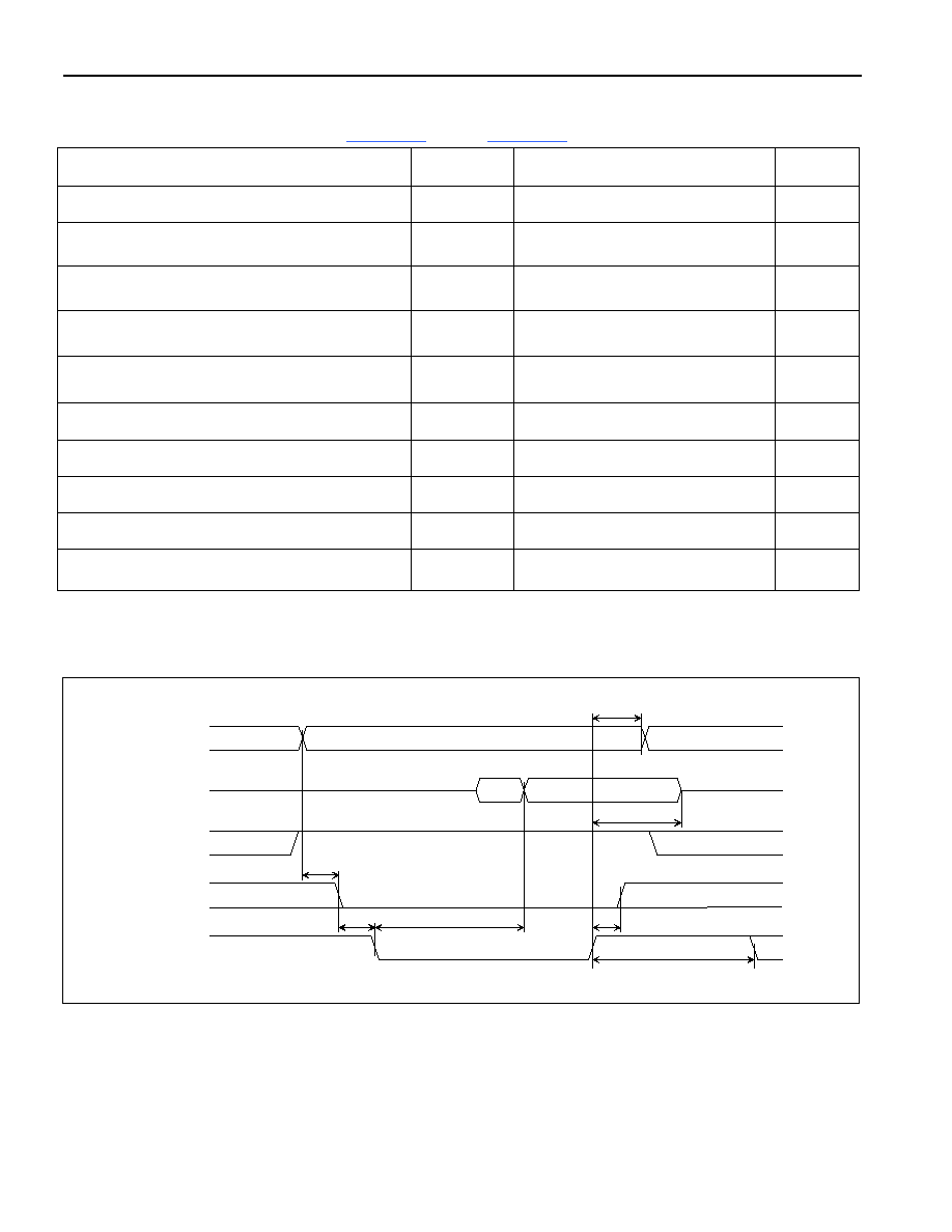
DS26102 16-Port TDM-to-ATM PHY
55 of 64
Table 13-B. AC Characteristics--Nonmultiplexed Parallel Port (MUX = 1)
(V
DD
= 3.3V
±5%, T
A
= -40°C to +85°C.) (
Figure 13-4
through
Figure 13-7
)
PARAMETER SYMBOL
MIN
TYP
MAX
UNITS
Setup Time for A[7:0], BLS0 Valid to CS Active
t1 0
ns
Setup Time for CS Active to Either RD or WR
Active
t2 0
ns
Delay Time from Either RD or DS Active to
D/AD[7:0] Valid
t3
130
ns
Hold Time from Either RD or WR Inactive to CS
Inactive
t4 0
ns
Hold Time from CS or RD or DS Inactive to
D/AD[7:0] Tri-State
t5 5
25
ns
Wait Time from WR Active to Latch Data
t6 30 ns
Data Setup Time to WR Inactive
t7 10 ns
Data Hold Time from WR Inactive
t8 2
ns
Address, BLS0 Hold from WR Inactive
t9 0
ns
Write Access to Subsequent Write/Read Access
Delay Time (Note 1)
t10
5 x GCLK
ns
Note 1: Time t10 should be minimum 5 x the GCLKIN period. For a GCLKIN = 33MHz, t10 = 150ns.
Note 2: Interrupt is deasserted at 5 x GCLKIN period + 40ns maximum from
RD active.
Figure 13-4. Intel Bus Read Timing (BTS = 0/MUX = 0)
t2
t3
ADDRESS VALID
DATA VALID
t4
t9
t5
t10
ADDR[7:0]
DATA[7:0]
CS_B
RD_B
WR_B
t1
DS26102 16-Port TDM-to-ATM PHY
56 of 64
Figure 13-5. Intel Bus Write Timing (BTS = 0/MUX = 0)
Figure 13-6. Motorola Bus Read Timing (BTS = 1/MUX = 0)
Figure 13-7. Motorola Bus Write Timing (BTS = 1/MUX = 0)
t2
t6
ADDRESS VALID
t4
t9
t10
ADDR[7:0]
DATA[7:0]
CS_B
RD_B
WR_B
t7
t8
t1
t2
t3
ADDRESS VALID
DATA VALID
t4
t9
t5
t10
ADDR[7:0]
DATA[7:0]
CS_B
DS_B
R/W_B
t1
t2
t6
ADDRESS VALID
t4
t10
ADDR[7:0]
DATA[7:0]
CS_B
R/W_B
DS_B
t7
t8
t1
t9

DS26102 16-Port TDM-to-ATM PHY
57 of 64
Table 13-C. Framer Interface AC Characteristics
PARAMETER SYMBOL
MIN
TYP
MAX
UNITS
RCLK
Duty
Cycle
30 70 %
RDATA and RFP Setup to RCLK Active Edge
t11
10
ns
RDATA and RFP Hold from RCLK Active Edge
t12
2
ns
TCLK Duty Cycle
30
70
%
Output Delay TDATA and TFP from TCLK Active
Edge (Note 3)
t13
20
ns
TFP Setup Time to TCLK Active Edge (Note 4)
t14
10
ns
TFP Hold Time from TCLK Active Edge (Note 4)
t15
10
ns
Note 3: TFP is an output.
Note 4: TFP is an input.
Table 13-D. UTOPIA Transmit AC Characteristics
PARAMETER SYMBOL
MIN
TYP
MAX
UNITS
UT_CLK Frequency
0
25
MHz
UT_CLK Duty Cycle
40
60
%
Setup Time UT_DATA[x], UT_ADDR[x], UT_ENB,
UT_SOC, UT_PAR inputs to UT_CLK
t20 (ts)
10
ns
Hold Time UT_DATA[x], UT_ADDR[x], UT_ENB,
UT_SOC, UT_PAR Inputs from UT_CLK
t21 (th)
1
ns
Output Delay UT_CLAV[x] from UT_CLK
t22 (td)
20
ns
Output Tri-State Delay UT_CLAV[x] from UT_CLK
t23 (tz)
25
ns
Table 13-E. UTOPIA Receive AC Characteristics
PARAMETER SYMBOL
MIN
TYP
MAX
UNITS
UR_CLK Frequency
0
25
MHz
UR_CLK
Duty
Cycle
40 60 %
Setup Time UR_ADDR[x] and UR_ENB Inputs to
UR_CLK
t24 (ts)
10
ns
Hold Time UR_ADDR[x] and UR_ENB Inputs from
UR_CLK
t25 (th)
1
ns
Output Delay UR_CLAV[x], UR_DATA[x],
UR_SOC, and UR_PAR from UR_CLK
t26 (td)
20
ns
Output Tri-State Delay UR_CLAV[x], UR_DATA[x],
UR_SOC, and UR_PAR from UR_CLK
t27 (tz)
25
ns
DS26102 16-Port TDM-to-ATM PHY
58 of 64
Figure 13-8. Setup/Hold Time Definition
Figure 13-9. Delay Time Definition
Table 13-F. JTAG Interface Timing
(V
DD
= 3.3V
±5%, T
A
= -40°C to +85°C.) (
Figure 13-10
)
PARAMETER SYMBOL
MIN
TYP
MAX
UNITS
JTCLK Clock Period
t1
1000
ns
JTCLK Clock High/Low Time (Note 5)
t2/t3
50
500
ns
JTCLK to JTDI, JTMS Setup Time
t4
3
ns
JTCLK to JTDI, JTMS Hold Time
t5
2
ns
JTCLK to JTDO Delay
t6
2
50
ns
JTCLK to JTDO High-Z Delay
t7
2
50
ns
JTRST Width Low Time
t8 100 ns
Note 5: Clock can be stopped high or low.
Figure 13-10. JTAG Interface Timing Diagram
CLOCK
SIGNAL
ts
th
INPUT SETUP TO CLOCK
INPUT HOLD FROM CLOCK
CLOCK
SIGNAL
td AND tz
JTCLK
t1
JTD0
t4
t5
t2
t3
t7
JTDI, JTMS,
JTRST
t6
JTRST
t8
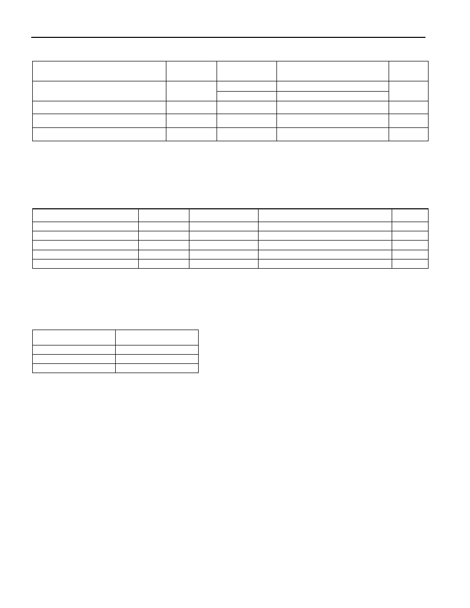
DS26102 16-Port TDM-to-ATM PHY
59 of 64
Table 13-G. System Clock AC Characteristics
PARAMETER
SYMBOL
CONDITIONS MIN TYP MAX UNITS
1.544
REFCLKIN Frequency
2.048
MHz
REFCLKIN Duty Cycle
40
60
%
GCLK Frequency
(Note 6)
16
40
MHz
GCLK
Duty
Cycle
40 60 %
Note 6: GCLK frequency must be at least 10 times the line rate (either 1.544MHz or 2.048MHz).
14. THERMAL
INFORMATION
Table 14-A. Thermal Properties, Natural Convection
PARAMETER SYMBOL
CONDITIONS
MIN
TYP
MAX
UNITS
Ambient Temperature
(Note 1)
-40°C
+85°C
Junction Temperature
-40°C
+125°C
Theta-JA (
q
JA
), Still Air
(Note
2)
20.27°C/W
Psi-JB
8.27°C/W
Psi-JT
0.24°C/W
Note 1: The package is mounted on a 4-layer JEDEC standard test board with no airflow and dissipating maximum power.
Note 2: Theta-JA (
q
JA
) is the junction to ambient thermal resistance, when the package is mounted on a 4-layer JEDEC standard test board with
no airflow and dissipating maximum power.
Table 14-B. Theta-JA (
q
JA
) vs. Airflow
FORCED AIR (m/s)
THETA-JA (
q
JA
)
0 20.27°C/W
1 17.44°C/W
2.5 16.18°C/W
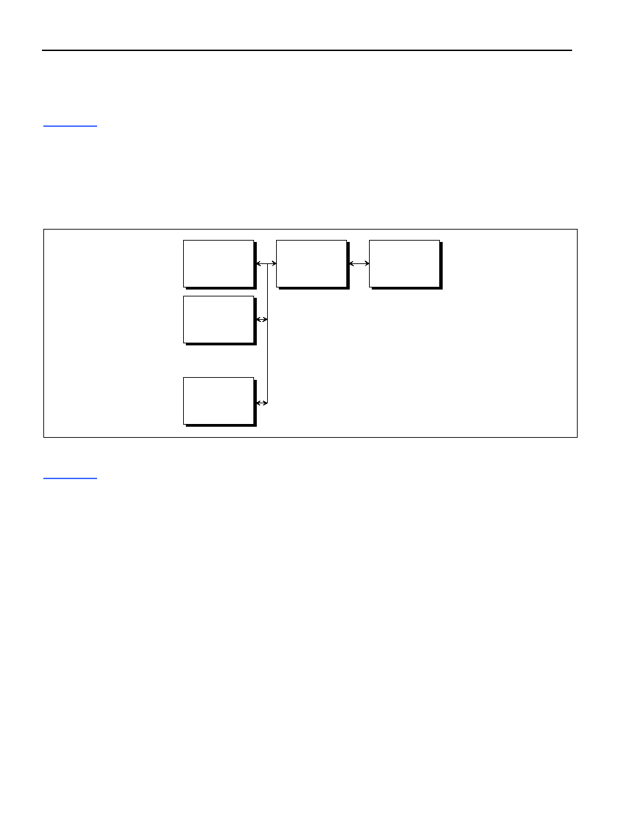
DS26102 16-Port TDM-to-ATM PHY
60 of 64
15. APPLICATIONS
INFORMATION
15.1 Application in ATM User-Network Interfaces
Figure 15-1
shows the application of the DS26102 in an ATM user-network interface (UNI). In a UNI, the DS26102
provides the transmission convergence sublayer functionality. The interface between the DS26102 and the ATM
layer is governed by UTOPIA II specification from the ATM forum. Multiplexing with 1CLAV can be used as
UTOPIA polling mode. The DS26102 supports up to 16 T1/E1 ports. For cell-rate decoupling, 4-cell buffer is
allocated per port separately in the transmit and receive interfaces with the ATM layer. The buffer size of the
transmit FIFO is configurable to 2, 3, or 4 cells. This flexibility in changing the FIFO depth provides users the
control over cell latency, if desired.
Figure 15-1. User-Network Interface Application
15.2 Interfacing with Framers
Figure 15-2
shows two methods of interfacing the DS26102 to a Dallas framer. One method shows a "loop timing"
method where TCLK, TSYNC/TFPx, RFPx, and RCLK are derived from the receive framer's RCLK and RSYNC.
The other method shows an interface where transmit and receive are independent.
The following guidelines are suggested:
§
TCLK may be derived from RCLK. TCLK must be 1.544MHz for T1 and 2.048MHz for E1.
§
The framer elastic stores should be disabled on both transmit and receive sides.
§
RSYNC must be configured as a frame-boundary output.
§
The framer TSYNC can be an input or an output (the DS26102 must be programmed accordingly). TSYNC
should be configured for frame-boundary mode.
§
The TSYNC and RSYNC signals should be high for only one TCLK and RCLK period, respectively.
ATM
LAYER
DS26102
T1/E1
FRAMER
1
T1/E1
FRAMER
2
T1/E1
FRAMER
16
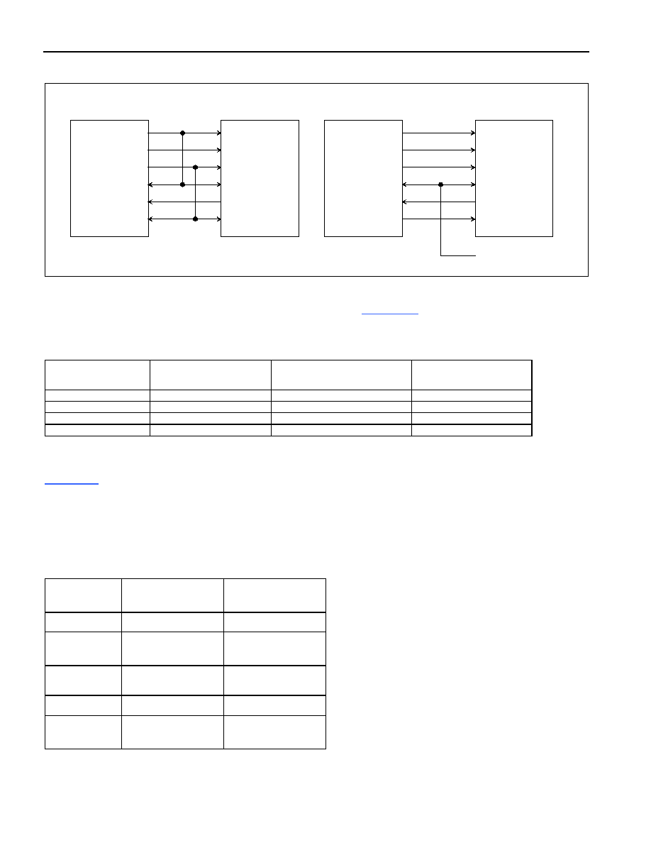
DS26102 16-Port TDM-to-ATM PHY
61 of 64
Figure 15-2. DS26102 Interfacing with Dallas Framer in Framing-Pulse Mode
When interfacing to framers where the framing pulse and data-active edge are individually configurable, ensure
that the sampling and updating happen in opposite edges.
Table 15-A
demonstrates the recommended
configurations for interfacing the DS26102 to the framer signals.
Table 15-A. Suggested Clock Edge Configurations
DATA UPDATE
EDGE IN DS26102
DATA-SAMPLING
EDGE IN FRAMER
FRAMING-PULSE
DIRECTION
FRAMING-PULSE
EDGE IN FRAMER
Positive
Negative
From DS26102 to framer
Negative for sampling
Negative
Positive
From DS26102 to framer
Positive for sampling
Positive
Negative
From framer to DS26102
Positive for updating
Negative
Positive
From framer to DS26102
Negative for updating
15.3 Fractional T1/E1 Support
Table 15-B
describes the configuration needed by the DS26102 for supporting fractional T1/E1. Note that in E1
mode, the DS26102 must be used in gapped-clock mode, where the clock is gapped during inactive channels as
well as TS0 and TS16 for CAS-framed format. When configured for T1, either frame-pulse or gapped-clock mode
can be used, however, the TFP and RFP signals must be generated during framing overhead-bit and nonactive-
DS0/TS positions of the T1 frame. Older Dallas framers may require additional logic to implement gapped-clock
operation.
Table 15-B. Fractional T1/E1 Register Settings
CONTROL
REGISTER
BIT
T1 E1
TPC 0
1
TPLIM
0 for frame-pulse
mode or 1 for
gapped-clock mode
1 (gapped-clock
mode only)
TFSD
0 (input only)
0 for TFP as input or
1 for TFP as output
RPC 0
1
RPLIM
0 for frame-pulse
mode or 1 for
gapped-clock mode
1 (gapped-clock
mode only)
DS26102
RCLKx
RDATAx
RFPx
TCLKx
TDATAx
TFPx
DALLAS
FRAMER
RCLK
RSER
RSYNC
TSER
TCLK
TSYNC
DS26102
RCLKx
RDATAx
RFPx
TCLKx
TDATAx
TFPx
DALLAS
FRAMER
RCLK
RSER
RSYNC
TSER
TCLK
TSYNC
CLOCK
x = 0 - 15
x = 0 - 15
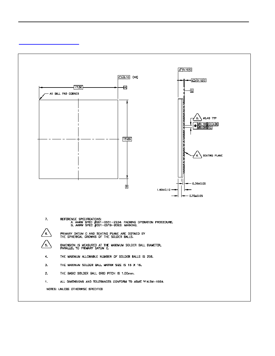
DS26102 16-Port TDM-to-ATM PHY
62 of 64
16. PACKAGE
INFORMATION
(The package drawing(s) in this data sheet may not reflect the most current specifications. For the latest package outline information, go to
www.maxim-ic.com/DallasPackInfo
.)
Note: All dimensions in millimeters.
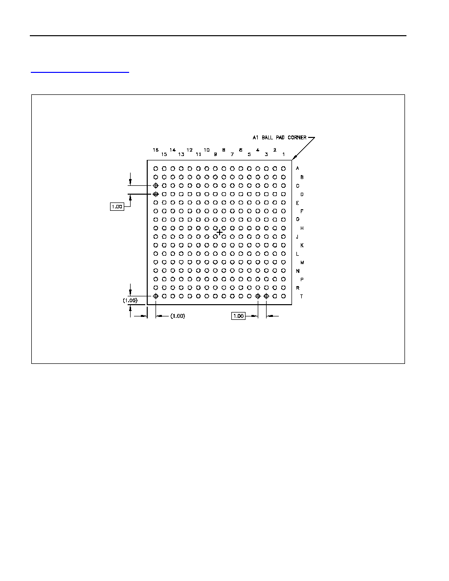
DS26102 16-Port TDM-to-ATM PHY
63 of 64
PACKAGE INFORMATION (continued)
(The package drawing(s) in this data sheet may not reflect the most current specifications. For the latest package outline information, go to
www.maxim-ic.com/DallasPackInfo
.)
Bottom Mechanical Dimensions
Note: All dimensions in millimeters.

DS26102 16-Port TDM-to-ATM PHY
64 of 64
17. REVISION
HISTORY
REVISION DESCRIPTION
021403
New product release
Document Outline