 | –≠–ª–µ–∫—Ç—Ä–æ–Ω–Ω—ã–π –∫–æ–º–ø–æ–Ω–µ–Ω—Ç: DS26324 | –°–∫–∞—á–∞—Ç—å:  PDF PDF  ZIP ZIP |

1 of 112
REV: 070105
Note: Some revisions of this device may incorporate deviations from published specifications known as errata. Multiple revisions of any device
may be simultaneously available through various sales channels. For information about device errata, click here:
www.maxim-ic.com/errata
.
GENERAL DESCRIPTION
The DS26324 is a 16-channel short-haul line
interface unit (LIU) that supports E1/T1/J1 from a
single 3.3V power supply. A wide variety of
applications are supported through internal
impedance matching. A single bill of material can
support E1/T1/J1 with minimum external
components. Redundancy is supported through
nonintrusive monitoring, optimal high-impedance
modes, and configurable 1:1 or 1+1 backup
enhancements. An on-chip synthesizer generates the
E1/T1/J1 clock rates by a single master clock input of
various frequencies. Two clock output references are
also offered. The device is offered a 256-pin TEBGA,
the smallest package available for a 16-channel LIU.
APPLICATIONS
T1 Digital Cross-Connects
ATM and Frame Relay Equipment
Wireless Base Stations
ISDN Primary Rate Interface
E1/T1/J1 Multiplexer and Channel Banks
E1/T1/J1 LAN/WAN Routers
FUNCTIONAL DIAGRAM
TNEG
RCLK
TPOS
TCLK
RPOS
RNEG
SOFTWARE CONTROL
AND JTAG
TRANSMITTER
RECEIVER
LOSS
1
16
RTIP
RRING
JTAG
TTIP
TRING
FEATURES
ß
16 E1, T1, or J1 Short-Haul Line Interface Units
ß
Independent E1, T1, or J1 selections
ß
Software-Selectable Transmit and Receive-Side
Impedance Matching
ß
Crystal Less Jitter Attenuator
ß
Selectable Single-Rail and Dual-Rail Mode and
AMI or HDB3/ B8ZS Line Encoding and
Decoding
ß
Detection and Generation of AIS
ß
Digital/Analog Loss of Signal Detection as per
T1.231, G.775, and ETSI 300233
ß
External Master Clock can be Multiple of 2.048 or
1.544MHz for T1/J1 or E1 Operation (This clock
will be internally adapted for T1 or E1 Use.)
ß
Receiver Signal Level Indicator from -2.5dB to
-20dB in 2.5dB Increments
ß
Two Built-In BERT Testers for Diagnostics
ß
8-Bit Parallel Interface Support for Intel or
Motorola Mode, or 4-Wire Serial Interface
ß
Transmit Short-Circuit Protection
ß
G.772 Nonintrusive Monitoring
ß
Receive Monitor Mode Handles Combinations of
14dB or 20dB of Resistive Attenuation Along with
12dB to 30dB of Cable Attenuation.
ß
Specification Compliance to the Latest T1/E1
Standards--ANSI T1.102, AT&T Pub 62411,
T1.231, T1.403, ITU G.703, G.742, G.775,
G.823, ETSI 300 166, and ETSI 300 233
ß
Single 3.3V Supply with 5V Tolerant I/O
ß
JTAG Boundary Scan as per IEEE 1149.1
ORDERING INFORMATION
PART TEMP
RANGE
PIN-PACKAGE
DS26324G
0∞C to +70∞C
256 TEBGA
DS26324GN
-40∞C to +85∞C 256 TEBGA
DS26324
3.3V, 16-Channel, E1/T1/J1
Short-Haul Line Interface Unit
www.maxim-ic.com

DS26324 3.3V, 16-Channel, E1/T1/J1, Short-Haul Line Interface Unit
2 of 112
TABLE OF CONTENTS
1
STANDARDS COMPLIANCE ........................................................................................................ 6
1.1
T
ELECOM
S
PECIFICATIONS
C
OMPLIANCE
.......................................................................................................... 6
2
DETAILED DESCRIPTION............................................................................................................. 7
3
BLOCK DIAGRAMS....................................................................................................................... 8
4
PIN DESCRIPTION ...................................................................................................................... 10
5
FUNCTIONAL DESCRIPTION ..................................................................................................... 18
5.1
P
ORT
O
PERATION
......................................................................................................................................... 18
5.1.1
Serial Port Operation .......................................................................................................................... 18
5.1.2
Parallel Port Operation........................................................................................................................ 19
5.1.3
Interrupt Handling................................................................................................................................ 19
5.2
P
OWER
-U
P AND
R
ESET
................................................................................................................................. 20
5.3
M
ASTER CLOCK
............................................................................................................................................. 20
5.4
T
RANSMITTER
............................................................................................................................................... 21
5.4.1
Transmit Line Templates .................................................................................................................... 23
5.4.2
LIU Transmit Front End....................................................................................................................... 26
5.4.3
Dual Rail.............................................................................................................................................. 27
5.4.4
Single-Rail Mode................................................................................................................................. 27
5.4.5
Zero Suppression--B8ZS or HDB3 .................................................................................................... 27
5.4.6
Transmit Power-Down ........................................................................................................................ 27
5.4.7
Transmit All Ones................................................................................................................................ 28
5.4.8
Drive Failure Monitor........................................................................................................................... 28
5.5
R
ECEIVER
..................................................................................................................................................... 28
5.5.1
Receiver Monitor Mode....................................................................................................................... 28
5.5.2
Peak Detector and Slicer .................................................................................................................... 28
5.5.3
Receive Level Indicator....................................................................................................................... 28
5.5.4
Clock and Data Recovery ................................................................................................................... 29
5.5.5
Loss of Signal...................................................................................................................................... 29
5.5.6
AIS ...................................................................................................................................................... 30
5.5.7
Bipolar Violation and Excessive Zero detector ................................................................................... 31
5.6
J
ITTER
A
TTENUATOR
..................................................................................................................................... 31
5.7
G.772 M
ONITOR
........................................................................................................................................... 32
5.8
L
OOPBACKS
.................................................................................................................................................. 32
5.8.1
Analog Loopback ................................................................................................................................ 32
5.8.2
Digital Loopback.................................................................................................................................. 33
5.8.3
Remote Loopback ............................................................................................................................... 34
5.9
BERT........................................................................................................................................................... 34
5.9.1
General Description ............................................................................................................................ 34
5.9.2
Configuration and Monitoring.............................................................................................................. 35
5.9.3
Receive Pattern Detection .................................................................................................................. 36
5.9.4
Transmit Pattern Generation............................................................................................................... 38
6
REGISTER MAPS AND DEFINITION .......................................................................................... 39
6.1
R
EGISTER
D
ESCRIPTION
................................................................................................................................ 48
6.1.1
Primary Register Bank ........................................................................................................................ 48
6.1.2
Secondary Register Bank ................................................................................................................... 60
6.1.3
Individual LIU Register Bank............................................................................................................... 62
6.1.4
BERT Registers .................................................................................................................................. 78
7
JTAG-BOUNDARY-SCAN ARCHITECTURE AND TEST-ACCESS PORT ................................. 85
7.1
TAP C
ONTROLLER
S
TATE
M
ACHINE
............................................................................................................... 86
7.2
I
NSTRUCTION
R
EGISTER
................................................................................................................................ 89
7.3
T
EST
R
EGISTERS
........................................................................................................................................... 90
7.4
B
OUNDARY
S
CAN
R
EGISTER
.......................................................................................................................... 90
7.5
B
YPASS
R
EGISTER
........................................................................................................................................ 90

DS26324 3.3V, 16-Channel, E1/T1/J1, Short-Haul Line Interface Unit
3 of 112
7.6
I
DENTIFICATION
R
EGISTER
............................................................................................................................. 90
8
DC ELECTRICAL CHARACTERIZATION ................................................................................... 91
9
AC TIMING CHARACTERISTICS ................................................................................................ 92
9.1
L
INE
I
NTERFACE
C
HARACTERISTICS
............................................................................................................... 92
9.2
P
ARALLEL
H
OST
I
NTERFACE
T
IMING
C
HARACTERISTICS
.................................................................................. 93
9.3
S
ERIAL
P
ORT
.............................................................................................................................................. 105
9.4
S
YSTEM
T
IMING
........................................................................................................................................... 106
9.5
JTAG T
IMING
.............................................................................................................................................. 108
10
PIN CONFIGURATION............................................................................................................... 109
11
PACKAGE INFORMATION........................................................................................................ 110
12
THERMAL INFORMATION ........................................................................................................ 111
13
REVISION HISTORY.................................................................................................................. 112

DS26324 3.3V, 16-Channel, E1/T1/J1, Short-Haul Line Interface Unit
4 of 112
LIST OF FIGURES
Figure 3-1. Block Diagram ........................................................................................................................................... 8
Figure 3-2. Receive Logic Detail.................................................................................................................................. 9
Figure 3-3. Transmit Logic Detail................................................................................................................................. 9
Figure 5-1. Serial Port Operation for Write Access ................................................................................................... 18
Figure 5-2. Serial Port Operation for Read Access with CLKE = 0 ........................................................................... 18
Figure 5-3. Serial Port Operation for Read Access with CLKE = 1 ........................................................................... 19
Figure 5-4. Interrupt Handling Flow Diagram ............................................................................................................ 20
Figure 5-5. Pre-Scaler PLL and Clock Generator...................................................................................................... 21
Figure 5-6. T1 Transmit Pulse Templates ................................................................................................................. 24
Figure 5-7. E1 Transmit Pulse Templates ................................................................................................................. 25
Figure 5-8. LIU Front End .......................................................................................................................................... 26
Figure 5-9. Jitter Attenuation ..................................................................................................................................... 32
Figure 5-10. Analog Loopback................................................................................................................................... 33
Figure 5-11. Digital Loopback.................................................................................................................................... 33
Figure 5-12. Remote Loopback ................................................................................................................................. 34
Figure 5-13. PRBS Synchronization State Diagram.................................................................................................. 36
Figure 5-14. Repetitive Pattern Synchronization State Diagram............................................................................... 37
Figure 7-1. JTAG Functional Block Diagram ............................................................................................................. 85
Figure 7-2. TAP Controller State Diagram................................................................................................................. 88
Figure 9-1. Intel Nonmuxed Read Cycle ................................................................................................................... 94
Figure 9-2. Intel Mux Read Cycle .............................................................................................................................. 95
Figure 9-3. Intel Nonmux Write Cycle........................................................................................................................ 97
Figure 9-4. Intel Mux Write Cycle .............................................................................................................................. 98
Figure 9-5. Motorola Nonmux Read Cycle .............................................................................................................. 100
Figure 9-6. Motorola Mux Read Cycle ..................................................................................................................... 101
Figure 9-7. Motorola Nonmux Write Cycle .............................................................................................................. 103
Figure 9-8. Motorola Mux Write Cycle ..................................................................................................................... 104
Figure 9-9. Serial Bus Timing Write Operation........................................................................................................ 105
Figure 9-10. Serial Bus Timing Read Operation with CLKE = 0.............................................................................. 105
Figure 9-11. Serial Bus Timing Read Operation with CLKE = 1.............................................................................. 105
Figure 9-12. Transmitter Systems Timing................................................................................................................ 106
Figure 9-13. Receiver Systems Timing ................................................................................................................... 107
Figure 9-14. JTAG Timing ....................................................................................................................................... 108
Figure 10-1.256-Ball TEBGA ................................................................................................................................... 109

DS26324 3.3V, 16-Channel, E1/T1/J1, Short-Haul Line Interface Unit
5 of 112
LIST OF TABLES
Table 4-1. Pin Descriptions........................................................................................................................................ 10
Table 5-1. Parallel Port Mode Selection and Pin Functions ...................................................................................... 19
Table 5-2. Telecommunications Specification Compliance for DS26324 Transmitters ............................................ 22
Table 5-3. Registers Related to Control of DS26324 Transmitters ........................................................................... 22
Table 5-4. Template Selections for the DS26324 for Short-Haul Mode .................................................................... 23
Table 5-5. LIU Front-End Values ............................................................................................................................... 27
Table 5-6. Loss Criteria T1.231, G.775, and ETSI 300 233 Specifications............................................................... 29
Table 5-7. AIS Criteria T1.231, G.775, and ETSI 300 233 Specifications................................................................. 30
Table 5-8. AIS Detection and Reset Criteria ............................................................................................................. 30
Table 5-9. Registers Related to AIS Detection.......................................................................................................... 30
Table 5-10. BPV, Code Violation, and Excessive Zero Error Reporting ................................................................... 31
Table 5-11. Pseudorandom Pattern Generation........................................................................................................ 35
Table 5-12. Repetitive Pattern Generation ................................................................................................................ 35
Table 6-1. Primary Register Set ................................................................................................................................ 40
Table 6-2. Secondary Register Set............................................................................................................................ 41
Table 6-3. Individual LIU Register Set ....................................................................................................................... 42
Table 6-4. BERT Register Set ................................................................................................................................... 43
Table 6-5. Primary Register Set Bit Map ................................................................................................................... 44
Table 6-6. Secondary Register Set Bit Map .............................................................................................................. 45
Table 6-7. Individual LIU Register Set Bit Map.......................................................................................................... 46
Table 6-8. BERT Register Bit Map ............................................................................................................................ 47
Table 6-9. G.772 Monitoring Control (LIU 1) ............................................................................................................. 52
Table 6-10. G.772 Monitoring Control (LIU 9) ........................................................................................................... 53
Table 6-11. TST Template Select Transmitter Register ............................................................................................ 56
Table 6-12. TST Template Select Transmitter Register ............................................................................................ 56
Table 6-13. Template Selection................................................................................................................................. 57
Table 6-14. Address Pointer Bank Selection............................................................................................................. 59
Table 6-15. MCLK Selections for the DS26324......................................................................................................... 65
Table 6-16. Receiver Sensitivity/Monitor Mode Gain Selection ................................................................................ 69
Table 6-17. Receiver Signal Level............................................................................................................................. 70
Table 6-18. Bit Error Rate Transceiver Select for Channels 1≠8 .............................................................................. 73
Table 6-19. Bit Error Rate Transceiver Select for Channels 9≠16 ............................................................................ 74
Table 6-20. PLL Clock Select .................................................................................................................................... 76
Table 6-21. Clock A Select ........................................................................................................................................ 76
Table 7-1. Instruction Codes for IEEE 1149.1 Architecture....................................................................................... 89
Table 7-2. ID Code Structure..................................................................................................................................... 90
Table 7-3. Device ID Codes....................................................................................................................................... 90
Table 8-1. DC Pin Logic Levels ................................................................................................................................. 91
Table 8-2. Pin Capacitance ....................................................................................................................................... 91
Table 8-3. Supply Current and Output Voltage ......................................................................................................... 91
Table 9-1. Transmitter Characteristics....................................................................................................................... 92
Table 9-2. Receiver Characteristics........................................................................................................................... 92
Table 9-3. Intel Read Mode Characteristics .............................................................................................................. 93
Table 9-4. Intel Write Cycle Characteristics .............................................................................................................. 96
Table 9-5. Motorola Read Cycle Characteristics ....................................................................................................... 99
Table 9-6. Motorola Write Cycle Characteristics ..................................................................................................... 102
Table 9-7. Serial Port Timing Characteristics .......................................................................................................... 105
Table 9-8. Transmitter System Timing..................................................................................................................... 106
Table 9-9. Receiver System Timing......................................................................................................................... 107
Table 9-10. JTAG Timing Characteristics................................................................................................................ 108
Table 12-1. Thermal Characteristics........................................................................................................................ 111

DS26324 3.3V, 16-Channel, E1/T1/J1, Short-Haul Line Interface Unit
6 of 112
1 STANDARDS COMPLIANCE
1.1 Telecom
Specifications
Compliance
The DS26324 LIU meets all the relevant latest Telecommunications Specifications. The following provides the T1
and E1 Specifications and relevant sections that are applicable to the DS26324.
∑ T1-Related Telecommunications Specifications
∑ ANSI T1.102- Digital Hierarchy Electrical Interface
∑ ANSI T1.231- Digital Hierarchy- Layer 1 in Service Performance Monitoring
∑ ANSI T1.403- Network and Customer Installation Interface- DS1 Electrical Interface
∑ G.736 Characteristics of a synchronous digital multiplex equipment operating at 2048 kbit/s
∑ G.823 The control of jitter and wander within digital networks which are based on the 2048 kbit/s hierarchy
∑ Pub 62411 High Capacity Terrestrial Digital Service
∑ ITUT G.772 Protected monitoring points provided on digital transmission systems
∑ E1-Related Telecommunications Specifications
∑ ITUT G.703 Physical/Electrical Characteristics of G.703 Hierarchical Digital Interfaces
∑ ITUT G.736 Characteristics of Synchronous Digital Multiplex Equipment operating at 2048 Kbit/s
∑ ITUT G.742 Second Order Digital Multiplex Equipment Operating at 8448 Kbit/s
∑ ITUT G.772 Protected monitoring points provided on digital transmission systems
∑ ITUT G.775 Loss of signal (LOS) and alarm indication signal (AIS) defect detection and clearance criteria
∑ ETSI 300 166 Physical and electrical characteristics of hierarchical digital interfaces for equipment using
the 2,048 kbit/s-based plesiosynchronous or synchronous digital hierarchies
∑ ETSI 300 233 Integrated Services Digital Network (ISDN)
∑ G.736 Characteristics of a synchronous digital multiplex equipment operating at 2048 kbit/s
∑ G.823 The control of jitter and wander within digital networks which are based on the 2048 kbit/s hierarchy
∑ Pub 62411 High Capacity Terrestrial Digital Service

DS26324 3.3V, 16-Channel, E1/T1/J1, Short-Haul Line Interface Unit
7 of 112
2 DETAILED DESCRIPTION
The DS26324 is a single-chip, 16-channel, short-haul line interface unit for T1 (1.544Mbps) and E1 (2.048Mbps)
applications. Sixteen independent receivers and transmitters are provided in a single TEBGA package. The LIUs
can be individually selected for T1, J1, or E1 operation. The LIU requires a single master reference clock. This
clock can be either 1.544MHz or 2.048MHz or multiples thereof, and either frequency can be internally adapted for
T1, J1, or E1 mode. Internal impedance matching provided for both transmit and receive paths reduces external
component count. The transmit waveforms are compliant to G.703 and T1.102 specification. The DS26324
provides software-selectable internal transmit termination for 100
W T1 twisted pair, 110W J1 twisted pair, 120W E1
twisted pair, and 75
W E1 coaxial applications. The transmitters have fast high-impedance capability and can be
individually powered down.
The receivers can function with up to an 18dB receive signal attenuation. A monitor gain setting also can be
enabled to provide 14dB and 20dB of resistive gain. The DS26324 can be configured as a 14-channel LIU with
channel 1 and 9 used for nonintrusive monitoring in accordance with G.772. The receivers and transmitters can be
programmed into single or dual-rail mode. AMI or HDB3/B8ZS encoding and decoding is selectable in single-rail
mode. A 128-bit, crystal-less, on-board jitter attenuator for each LIU can be placed in the receive or transmit
directions. The jitter attenuator meets the ETSI CTR12/13 ITU G.736, G.742, G.823, and AT&T PUB62411
specifications.
The DS26324 detects and generates AIS in accordance with T1.231, G.775, and ETSI 300233. Loss of signal is
detected in accordance with T1.231, G.775, and ETSI 300233. The DS26324 can perform digital, analog, remote,
and dual loopbacks on individual LIUs. JTAG boundary scan is provided for the digital pins.
The DS26324 can be configured using 8-bit multiplexed or nonmultiplexed Intel or Motorola ports. A 4-pin serial
port selection is also available for configuration and monitoring of the device.
The analog AMI/HDB3 waveform of the E1 line or the AMI/B8ZS waveform of the T1 line is transformer coupled
into the RTIP and RRING pins of the DS26324. The user has the option to select internal impedance matching to
75
W, 100W, 110W, or 120W with the use of a single external resistor. The device recovers clock and data from the
analog signal and passes it through a selectable jitter attenuator outputting the received line clock at RCLK and
data at RPOS and RNEG.
The DS26324 receivers can recover data and clock for up to 18 dB of attenuation of the transmitted signals.
Receiver 1 can monitor the performance of receivers 2 to 8 or transmitters 2 to 8. Receiver 9 can monitor the
performance of receivers 10 to 16 or transmitters 10 to 16.
The DS26324 contains 16 identical transmitters. Digital-transmit data is input at TPOS/TNEG with reference to
TCLK. The data at these pins can be single rail or dual rail. This data is processed by waveshaping circuitry and
the line driver to output at TTIP and TRING in accordance with ANSI T1.102 for T1/J1 or G.703 for E1 mask.
The DS26324 drives the E1 or T1 line from the TTIP and TRING pins by a 1:2 coupling transformer. The DS26324
supports the use of either a 1:1 or a 1:2 transformer on the receive side through the receiver turns ratio (RTR) bit.
Receive internal impedance matching allows one external resistance value to work for all T1/J1/E1 modes.

DS26324 3.3V, 16-Channel, E1/T1/J1, Short-Haul Line Interface Unit
8 of 112
3 BLOCK DIAGRAMS
Figure 3-1. Block Diagram
Li
ne
Dr
i
v
er
s
Opt
i
o
nal
T
e
r
m
in
a
t
io
n
Fil
t
e
r
P
eak
Det
e
c
t
o
r
C
l
o
ck/
Da
t
a
Rec
o
ve
ry
A
n
a
l
o
g
L
oopb
ac
k
CS
U F
i
l
t
er
s
Wav
e
S
h
a
p
ing
Rem
o
t
e
L
oopb
ac
k
(
D
ual
M
ode)
Loc
al
L
oopb
ac
k
J
i
t
t
er
A
t
t
enu
at
o
r
Re
m
o
t
e
L
oopb
ac
k
Receive Logic
Transmit Logic
VCO/PLL
MUX
Unframed All
Ones Insertion
RRING
RTIP
TRING
TTIP
RPOS/RDAT
RNEG/CV
RCLK
TPOS/TDAT
TNEG
TCLK
Master Clock
Adapter
JTAG PORT
Control
and
Interrupt
Port Interface
CL
K
E
RDB
/
R
WB
RDY
/
A
CK
B
/
S
D
O
MO
TEL
ASB/
AL
E
/
SC
L
K
A5
/
BSW
B
A
0
to
A4
D0
t
o
D7/
AD
0
to
AD
7
CS
B
IN
T
B
TR
S
T
B
TMS
TC
L
K
TD
I
TD
O
MC
L
K
T1CLK
E1CLK
16
16
TYPICAL OF ALL 16 CHANNELS
OE
MO
D
E
S
E
L
W
R
B/
D
S
B/
S
D
I
8
5
Reset
RS
T
B
LOS
Reset
T1CLK E1CLK
DS26324

DS26324 3.3V, 16-Channel, E1/T1/J1, Short-Haul Line Interface Unit
9 of 112
Figure 3-2. Receive Logic Detail
B8ZS/HDB3/AMI
Decoder (G.703, T1.102)
BPVs, Code Violatiions
(T1.231, O.161)
AIS
Detector
G.775, ETSI 300233,
T1.231
Excessive
Zero
Detect
T1.231
MUX
All Ones
Insert
(AIS)
NRZ Data
BPV/CV/EXZ
RPOS
RNEG/CV
RCLK
LO
S
EN
SR
M
S
IAISEL
AISEL
MCL
K
EZDE
LA
SC
S
POS
NEG
RCLK
CV
DEB
ENCODE
ENCV
LC
S
CODE
E
NCODE
Figure 3-3. Transmit Logic Detail
MUX
TPOS/
TDATA
TNEG/
BPV
B8ZS/HDB3/AMI
Coder (G.703,
T1.102)
TCLK
BPV
Insert
LC
S
CODE
ENC
O
DE
BE
I
R
To Remote
Loopback
SRM
S

DS26324 3.3V, 16-Channel, E1/T1/J1, Short-Haul Line Interface Unit
10 of 112
4 PIN DESCRIPTION
Table 4-1. Pin Descriptions
NAME PIN
TYPE
FUNCTION
ANALOG TRANSMIT AND RECEIVE
TTIP1 E1
TTIP2 F1
TTIP3 K1
TTIP4 L1
TTIP5 T5
TTIP6 T6
TTIP7 T10
TTIP8 T11
TTIP9 M16
TTIP10 L16
TTIP11 G16
TTIP12 F16
TTIP13 A12
TTIP14 A11
TTIP15 A7
TTIP16 A6
Analog
output
Transmit Bipolar Tip for Channels 1≠16. These pins are
differential line driver Tip outputs. These pins can be high
impedance if pin OE is low. When "1" is set in the Output Enable
Register
OE
bit, the associated TTIPn pin will be enabled when
the OE pin is high. The differential outputs of TTIPn and TRINGn
can provide internal matched impedance for E1 75
W, E1 120W, T1
100
W, or J1 110W.
If the TCLK input for a given LIU is held low for 64 MCLKs that
LIUs transmitter is powered down and the TTIP/TRING outputs
are high impedance.
TRING1 E2
TRING2 F2
TRING3 K2
TRING4 L2
TRING5 R5
TRING6 R6
TRING7 R10
TRING8 R11
TRING9 M15
TRING10 L15
TRING11 G15
TRING12 F15
TRING13 B12
TRING14 B11
TRING15 B7
TRING16 B6
Analog
output
Transmit Bipolar Ring for Channels 1≠16. These pins are
differential line driver Ring outputs. These pins can be High-Z if pin
OE is low. When "1" is set in the Output Enable Register
OE
bit,
the associated TRINGn pin will be enabled when the OE pin is
high. The differential outputs of TTIPn and TRINGn can provide
internal matched impedance for E1 75
W, E1 120W, T1 100W, or J1
110
W.
If the TCLK input for a given LIU is held low for 64 MCLKs that
LIUs transmitter is powered down and the TTIP/TRING outputs
are high impedance.
RTIP1 A1
RTIP2 C1
RTIP3 H1
RTIP4 N1
RTIP5 T1
RTIP6 T3
RTIP7 T8
RTIP8 T13
RTIP9 T16
RTIP10 P16
RTIP11 J16
RTIP12 D16
RTIP13 A16
RTIP14 A14
RTIP15 A9
RTIP16 A4
Analog
input
Receive Bipolar Tip for Channels 1≠16. Receive analog input for
differential receiver. Data and clock are recovered and output at
RPOS/RNEG and RCLK pins respectively. The differential inputs
of RTIPn and RRINGn can provide impedance matching with
external resistance for E1 75
W, E1 120W, T1 100W, or J1 110W.

DS26324 3.3V, 16-Channel, E1/T1/J1, Short-Haul Line Interface Unit
11 of 112
NAME PIN
TYPE
FUNCTION
RRING1 A2
RRING2 C2
RRING3 H2
RRING4 N2
RRING5 R1
RRING6 R3
RRING7 R8
RRING8 R13
RRING9 T15
RRING10 P15
RRING11 J15
RRING12 D15
RRING13 B16
RRING14 B14
RRING15 B9
RRING16 B4
Analog
Input
Receive Bipolar Ring for Channels 1≠16. Receive analog input
for differential receiver. Data and clock are recovered and output
at RPOS/RNEG and RCLK pins respectively. The differential
inputs of RTIPn and RRINGn can provide impedance matching
with external resistance for E1 75
W, E1 120W, T1 100W, or J1
110
W.
DIGITAL Tx/Rx
TPOS1/TDATA1 F6
TPOS2/TDATA2 G7
TPOS3/TDATA3 J6
TPOS4/TDATA4 K6
TPOS5/TDATA5 L9
TPOS6/TDATA6 N5
TPOS7/TDATA7 P12
TPOS8/TDATA8 M11
TPOS9/TDATA9 L11
TPOS10/TDATA10 J11
TPOS11/TDATA11 G11
TPOS12/TDATA12 C14
TPOS13/TDATA13 F9
TPOS14/TDATA14 E7
TPOS15/TDATA15 N12
TPOS16/TDATA16 D5
I
Transmit Positive Data Input for Channels 1≠16. When
DS26324 is configured in dual-rail mode, the data input to TPOSn
is output as a positive pulse on the line (TIP and Ring).
Transmit Data Input for Channels 1≠16. When the device is
configured in single-rail mode NRZ data is input to TDATAn. The
data is sampled on the falling edge of TCLKn and encoded
HDB3/B8ZS or AMI before being output to the line.
TNEG1 C3
TNEG2 J14
TNEG3 J5
TNEG4 G10
TNEG5 M6
Transmit Negative Data for Channels 1≠16. When DS26324 is
configured in dual-rail mode. The data input to TNEGn is output as
a negative mark on the line. TPOS and TNEG in dual-rail mode
result in positive and negative pulses sent on the line:
TNEG6 P6
TPOSn TNEGn
OUTPUT
PULSE
TNEG7 P7
0
0 Space
TNEG8 K9
0
1 Negative
Mark
TNEG9 L12
1
0 Positive
Mark
TNEG10 J12
1
1 Space
TNEG11 H11
TNEG12 E13
TNEG13 G8
TNEG14 F7
TNEG15 C6
TNEG16 C5
I
TCLK1 F5
TCLK2 G4
TCLK3 G9
TCLK4 H6
I
Transmit Clock for Channels 1≠16. The transmit clock must be
1.544MHz for T1 or 2.048MHz for E1 mode. TCLKn is the clock
used to sample the data TPOS/TNEG or TDAT on the falling edge.
The expected TCLK can be inverted.

DS26324 3.3V, 16-Channel, E1/T1/J1, Short-Haul Line Interface Unit
12 of 112
NAME PIN
TYPE
FUNCTION
TCLK5 M7
TCLK6 L8
TCLK7 L10
TCLK8 P9
TCLK9 K11
TCLK10 K12
TCLK11 F14
TCLK12 E12
TCLK13 C11
TCLK14 D12
TCLK15 N7
TCLK16 D11
If TCLKn is `high' for 16 or more MCLKs, then transmit all ones
(TAOs) is sent to the line side of the corresponding transmit
channel. When TCLKn starts clocking again, normal operation will
begin again for the corresponding transmit channel.
If TCLKn is `low' for 64 or more MCLKs, the corresponding
transmit channel on the line side powers down and is put into high
impedance. When TCLKn starts clocking again the corresponding
transmit channel powers up and comes out of high impedance.
RPOS1/RDATA1 F4
RPOS2/RDATA2 F3
RPOS3/RDATA3 L3
RPOS4/RDATA4 L4
RPOS5/RDATA5 K8
RPOS6/RDATA6 M9
RPOS7/RDATA7 P8
RPOS8/RDATA8 M12
RPOS9/RDATA9 M14
RPOS10/RDATA10 K13
RPOS11/RDATA11 G12
RPOS12/RDATA12 E14
RPOS13/RDATA13 C12
RPOS14/RDATA14 C10
RPOS15/RDATA15 C8
RPOS16/RDATA16 E5
O,
tri-state
Receive Positive Data Output for Channels 1≠16. In dual-rail
mode, the NRZ data output indicates a positive pulse on
RTIP/RRING. Upon detecting a LOS, AIS can be inserted if AISEL
bit in the
GC
is set otherwise the pins will be active. AIS insertion
can also be controlled on an individual LIU basis by
IAISEL
register. If a given receiver is in power-down mode the associated
RPOS pin is high impedance.
Receive Data Output for Channels 1≠16. In single-rail mode,
NRZ data is sent out on this pin. If a given receiver is in power-
down mode, the associated RPOS pin is high impedance.
Note: During an LOS condition, the RPOS/RDATA outputs remain
active.
RNEG1/CV1 E3
RNEG2/CV2 G5
RNEG3/CV3 K4
RNEG4/CV4 M3
RNEG5/CV5 L7
RNEG6/CV6 M10
RNEG7/CV7 P11
RNEG8/CV8 K10
RNEG9/CV9 M13
RNEG10/CV10 L14
RNEG11/CV11 F13
RNEG12/CV12 F11
RNEG13/CV13 E10
RNEG14/CV14 C9
RNEG15/CV15 C7
RNEG16/CV16 J3
O,
tri-state
Receive Negative Data Output for Channels 1≠16. In dual-rail
mode, the NRZ data output indicates a negative pulse on
RTIP/RRING. Upon detecting an LOS, AIS can be inserted if
AISEL bit in the
GC
is set; otherwise, the pins are active. AIS
insertion can also be controlled on an individual LIU basis by
IAISEL
register. If a given receiver is in power-down mode the
associated RNEG pin is high impedance.
Code Violation for Channels 1≠16. In single-rail mode, bipolar
violation, code violation, and excessive zeros are reported on
CVn. If HDB3 or B8ZS is not selected, this pin indicates only
BPVs. If a given receiver is in power-down mode the associated
CV pin is high impedance.
RCLK1 D3
RCLK2 G6
RCLK3 K3
RCLK4 K5
RCLK5 P5
RCLK6 M8
RCLK7 P10
RCLK8 P13
RCLK9 L13
O,
tri-state
Receive Clock for Channels 1 to 16. The receive data
(RPOS/RNEG) is clocked out on the rising edge of RCLK. If a
given receiver is in power-down mode the RCLK is high
impedance. Upon a LOS being detected, the RCLK is switched
from the recovered clock to MCLK. RCLK can be inverted by the
RCLKI register.

DS26324 3.3V, 16-Channel, E1/T1/J1, Short-Haul Line Interface Unit
13 of 112
NAME PIN
TYPE
FUNCTION
RCLK10 K14
RCLK11 G13
RCLK12 F12
RCLK13 E8
RCLK14 E9
RCLK15 F8
RCLK16 E6
MCLK H12
I
Master Clock. This is an independent free-running clock that can
be a multiple of 2.048MHz ±50ppm for E1 mode or 1.544MHz
±50ppm for T1 mode. The clock selection is available by
MC
bits
MPS0, MPS1, FREQS, and PLLE. A multiple of 2.048MHz can be
internal adapted to 1.544MHz and a multiple of 1.544MHz can be
internal adapted to 2.048MHz.
LOS1 D2
LOS2 G2
LOS3 J2
LOS4 M2
LOS5 R2
LOS6 T2
LOS7 R4
LOS8 R7
LOS9 R14
LOS10 N15
LOS11 K15
LOS12 H15
LOS13 B10
LOS14 B8
LOS15/TECLK E11
LOS16/CLKA F10
O
Loss of Signal Output. This output goes high when there is no
transition on the received signal over a specified interval. The
output goes low when there is sufficient ones density in the
received signal. The LOS criteria for assertion and desertion
criteria are described in Section
5.5.5
. The LOS outputs can be
configured to comply with T1.231, ITU G.775, or ETSI 300 233.
T1/E1 Clock (TECLK). (Ball E11 only.) This output becomes a T1
or E1 programmable clock output when enabled by register
MC
.
For T1 or E1 frequency selection, see register
CCR
.
Clock A (CLKA). (Ball F10 only.) This output becomes a
programmable clock output when enabled by register
MC
. For
frequency options see register
CCR
.

DS26324 3.3V, 16-Channel, E1/T1/J1, Short-Haul Line Interface Unit
14 of 112
NAME PIN
TYPE
FUNCTION
HOST SELECTION
MODESEL A3 I
Mode Selection. This pin is used to select the control mode of the
DS26324:
Low
Æ serial host mode
High
Æ parallel host mode
MOTEL B3
I
Motorola Intel Select. When this pin is low Motorola mode is
selected. When this pin is high Intel mode is selected.
CSB P14
I
Chip-Select Bar. This signal must be low during all accesses to
the registers.
SCLK/ALE/ASB N14 I
Shift Clock. In the serial host mode, this pin is the serial clock.
Data on SDI is clocked on the rising edge of SCLK. The data is
clocked on SDO on the rising edge of SCLK if CLKE is high. If
CLKE is low the data on SDO is clocked on the falling edge of
SCLK.
Address Latch Enable. In parallel Intel multiplexed mode, the
address lines are latched on the falling edge of ALE.
Address Strobe Bar. In parallel Motorola multiplexed mode the
address is sampled on the falling edge of ASB.
Note: Tie ALE/ASB pin high if using nonmuxed mode.
RDB/RWB H14 I
Read Bar. Intel host mode, this pin has to be low for read
operation.
Read Write Bar. In Motorola mode this pin is low for write
operation and high for read operation.
SDI/WRB/DSB G14 I
Serial Data Input. In the serial host mode, this pin is the serial
input SDI. It is sampled on the rising edge of SCLK.
Write Bar. In Intel host mode, this pin is active low during write
operation. The data or address (multiplexed mode) is sampled on
the rising edge of WRB.
Data Strobe Bar. In the parallel Motorola mode, this pin is active
low. During a write operation the data or address is sampled on
the rising edge of DSB. During a read operation the data or
address is driven on the rising edge of DSB. In the nonmultiplexed
Motorola mode, the address bus (A [5:0]) is latched on the falling
edge of DSB.
SD0/RDYB/ACKB C13 O
Serial Data Out. In serial host mode, the SDO data is output on
this pin. If a serial write is in progress this pin is high impedance.
During a read, SDO is high impedance when the SDI is in
command/address mode. If CLKE is low, SDO is output on the
rising edge of SCLK, if CLKE is high on the falling edge.
Ready Bar Output. A high on this pin reports to the host that the
cycle is not complete and wait states must be inserted. A low
means the cycle is complete.
Acknowledge Bar. In Motorola parallel mode, a low on this pin
indicates that the read data is available for the host or that the
written data cycle is complete.

DS26324 3.3V, 16-Channel, E1/T1/J1, Short-Haul Line Interface Unit
15 of 112
NAME PIN
TYPE
FUNCTION
INTB D7
O,
open
drain
Interrupt Bar (Active Low). This signal is tri-stated when RST pin
is low. This interrupt signal is driven low when an event is detected
on any of the enabled interrupt sources in any of the register
banks. When there are no active and enabled interrupt sources,
the pin can be programmed to either drive high or as open drain.
The reset default is open drain when there are no active enabled
interrupt sources. All interrupt sources are disabled when RST = 0
and they must be programmed to be enabled.
D7/AD7 N3
D6/AD6 P3
D5/AD5 M4
D4/AD4 L5
D3/AD3 K7
D2/AD2 P4
D1/AD1 M5
D0/AD0 L6
I/O,
tri-state
Data Bus 7≠0. In nonmultiplexed host mode, these pins are the
bidirectional data bus.
Address/Data Bus 7≠0. In multiplexed host mode, these pins are
the bidirectional address/data bus. Note: AD7 and AD6 do not
carry address information.
In serial host mode, these pins should be grounded.
A5/BSWP E4
I
Address 5. In the host nonmultiplexed mode, this is the most
significant bit of the address bus.
Bit Swap. In serial host mode, this bit defines the serial data
position to be MSB first when low and LSB first when high.
In multiplexed host mode, this pin should be grounded.
A4 C4
A3 H5
A2 G3
A1 H3
A0 N10
I
Address Bus 4≠0. These five pins are address pins in the parallel
host mode. In serial host mode and multiplexed host mode, these
pins should be grounded.
OE R12
I
Output Enable. If this pin is pulled low, all the transmitter outputs
(TTIP and TRING) are high impedance. If pulled high, all the
transmitters are enabled when the associated Output Enable
OE
bit is set.
If GC.RTCTL is set, the OE pin is granted control of the receiver
internal termination. When OE is low, receiver internal termination
is high impedance. When OE is high, receiver termination is
enabled. The receiver can still monitor incoming signals even
when termination is high impedance.
CLKE/MUX T14 I
Clock Edge. If CLKE is high, SDO is clocked out on falling edge
of SCLK and if low SDO is on rising edge of SCLK.
Multiplexed/Nonmultiplexed Select Pin. When in parallel port
mode, this pin is used to select multiplexed address and data
operation or separate address and data. When mux is a high,
multiplexed address and data is used and when mux is low,
nonmultiplexed is used.

DS26324 3.3V, 16-Channel, E1/T1/J1, Short-Haul Line Interface Unit
16 of 112
NAME PIN
TYPE
FUNCTION
JTAG
TRSTB E15
I,
pullup
JTAG Test Port Reset. If low, this pin resets the JTAG port. If it is
not used, it can be left floating.
TMS B13
I
pullup
JTAG Test Mode Select. This pin is clocked on the rising edge of
TCK and is used to control the JTAG selection between scan and
test machine control.
TCK D14
I
JTAG Test Clock. The data TDI and TMS are clocked on rising
edge of TCK and TDO is clocked out on the falling edge of TCK.
TDO A15
O,
high-Z
JTAG Test Data Out. This is the serial output of the JTAG port.
The data is clocked out on the falling edge of TCK.
TDI B15
I,
pullup
Test Data Input. This pin input is the serial data of the JTAG test.
The data on TDI is clocked on the rising edge of TCK. This pin can
be left unconnected.
RESET
RSTB
B5
I,
pullup
Reset Bar. This is the asynchronous reset input bar. It is internally
pulled high. A 1
ms low on this pin resets the DS26324 registers to
default value.
POWER SUPPLIES
DVDD
H8,
J9
I
3.3V Digital Power Supply
DVSS
H9,
J8,
R9
I
Digital Ground
VDDT1 D1
VDDT2 G1
VDDT3 J1
VDDT4 M1
VDDT5 T4
VDDT6 T7
VDDT7 T9
VDDT8 T12
VDDT9 N16
VDDT10 K16
VDDT11 H16
VDDT12 E16
VDDT13 A13
VDDT14 A10
VDDT15 A8
VDDT16 A5
I
3.3V Power Supply for the Transmitter. All VDDT pins must be
connected to VDDT, which has to be 3.3V.

DS26324 3.3V, 16-Channel, E1/T1/J1, Short-Haul Line Interface Unit
17 of 112
NAME PIN
TYPE
FUNCTION
GNDT1 D4
GNDT2 H4
GNDT3 J4
GNDT4 N4
GNDT5 N6
GNDT6 N8
GNDT7 N9
GNDT8 N11
GNDT9 N13
GNDT10 J13
GNDT11 H13
GNDT12 D13
GNDT13 D10
GNDT14 D9
GNDT15 D8
GNDT16 D6
I
Analog Ground for Transmitters
AVDD
B1,
C16,
P1,
R16,
H7,
J10
I
3.3V Analog Core Power Supply. Decouple each pin separately.
AVSS
B2,
C15,
P2,
R15,
H10,
J7
I
Analog Core Ground

DS26324 3.3V, 16-Channel, E1/T1/J1, Short-Haul Line Interface Unit
18 of 112
5 FUNCTIONAL DESCRIPTION
5.1 Port
Operation
5.1.1 Serial
Port
Operation
Setting MODESEL = `low' enables the serial bus interface on the DS26324. Port read/write timing is unrelated to
the system transmit and receive timing, allowing asynchronous reads or writes by the host. See Section
9.3
for the
AC timing of the serial port. All serial port accesses are LSB first when BSWP pin is high and MSB first when
BSWP is low.
Figure 5-1
to
Figure 5-3
show operation with LSB first.
This port is compatible with the SPI interface defined for Motorola Processors. An example of this is the MMC2107
from Motorola.
Reading or writing to the internal registers requires writing one address/command byte prior to transferring register
data. The first bit written (LSB) of the address/command byte specifies whether the access is a read (1) or a write
(0). The next 6 bits identify the register address (A1 to A6)(A7 is ignored).
All data transfers are initiated by driving the CSB input low. When CLKE is low, SDO data is output on the rising
edge of SCLK and when CLKE is high, data is output on the falling edge of SCLK. Data is held until the next falling
or rising edge. All data transfers are terminated if CSB input transitions high. Port control logic is disabled and SDO
is tri-stated when CSB is high. SDI is always sampled on the rising edge of SCLK.
Figure 5-1. Serial Port Operation for Write Access
1
2
3
4
5
6
7
8
9
10
11
12
13
14
15
16
SCLK
CSB
0
A1
A2
A3
A4
A5
A
6
x
(adrs
msb)
SDI
SDO
D1
D2
D3
D4
D5
D7
(lsb)
(msb)
DO
D6
(lsb)
WRITE ACCESS ENABLED
Figure 5-2. Serial Port Operation for Read Access with CLKE = 0
1
2
3
4
5
6
7
8
9
10
11
12
13
14
15
16
0
A1
A2
A3
A4
A5
D1
D2
D3
D4
D5
D6
SCLK
SDI
SDO
CSB
(lsb)
(msb)
D0
(lsb)
D7
(msb)
A6
X
Read
Access
Enabled

DS26324 3.3V, 16-Channel, E1/T1/J1, Short-Haul Line Interface Unit
19 of 112
Figure 5-3. Serial Port Operation for Read Access with CLKE = 1
1
2
3
4
5
6
7
8
9
10
11
12
13
14
15
16
0
A1
A2
A3
A4
A5
D1
D2
D3
D4
D5
D6
SCLK
SDI
SDO
CSB
(lsb)
(msb)
D0
(lsb)
D7
(msb)
A6
X
5.1.2 Parallel Port Operation
When using the parallel interface on the DS26324 the user has the option for either multiplexed bus operation or
nonmultiplexed bus operation. The ALE pin is pulled high in nonmultiplexed bus operation. The DS26324 can
operate with either Intel or Motorola bus-timing configurations selected by MOTEL pin. This pin being high selects
the Intel mode. The parallel port is only operational if MODESEL pin is pulled high. The following table lists all the
pins and their functions in the parallel port mode. See the timing diagrams in Section
9
for more details.
Table 5-1. Parallel Port Mode Selection and Pin Functions
MODESEL, MOTEL,
MUX
PARALLEL HOST
INTERFACE
ADDRESS, DATA,
AND CONTROL
100
Nonmultiplexed Motorola CSB, ACKB, DSB, RWB, ASB, A [5:0], D [7:0], INTB
110
Nonmultiplexed Intel
CSB, RDYB, WRB, RDB, ALE, A [5:0], D [7:0], INTB
101
Multiplexed Motorola
CSB, ACKB, DSB, RWB, ASB, AD [7:0], INTB
111
Multiplexed Intel
CSB, RDYB, WRB, RDB, ALE, AD [7:0], INTB
5.1.3 Interrupt
Handling
There are 4 sets of events that can potentially trigger an Interrupt. The interrupt functions as follows:
∑ When status changes on an interruptible event, INTB pin will go low if the event is enabled through the
corresponding Interrupt Enable Register. The INTB has to be pulled high externally with a 10 K
W resister for
wired-OR operation. If a wired-OR operation is not required, the INTB pin can be configured to be High when
not active by setting register
GISC.INTM
.
∑ When an Interrupt occurs the Host Processor has to read the Interrupt Status register to determine the source
of the Interrupt. The read will also clear the Interrupt Status register and this will clear the output INTB pin. The
Interrupt Status register can also be configured as clear on write as per register
GISC.CWE
. When set to clear
on write, and interrupt status register bit (and the interrupt it generates) will only be cleared on writing a `1' to
it's bit location in the interrupt status register. This makes is possible to clear interrupts on some bits in a
register without clearing them on all bits.
∑ Subsequently the host processor can read the corresponding Status Register to check the real-time status of
the event.

DS26324 3.3V, 16-Channel, E1/T1/J1, Short-Haul Line Interface Unit
20 of 112
Figure 5-4. Interrupt Handling Flow Diagram
Interrupt Allowed
Interrupt Conditon
Exist?
Read Interrupt Status
Register
Read Corresponding Status
Register (Optional)
Service the Interrupt
No
Yes
5.2 Power-Up and Reset
Internal Power_On_Reset circuitry generates a reset during power-up. All Registers are reset to the default values.
Writing to the Software Reset Register generates at least 1-microsecond reset cycle, which has the same effect as
the power-up reset.
The DS26324 can be reset by a low going pulse on the RSTB pin (see
Table 4-1
). A reset can also be performed in
software by writing any value to the
SWR
register.
5.3 Master clock
The DS26324 requires 2.048MHz ±50ppm or 1.544MHz ±50ppm or multiple thereof. The receiver uses the MCLK
as a reference for clock recovery, jitter attenuation and generating RCLK during LOS. The AIS Transmission uses
MCLK for Transmit All Ones Condition. See register
MC
to set desired incoming frequency. When the PLLE bit is
set, the master clock adapter will generate both 2.048MHz (E1) and 1.544MHz (T1) clocks. If the PLLE bit is clear,
both internal reference clocks will track MCLK.
MCLK or RCLK can also be used to output CLKA on the LOS16 pin. Register
CCR
is used to select the clock
generated for CLKA and the TECLK. Any RCLK can also be selected as an input to the clock generator using this
same register. For a detailed description of selections available, see
Figure 5-5
.

DS26324 3.3V, 16-Channel, E1/T1/J1, Short-Haul Line Interface Unit
21 of 112
Figure 5-5. Pre-Scaler PLL and Clock Generator
Pre
Scaler
PLL
CLK
GEN
E1CLK
T1CLK
FREQS
MPS1..0
PLLE
RLCK9..16
PCLKS2..0
PCLKS2..0
PCLKI1..0
RLCK1..8
PLLE
CLKA3..0
CLKA
LOS16
RLOS16
CLKAE
LOS15
RLOS15
TECLKE
TECLK
TECLKS
MCLK
5.4 Transmitter
NRZ data arrives on TPOS and TNEG on the Transmit System Side. The TPOS and TNEG data is sampled on the
falling edge of TCLK.
The data is encoded with HDB3 or B8ZS or NRZ encoding when single-rail mode is selected (only TPOS as the
data source). When in signal-rail mode only, BPV errors can be inserted for test purposes by register
BEIR
. Pre-
encoded data is expected when dual-rail mode is selected. The encoded data passes through a jitter attenuator if it
is enabled for the transmit path. A digital sequencer and DAC are used to generate Transmit waveforms compliant
with T1.102 and G.703 Pulse Masks.
The line driver supports internal impedance matching for 75
W, 100W, 110W, and 120W modes.
The DS26324 drivers have short and open circuit driver fail monitor detection. There is an OE pin that can High-Z
the transmitter outputs for Protection Switching when low. The individual transmitters are by default in High-Z.
Register OE is used to enable the transmitters individually when the OE pin is high. The DS26324 has to have the
transmitter's enabled by setting the register and then pulling the OE pin high. The registers that control the
Transmitter operation are shown in
Table 5-2
.

DS26324 3.3V, 16-Channel, E1/T1/J1, Short-Haul Line Interface Unit
22 of 112
Table 5-2. Telecommunications Specification Compliance for DS26324 Transmitters
TRANSMITTER FUNCTION
TELECOMMUNICATIONS COMPLIANCE
AMI Coding, B8ZS Substitution, DS1 Electrical
Interface
ANSI T1.102
T1 Telecom Pulse Mask compliance
ANSI T1.403
T1 Telecom Pulse Mask compliance
ANSI T1.102
Transmit Electrical Characteristics for E1 Transmission
and Return Loss Compliance
ITUT G.703.
Table 5-3. Registers Related to Control of DS26324 Transmitters
REGISTER NAME
ACRONYM
FUNCTION
Transmit All Ones Enable
TAOE
Transmit All Ones Enable
Driver Fault Monitor Status
DFMS
Driver Fault Status
Driver Fault Monitor Interrupt Enable
DFMIE
Driver Fault Status Interrupt Mask
Driver Fault Monitor Interrupt Status
DFMIS
Driver Fault Status Interrupt Mask
Automatic Transmit All Ones Select
ATAOS
Transmit all ones enabled automatically on LOS
Global Configuration Register
GC
Global control of Jitter Attenuator, line coding and
short circuit protection.
Template Select Transmitter
TST
The Transmitter that the Template Select Register
Applies to.
Template Select
TS
The TS2 to TS0 bits for Selection of the Templates for
Transmitter and TIMPOFF and TIMPRIM bits to
control transmit impedance match
Output Enable Configuration
Register
OE
These register bits can be used to enable the
Transmitter outputs
Master Clock Selection
MC
Selects the MCLK frequency used for Transmit and
Receive.
Transmit Single-Rail Mode Select
Register
SRMS
This register can be used to select between single-rail
and dual-rail mode.
Line Code Selection
LCS
The individual Transceiver Line Codes can be
selected to overwrite the global setting.
Transmit Power-down
TPDE
Individual Transmitters can be powered down.
Individual Jitter Attenuator Enable
IJAE
Enables the jitter attenuator
Individual Jitter Attenuator Position
Select
IJAPS
Selects whether jitter attenuator is in transmit or
receive path
Individual Jitter Attenuator FIFO
Depth Select
IJAFDS
Selects depth of jitter attenuator FIFO.
Individual Jitter Attenuator FIFO
Limit Trip
IJAFLT
Indicates jitter attenuator FIFO within 4 bits of its
useful limit
Individual Short Circuit Protection
Disable
ISCPD
This register allows the individual Transmitters to have
Short Circuit Protection Disable.
BERT Control Register
BTCR
This register allows mapping of the internal BERTs
into an individual transmit path.
Transmit clock invert
TCLKI
Inverts TCLK input.
BPV Error insertion
BEIR
Inserts a bipolar error in the transmit path when in
single-rail mode.

DS26324 3.3V, 16-Channel, E1/T1/J1, Short-Haul Line Interface Unit
23 of 112
5.4.1 Transmit Line Templates
The DS26324 transmitters can be selected individually to meet the pulse masks for E1 and T1/J1 mode. The T1/J1
pulse Mask is shown in the Transmit Pulse Template and can be configured on an individual LIU basis. The
transmit template is selected via the TS2-TS0 bits in the
TS
register. Transmit impedance matching is selected
using the TIMPOFF and the TIMPRM bits of the same register. When transmit impedance matching is enabled
TIMPRM will select between 75
W and 120W impedance if an E1 template is selected, and between 100W and
110
W impedance if a T1/J1 template is selected. In E1 mode if 75W is selected via the TIMPRM bit, the output
pulse amplitude will be 2.37V, if 120
W is selected via the TIMPRIM bit, the output pulse amplitude will be 3.0V.
The E1 pulse template is shown in
Figure 5-7
and the T1 pulse template is shown in
Figure 5-6
.
Table 5-4. Template Selections for the DS26324 for Short-Haul Mode
TS2, TS1, TS0
APPLICATION
000 E1
001
010
Reserved
011
DSX-1 (0-133 ft)
100
DSX-1 (133-266 ft)
101
DSX-1 (266-399 ft)
110
DSX-1 (399-533 ft)
111
DSX-1 (533-655 ft)
DS26324 3.3V, 16-Channel, E1/T1/J1, Short-Haul Line Interface Unit
24 of 112
Figure 5-6. T1 Transmit Pulse Templates
1 . 2
0
- 0 . 1
- 0 . 2
- 0 . 3
- 0 . 4
- 0 . 5
0 . 1
0 . 2
0 . 3
0 . 4
0 . 5
0 . 6
0 . 7
0 . 8
0 . 9
1 . 0
1 . 1
- 5 0 0
-3 0 0
- 1 0 0
0
3 0 0
5 0 0
7 0 0
- 4 0 0
- 2 0 0
2 0 0
4 0 0
6 0 0
1 0 0
T I M E ( n s )
NORM
AL
I
Z
E
D
AM
P
L
I
T
UDE
T 1 .1 0 2 / 8 7 , T 1 .4 0 3 ,
C B 1 1 9 ( O c t . 7 9 ) , &
I.4 3 1 T e m p la te
- 0 .7 7
- 0 .3 9
- 0 .2 7
- 0 .2 7
- 0 .1 2
0 .0 0
0 .2 7
0 .3 5
0 .9 3
1 .1 6
- 5 0 0
- 2 5 5
- 1 7 5
- 1 7 5
- 7 5
0
1 7 5
2 2 5
6 0 0
7 5 0
0 .0 5
0 .0 5
0 .8 0
1 .1 5
1 .1 5
1 .0 5
1 .0 5
- 0 .0 7
0 .0 5
0 .0 5
- 0 .7 7
- 0 .2 3
- 0 .2 3
- 0 .1 5
0 .0 0
0 .1 5
0 .2 3
0 .2 3
0 .4 6
0 .6 6
0 .9 3
1 .1 6
- 5 0 0
- 1 5 0
- 1 5 0
- 1 0 0
0
1 0 0
1 5 0
1 5 0
3 0 0
4 3 0
6 0 0
7 5 0
- 0 .0 5
- 0 .0 5
0 .5 0
0 .9 5
0 .9 5
0 .9 0
0 .5 0
- 0 .4 5
- 0 .4 5
- 0 .2 0
- 0 .0 5
- 0 .0 5
U I
T im e
A m p .
M A X IM U M C U R V E
U I
T im e
A m p .
M IN IM U M C U R V E
- 0 .7 7
- 0 .3 9
- 0 .2 7
- 0 .2 7
- 0 .1 2
0 .0 0
0 .2 7
0 .3 4
0 .7 7
1 .1 6
- 5 0 0
- 2 5 5
- 1 7 5
- 1 7 5
- 7 5
0
1 7 5
2 2 5
6 0 0
7 5 0
0 .0 5
0 .0 5
0 .8 0
1 .2 0
1 .2 0
1 .0 5
1 .0 5
- 0 .0 5
0 .0 5
0 .0 5
- 0 .7 7
- 0 .2 3
- 0 .2 3
- 0 .1 5
0 .0 0
0 .1 5
0 .2 3
0 .2 3
0 .4 6
0 .6 1
0 .9 3
1 .1 6
- 5 0 0
- 1 5 0
- 1 5 0
- 1 0 0
0
1 0 0
1 5 0
1 5 0
3 0 0
4 3 0
6 0 0
7 5 0
- 0 .0 5
- 0 .0 5
0 .5 0
0 .9 5
0 .9 5
0 .9 0
0 .5 0
- 0 .4 5
- 0 .4 5
- 0 .2 6
- 0 .0 5
- 0 .0 5
U I
T im e
A m p .
M A X IM U M C U R V E
U I
T im e
A m p .
M IN IM U M C U R V E
D S X - 1 T e m p l a t e ( p e r A N S I T 1 . 1 0 2 - 1 9 9 3 )
D S 1 T e m p l a t e ( p e r A N S I T 1 .4 0 3 - 1 9 9 5 )

DS26324 3.3V, 16-Channel, E1/T1/J1, Short-Haul Line Interface Unit
25 of 112
Figure 5-7. E1 Transmit Pulse Templates
0
-0.1
-0.2
0.1
0.2
0.3
0.4
0.5
0.6
0.7
0.8
0.9
1.0
1.1
1.2
0
TIME (ns)
SCALED AM
PLI
T
UDE
50
100
150
200
250
-50
-100
-150
-200
-250
269ns
194ns
219ns
(
i
n 75
oh
m sys
t
e
ms
,
1
.
0 on
t
h
e sc
al
e =
2
.
37
V
p
e
a
k
in
12
0 oh
m sy
st
em
s,
1.
0 o
n
t
h
e
sca
le
= 3
.
0
0
V
p
ea
k)
G.703
Template

DS26324 3.3V, 16-Channel, E1/T1/J1, Short-Haul Line Interface Unit
26 of 112
5.4.2 LIU Transmit Front End
It is recommended that the LIU for the transmitter be configured as described in
Figure 5-8
and in
Table 5-5
.
Figure 5-8. LIU Front End
C1
(One Channel)
TTIP
TRING
RTIP
RRING
Dt
Dt
Dt
Dt
Ct
1:2
TFt
1:1 or 1:2
TFr
Tx Line
Rx Line
TVDDn
TVSSn
TVS1
3.3V
C2
3.3V
C3
AVDDn
AVSSn
3.3V
C4
Rt
C5
Rt
A110
A100
A75
Dt
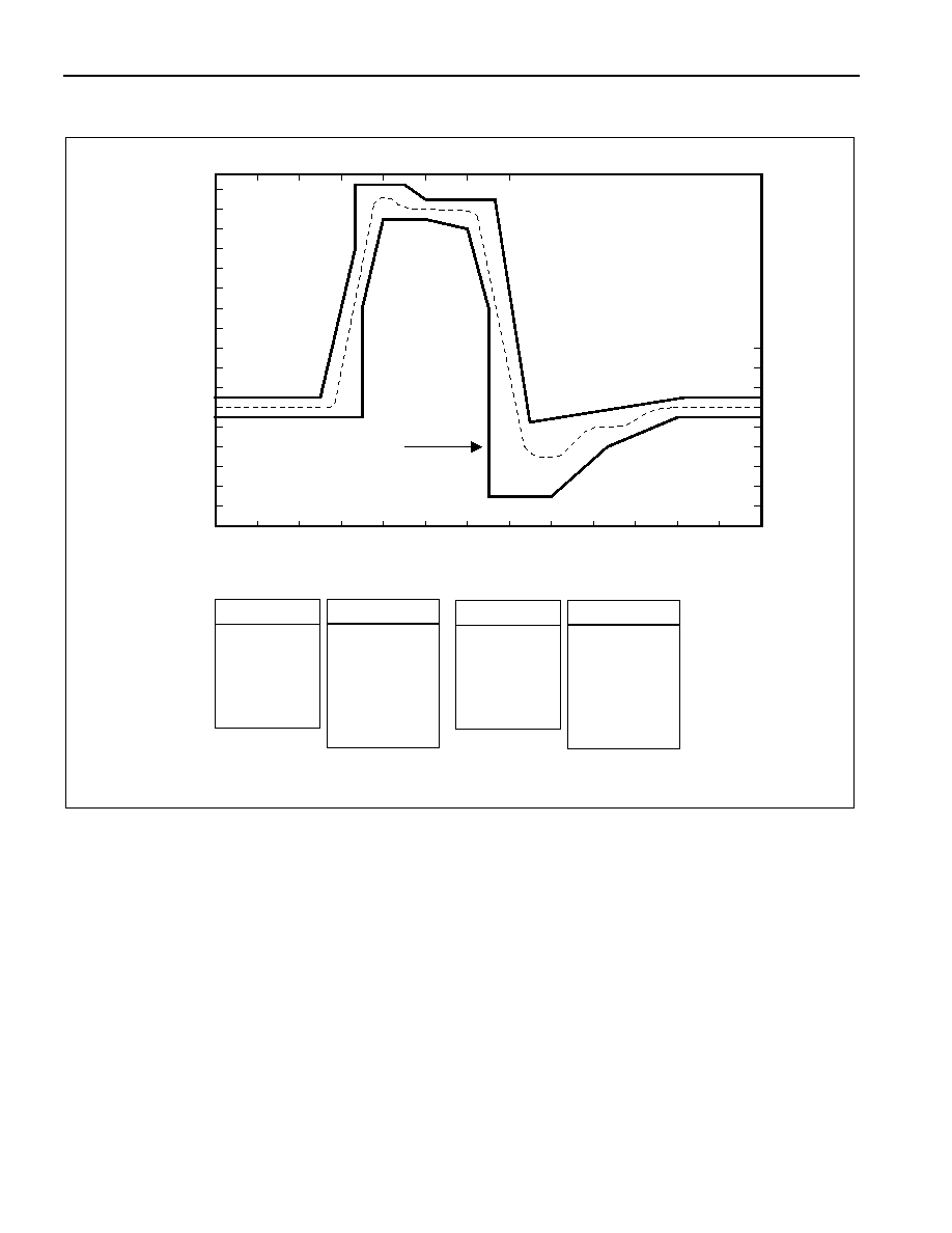
Dt
Dt
Dt

DS26324 3.3V, 16-Channel, E1/T1/J1, Short-Haul Line Interface Unit
27 of 112
Table 5-5. LIU Front-End Values
MODE COMPONENT
75
W COAX, 120W TWISTED PAIR, 100/110W TWISTED PAIR
Tx Capacitance
Ct
560pF typical. Adjust for board parasitics for optimal return
loss.
Tx Protection
Dt
1
International Rectifier 11DQ04 or 10BQ060
Motorola MBR0540T1
Rx Transformer RTR 1:1
TFr
Pulse TX1475
Tx Transformer 1:2
TFt
Halo TG83-S005NU
Rx Transformer RTR 1:2
TFr
Pulse T1124 (0∞C to +70∞C)
Tx Transformer 1:2
TFt
Pulse T1114 (-40∞C to +85∞C)
Tx Decoupling (TVDDn)
C1
Common decoupling for all 16 channels = 68
mF.
Tx Decoupling (TVDDn)
C2
Recommended decoupling per channel = 0.1
mF.
Rx Decoupling (AVDD)
C3
Common decoupling for all 16 channels = 68
mF.
Rx Decoupling (AVDD)
C4
Decouple all six pins separately with a 0.1
mF capacitor.
Rx Termination
C5
1
Rx capacitance for all 16 channels = 0.1
mF.
Rx Termination RTR 1:1
Rt
1
Needed two resistors for all modes = 60.4
W ±1%.
Rx Termination RTR 1:2
Rt
1
Needed two resistors for all modes = 15.0
W ±1%.
Voltage Protection
TVS1
SGS-Thomson SMLVT 3V3 (3.3V Transient Suppressor)
1
Only use if necessary for application.
5.4.3 Dual
Rail
Dual-rail mode consists of TPOS, TNEG and TCLK pins on the System side. NRZ data is sampled on the falling
edge of TCLK as shown in
Figure 9-12
. The Zero substitution B8ZS or HDB3 is not allowed. The data that appears
on the TPOS pin will be output on TTIP and data on the TNEG will be output on TRING after pulse shaping. Single-
Rail Select Register (
SRMS)
is used for selection of dual-rail or single-rail mode. The data that arrives at the TPOS
and TNEG can be overwritten in the maintenance mode by setting the BERT Control Register (
BTCR
).
5.4.4 Single-Rail
Mode
Single-rail mode consists of TPOS, TNEG and TCLK pins on the system side. NRZ data is sampled on the falling
edge of TCLK as shown in
Figure 9-12
. The Zero substitution B8ZS or HDB3 is allowed. The TPOS data will be
encoded in AMI or B8ZS/HDB3 format on the TTIP and TRING pins after pulse shaping. Single-Rail Mode Select
(
SRMS)
is used for selection of dual-rail or single-rail mode. The data that arrives at the TPOS can be overwritten
in the maintenance mode by setting in BERT Control Register (
BTCR
).
5.4.5 Zero Suppression--B8ZS or HDB3
B8ZS coding is available when the device is in T1 mode (selected by TS2, TS1 and TS0 bits in the
TS
register.
B8ZS/HDB3 coding are enabled by default in single-rail mode. Setting the LCS bit in the
LCS
Register disables
B8ZS/HDB3. Note that if the individual LIU is configured in E1 mode then HDB3 code substitution will be selected.
Bipolar violations can be inserted via the BEIR register or Transmit Maintenance Register settings only if B8ZS or
HDB3 coding is turned off.
B8ZS substitution is defined in ANSI T1.102 and HDB3 in ITUT G.703 standards.
5.4.6 Transmit
Power-Down
The Transmitter will be powered down if the relevant bits in the
TPDE
are set. The TTIP/TRING outputs will be
High-Z when TPDE is set.

DS26324 3.3V, 16-Channel, E1/T1/J1, Short-Haul Line Interface Unit
28 of 112
5.4.7 Transmit
All
Ones
When Transmit All Ones is invoked continuous Ones are transmitted using MCLK as the Timing Reference. Data
input at TPOS and TNEG is ignored.
Transmit All ones can be sent by setting bits in the
TAOE
Register. Also Transmit All ones will be enabled if bits in
Register
ATAOS
are set and the corresponding receiver goes into LOS state in status register
LOSS.
5.4.8 Drive
Failure
Monitor
The Driver Fail Monitor is connected to the TTIP and TRING pins. It will detect a Short or Open Circuit on the
Secondary side of the Transmit Transformer. The drive current will be limited to 50 ma if a short circuit is detected.
The
DFMS
status registers and the corresponding Interrupt and Enable Registers can be used to monitor the driver
failure.
5.5
Receiver
The 16 receivers of DS26324 are all identical. Either a 2:1 or 1:1 transformer can be used on the receive side
(selected by the RTR bit). The DS26324 is designed to be fully software-selectable for E1 and T1/J1 without the
need to change any external resistors for the receive-side. The receive impedance match settings are controlled by
the transmit template/impedance selection. See
Figure 5-8
and
Table 5-5
for external component values. Internal
impedance matching is enabled via the RIMPON bit.
The peak detector and data slicer process the received signal. The output of the data slicer goes to clock and data
recovery. A 2.048/1.544 PLL is internally multiplied by 16 via another internal PLL and fed to the clock recovery
system derives E1 or T1 clock. The clock recovery system uses the clock from the PLL circuit to form a 16 times
over sampler, which is used to recover the clock and data. This over sampling technique offers outstanding
performance to meet jitter tolerance specifications. Dependent on selection options B8ZS/HDB3/AMI decoding is
performed. These decoded data is provided to the system side in either single-rail or dual-rail mode. The selection
of single rail or dual rail is done by settings in the
SRMS
register.
The receiver is capable of recovering signals up to 18dB worth of attenuation. The receiver contains functionality to
provide resistive gain up to 20dB for monitor mode.
5.5.1 Receiver Monitor Mode
The receive equalizer is equipped with a monitor mode function that allows for resistive gain up to 20dB along with
cable attenuation of 6dB to 24dB as shown in the
RSMM1≠4
register.
5.5.2 Peak Detector and Slicer
The Slicer determines the polarity and presence of the received data. The output of the Slicer is sent to the Clock
and Data Recovery circuitry for extraction of data and clock. The slicer has a built-in peak detector for
determination of the slicing threshold.
5.5.3 Receive Level Indicator
The DS26324 will report the signal strength at RTIP and RRING in increments described in
Table 6-18
via register
bits CnRL3-CnRL0 located in the
RSL1≠4
register.

DS26324 3.3V, 16-Channel, E1/T1/J1, Short-Haul Line Interface Unit
29 of 112
5.5.4 Clock and Data Recovery
The resultant E1 or T1 clock derived from the 2.048/1.544 PLL is internally multiplied by 16 via another internal PLL
and fed to the clock recovery system. The clock recovery system uses the clock from the PLL circuit to form a 16
times over sampler, which is used to recover the clock and data. This over sampling technique offers outstanding
performance to meet jitter tolerance specifications.
5.5.5 Loss of Signal
The DS26324 uses both the Digital and Analog loss detection method in compliance with the latest T1.231 for
T1/J1 and ITU G.775 or ETSI 300 233 for E1 mode of operation.
LOS is detected if the receiver level falls bellow a threshold analog voltage for a certain duration. Alternatively this
can be termed as having received "zeros" for certain duration. The signal level and timing duration are defined in
accordance with the T1.231 or G.775 or ETSI 300 233 specifications.
The Loss Detection Thresholds are based on cable loss of 18dB for both T1 and E1 modes.
RCLK is replaced by MCLK when the receiver detects a Loss of signal. If the AISEL bit is set in the
GC
register or
the
IAISEL
bit is set, the RPOS/RNEG data is replaced by AIS. The loss state is exited when the receiver detects a
certain number of ones density at a higher signal level than the loss detection level. The loss detection signal level
and loss reset signal level are defined with a hysteresis to prevent the receiver from bouncing between "LOS" and
"no LOS" states.
The following Table outlines the specifications governing the loss function:
Table 5-6. Loss Criteria T1.231, G.775, and ETSI 300 233 Specifications
STANDARD
CRITERIA
T1.231
ITU G.775
ETSI 300 233
Loss
Detection
Criteria
No pulses are detected for 175
±75 bits.
No pulses are detected for
duration of 10 to 255 bit
periods.
No pulses are detected for a
duration of 2048 bit periods or
1ms.
Loss Reset
Criteria
Loss is terminated if a duration
of 12.5% ones are detected
over duration of 175 ±75 bits.
Loss is not terminated if 8
consecutive zeros are found if
B8ZS encoding is used. If
B8ZS is not used loss is not
terminated if 100 consecutive
pulses are zero.
The incoming signal has
transitions for duration of 10 to
255 bit periods.
Loss reset criteria is not
defined.
5.5.5.1 4.5.3.1 ANSI T1.231 for T1 and J1 Modes
Loss is detected if the received signal level is less than 200mV for duration of 192 bit periods. LOS is reset if the all
of the following criteria are met:
∑ 24 or more ones are detected in 192-bit period with a detection threshold of 300mV measured at
RTIP and RRING.
∑ During the 192 bits less than 100 consecutive zeros are detected.
∑ 8 consecutive zeros are not detected if B8ZS is set.
5.5.5.2 4.5.3.1 ITU G.775 for E1 Modes
LOS is detected if the received signal level is less than 200mV for a continuous duration of 192 bit periods. LOS is
reset if the receive signal level is greater than 300mV for a duration of 192 bit periods.
5.5.5.3 4.5.3.1 ETSI 200 233 for E1 Modes
LOS is detected if the received signal level is less than 200mV for a continuous duration of 2048 (1ms) bit periods.
LOS is reset if the receive signal level is greater than 300mV for a duration of 192 bit periods.

DS26324 3.3V, 16-Channel, E1/T1/J1, Short-Haul Line Interface Unit
30 of 112
5.5.6 AIS
Table 5-7
outlines the DS26324 AIS related specifications.
Table 5-8
states the AIS functionality in the DS26324.
The registers related to the AIS detection are shown in
Table 5-9
.
Table 5-7. AIS Criteria T1.231, G.775, and ETSI 300 233 Specifications
STANDARD
CRITERIA
ITU G.775 for E1
ETSI 300233 for E1
ANSI T1.231 for T1
AIS
Detection
Criteria
2 or fewer zeros in each of 2
consecutive 512-bit streams
received.
Less than 3 zeros detected in
512-bit period.
Fewer than 9 zeros detected in
a 8192-bit period (a ones
density of 99.9% over a period
of 5.3ms) are received.
AIS
Clearance
Criteria
3 or more zeros in each of 2
consecutive 512-bit streams
received.
3 or more zeros in a 512 bits
received.
9 or more zeros detected in a
8192-bit period are received.
Table 5-8. AIS Detection and Reset Criteria
STANDARD
CRITERIA
ITU G.775 for E1
ETSI 300233 for E1
ANSI T1.231 for T1
AIS
Detection
Criteria
2 or less zeros in each of 2
consecutive 512-bit streams
received.
Less than 3 zeros detected in
512-bit period.
Fewer than 9 zeros contained
in 8192 bits.
AIS
Clearance
Criteria
3 or more zeros in each of 2
consecutive 512-bit streams
received.
3 or more zeros in 512 bits
received.
9 or more bits received in a
8192-bit stream.
Table 5-9. Registers Related to AIS Detection
REGISTER ACRONYM
POINTER
FUNCTIONALITY
LOS/AIS Criteria
LASCS
Section criteria for AIS (T1.231, G.775, ETSI 300233 for E1)
AIS Register
AIS
Set when AIS is detected.
AIS Enable Register
AISIE
If reset interrupt due to AIS is not generated.
AIS Interrupt
AISI
Latched if there is a change in AIS and the interrupt is
enabled.
DS26324 3.3V, 16-Channel, E1/T1/J1, Short-Haul Line Interface Unit
31 of 112
5.5.7 Bipolar Violation and Excessive Zero detector
DS26324 detects code violations, BPV and excessive zero errors. The reporting of the errors is done through the
pin RNEGn/CVn.
Excessive zeros are detected if 8 consecutive zeros are detected with B8ZS enabled and 4 consecutive zeros are
detected with HDB3 enabled. Excessive Zero detection is selectable when single-rail mode and HDB3/B8ZS
encoding/decoding is selected.
The bits in
EZDE
and
CVDEB
registers determine the combinations that are reported.
Table 5-10
outlines the
functionality:
Table 5-10. BPV, Code Violation, and Excessive Zero Error Reporting
CONDITIONS
CVn PIN REPORTS
EZDE is reset, CVDEB is reset
BPV + Code violation
EZDE is set, CVDEB is reset
BPV + Code violation + Excessive zero
EZDE is reset, CVDEB is set
BPV
EZDE is set, CVDEB is set
BPV + Excessive zero
5.6 Jitter
Attenuator
The DS26324 contains an onboard jitter attenuator that can be set to a depth of either 32 or 128 bits via the JADS
bit in register
GC.
It can also be controlled on an individual LIU basis by settings in the
IJAFDS
register.
The 128-bit mode is used in applications where large excursions of wander are expected. The 32-bit mode is used
in delay sensitive applications. The characteristics of the attenuation are shown in
Figure 5-9
. The jitter attenuator
can be placed in either the receive path or the transmit path or none by appropriately setting the JAPS and the JAE
bits in register
GC
. These selections can be changed on an individual LIU basis by settings in the
IJAPS
and
IJAE
.
In order for the jitter attenuator to operate properly, a 2.048MHz or multiple thereof or 1.544MHz clock or multiple
thereof must be applied at MCLK. ITU specification G.703 requires an accuracy of ±50ppm for both T1 and E1
Applications. TR62411 and ANSI specs require an accuracy of ±32ppm for T1 interfaces. On-board circuitry
adjusts either the recovered clock from the clock/data recovery block or the clock applied at the TCLK pin to create
a smooth jitter-free clock, which is used to clock data out of the jitter attenuator FIFO. It is acceptable to provide a
jittery clock at the TCLK pin if the jitter attenuator is placed on the transmit side. If the incoming jitter exceeds either
120UI
P-P
(buffer depth is 128 bits) or 28UI
P-P
(buffer depth is 32 bits), then the DS26324 will divide the internal
nominal 32.768MHz (E1) or 24.704MHz (T1) clock by either 15 or 17 instead of the normal 16 to keep the buffer
from overflowing. When the device divides by either 15 or 17, it also sets the Jitter Attenuator Limit Trip (JALT) bits
in the
IJAFLT
register described.

DS26324 3.3V, 16-Channel, E1/T1/J1, Short-Haul Line Interface Unit
32 of 112
Figure 5-9. Jitter Attenuation
FREQUENCY (Hz)
0dB
-20dB
-40dB
-60dB
1
10
100
1K
10K
JITTER
ATT
E
NUAT
I
ON (dB)
100K
TR 62411 (Dec. 90)
Prohibited Area
C
urv
e B
Cu
rve
A
ITU G.7XX
Prohibited Area
TBR12
Prohibited
Area
T1
E1
5.7 G.772
Monitor
In this application, only 14 transceivers are functional and two transceivers are used for nonintrusive monitoring of
input and output of the other 14 channels. Channel 9 is used for channels 10 to 16 and Channel 1 is used for
channels 2 to 8. G.772 monitoring is configured by
GMC
registers (see
Table 6-9
). While monitoring channel 1 can
be configured in remote loopback and the monitored signal can be output on TTIP1 and TRING1. While monitoring
channel 9 can be configured in remote loopback and the monitored signal can be output on TTIP9 and TRING9.
5.8 Loopbacks
The DS26324 provides 4 loopbacks for diagnostic purposes: analog loopback, digital loopback, remote loopback,
and dual loopback. Dual loopback is accomplished by turning on digital loopback and remote loopback at the same
time.
5.8.1 Analog
Loopback
The analog output of the transmitter TTIP and TRING is looped back to RTIP and RRING of the receiver. Data at
RTIP and ring is ignored in analog loopback. This is shown in
Figure 5-10
.

DS26324 3.3V, 16-Channel, E1/T1/J1, Short-Haul Line Interface Unit
33 of 112
Figure 5-10. Analog Loopback
Line
Driver
H D B 3 /
B 8 Z S
E n c o d e r
O p t i o n a l
J i t t e r
A t t e n u a t o r
T r a n s m i t
D i g i t a l
T r a n s m i t
A n a l o g
TCLK
TPOS
TNEG
H D B 3 /
B 8 Z S
D e c o d e r
O p t i o n a l
J i t t e r
A t t e n u a t o r
R e c e i v e
D i g i t a l
R e c e i v e
A n a l o g
RCLK
RPOS
RNEG
Rtip
Rring
5.8.2 Digital
Loopback
The transmit system data TPOS and TNEG and TCLK will be looped back to output on RCLK, RPOS and RNEG.
The data input at TPOS and TNEG will be encoded and output on TTIP and TRING. Signals at RTIP and RRING
will be ignored. This loopback is conceptually shown in
Figure 5-11
.
Figure 5-11. Digital Loopback
Line
Driver
H D B 3 /
B 8 Z S
E n c o d e r
O p t i o n a l
J i t t e r
A t t e n u a t o r
T r a n s m i t
D i g i t a l
T r a n s m i t
A n a l o g
TCLK
TPOS
TNEG
H D B 3 /
B 8 Z S
D e c o d e r
O p t i o n a l
J i t t e r
A t t e n u a t o r
R e c e i v e
D i g i t a l
R e c e i v e
A n a l o g
RCLK
RPOS
RNEG
RTIP
RRING
TPOS
TNEG
TTIP
TRING

DS26324 3.3V, 16-Channel, E1/T1/J1, Short-Haul Line Interface Unit
34 of 112
5.8.3 Remote
Loopback
The inputs at RTIP and RRING are looped back to TTIP and TRING. The inputs at TCLK, TPOS and TNEG are
ignored during a remote loopback. This loopback is conceptually shown in
Figure 5-12
.
Note: Remote loopback does not take precedence over Transmit Power-Down and requires TCLK to operate. The
transmitters will use the recovered RCLK in remote loopback. TCLK is still required because if it is removed the
transmitters will power-down (TCLK held low) or transmit all ones (TCLK held high).
Figure 5-12. Remote Loopback
Line
Driver
H D B 3 /
B 8 Z S
E n c o d e r
O p t i o n a l
J i t t e r
A t t e n u a t o r
T r a n s m i t
D i g i t a l
T r a n s m i t
A n a l o g
TCLK
TPOS
TNEG
H D B 3 /
B 8 Z S
D e c o d e r
O p t i o n a l
J i t t e r
A t t e n u a t o r
R e c e i v e
D i g i t a l
R e c e i v e
A n a l o g
RCLK
RPOS
RNEG
RTIP
RRING
TPOS
TNEG
5.9 BERT
There are two bit error rate testers available on the DS26324. One BERT can be mapped into LIUs 1-8 and the
other into LIUs 9-16 via the
BTCR
registers. The two BERTs operate independently of each other.
5.9.1 General
Description
The BERT is a software programmable test pattern generator and monitor capable of meeting most error
performance requirements for digital transmission equipment. It will generate and synchronize to pseudorandom
patterns with a generation polynomial of the form x
n
+ x
y
+ 1, where n and y can take on values from 1 to 32 and to
repetitive patterns of any length up to 32 bits.
The transmit direction generates the programmable test pattern, and inserts the test pattern payload into the data
stream.
The receive direction extracts the test pattern payload from the receive data stream, and monitors the test pattern
payload for the programmable test pattern.
Features
∑ Programmable PRBS pattern ≠ The Pseudo Random Bit Sequence (PRBS) polynomial (x
n
+ x
y
+ 1) and seed
are programmable (length n = 1 to 32, tap y = 1 to n ≠ 1, and seed = 0 to 2
n
≠ 1).
∑ Programmable repetitive pattern ≠ The repetitive pattern length and pattern are programmable (the length n
= 1 to 32 and pattern = 0 to 2
n
≠ 1).
∑ 24-bit error count and 32-bit bit count registers
∑ Programmable bit error insertion ≠ Errors can be inserted individually, on a pin transition, or at a specific
rate. The rate 1/10
n
is programmable (n = 1 to 7).
∑ Pattern synchronization at a 10
-3
BER ≠ Pattern synchronization will be achieved even in the presence of a
random Bit Error Rate (BER) of 10
-3
.
TTIP
TRING

DS26324 3.3V, 16-Channel, E1/T1/J1, Short-Haul Line Interface Unit
35 of 112
5.9.2 Configuration
and
Monitoring
Set BTCR.BERTE = 1 to enable the BERT. The following tables show how to configure the on-board BERT to send
and receive common patterns.
Table 5-11. Pseudorandom Pattern Generation
BPCR REGISTER
BERT.CR
PATTERN TYPE
PTF[4:0]
(hex)
PLF[4:0]
(hex)
PTS QRSS
BERT.
PCR
BERT.
SPR2
BERT.
SPR1
TPIC,
RPIC
2
9
-1
O.153 (511 type)
04
08
0
0
0x0408
0xFFFF 0xFFFF
0
2
11
-1
O.152 and O.153
(2047 type)
08 0A
0
0
0x080A
0xFFFF
0xFFFF
0
2
15
-1
O.151 0D
0E
0
0
0x0D0E
0xFFFF
0xFFFF
1
2
20
-1
O.153 10
13
0
0
0x1013
0xFFFF
0xFFFF
0
2
20
-1
O.151 QRSS
02
13
0
1
0x0253
0xFFFF 0xFFFF
0
2
23
-1
O.151 11
16
0
0
0x1116
0xFFFF
0xFFFF
1
Table 5-12. Repetitive Pattern Generation
BPCR REGISTER
PATTERN TYPE
PTF[4:0]
(hex)
PLF[4:0]
(hex)
PTS QRSS
BERT.
PCR
BERT.
SPR2
BERT.
SPR1
All ones
NA
00
1
0
0x0020
0xFFFF
0xFFFF
All zeros
NA
00
1
0
0x0020
0xFFFF
0xFFFE
Alternating ones and zeros
NA
01
1
0
0x0021
0xFFFF
0xFFFE
Double alternating and zeros NA 03
1
0 0x0023
0xFFFF
0xFFFC
3 in 24
NA
17
1
0
0x0037
0xFF20
0x0022
1 in 16
NA
0F
1
0 0x002F
0xFFFF
0x0001
1 in 8
NA
07
1
0 0x0027
0xFFFF
0xFF01
1 in 4
NA
03
1
0
0x0023
0xFFFF
0xFFF1
After configuring these bits, the pattern must be loaded into the BERT. This is accomplished via a zero-to-one
transition on
BCR
.TNPL and
BCR
.RNPL
Monitoring the BERT requires reading the
BSR
Register, which contains the Bit Error Count (BEC) bit and the Out
of Synchronization (OOS) bit.
The BEC bit will be one when the bit error counter is one or more.
The OOS will be
one when the receive pattern generator is not synchronized to the incoming pattern, which will occur when it
receives a minimum 6 bit errors within a 64 bit window.
The Receive BERT Bit Count Register (
RBCR
) and the
Receive BERT Bit Error Count Register (
RBECR
) will be updated upon the reception of a Performance Monitor
Update signal (e.g.
BCR.
LPMU).
This signal will update the registers with the values of the counters since the last
update and will reset the counters.

DS26324 3.3V, 16-Channel, E1/T1/J1, Short-Haul Line Interface Unit
36 of 112
5.9.3 Receive Pattern Detection
The Receive BERT receives only the payload data and synchronizes the receive pattern generator to the incoming
pattern. The receive pattern generator is a 32-bit shift register that shifts data from the least significant bit (LSB) or
bit 1 to the most significant bit (MSB) or bit 32. The input to bit 1 is the feedback. For a PRBS pattern (generating
polynomial x
n
+ x
y
+ 1), the feedback is an XOR of bit n and bit y. For a repetitive pattern (length n), the feedback is
bit n. The values for n and y are individually programmable (1 to 32). The output of the receive pattern generator is
the feedback. If QRSS is enabled, the feedback is an XOR of bits 17 and 20, and the output will be forced to one if
the next 14 bits are all zeros. QRSS is programmable (on or off). For PRBS and QRSS patterns, the feedback will
be forced to one if bits 1 through 31 are all zeros. Depending on the type of pattern programmed, pattern detection
performs either PRBS synchronization or repetitive pattern synchronization.
5.9.3.1 Receive PRBS Synchronization
PRBS synchronization synchronizes the receive pattern generator to the incoming PRBS or QRSS pattern. The
receive pattern generator is synchronized by loading 32 data stream bits into the receive pattern generator, and
then checking the next 32 data stream bits. Synchronization is achieved if all 32 bits match the incoming pattern. If
at least six incoming bits in the current 64-bit window do not match the receive pattern generator, automatic pattern
re-synchronization is initiated. Automatic pattern re-synchronization can be disabled.
See
Figure 5-13
for the PRBS synchronization diagram.
Figure 5-13. PRBS Synchronization State Diagram
Sync
Load
Verify
1 bit error
32 bits loaded
32
b
its
w
ith
ou
t e
rr
or
s
6 o
f 6
4 b
its
w
ith
er
ro
rs

DS26324 3.3V, 16-Channel, E1/T1/J1, Short-Haul Line Interface Unit
37 of 112
5.9.3.2 Receive Repetitive Pattern Synchronization
Repetitive pattern synchronization synchronizes the receive pattern generator to the incoming repetitive pattern.
The receive pattern generator is synchronized by searching each incoming data stream bit position for the
repetitive pattern, and then checking the next 32 data stream bits. Synchronization is achieved if all 32 bits match
the incoming pattern. If at least six incoming bits in the current 64-bit window do not match the receive PRBS
pattern generator, automatic pattern re-synchronization is initiated. Automatic pattern re-synchronization can be
disabled.
Figure 5-14 shows the repetitive pattern synchronization state diagram.
Figure 5-14. Repetitive Pattern Synchronization State Diagram
Sync
Match
Verify
1 bit error
Pattern Matches
32
b
its
w
ith
ou
t e
rr
or
s
6 o
f 6
4 b
its
w
ith
er
ro
rs
5.9.3.3 Receive Pattern Monitoring
Receive pattern monitoring monitors the incoming data stream for both an OOS condition and bit errors and counts
the incoming bits. An Out Of Synchronization (OOS) condition is declared when the synchronization state machine
is not in the "Sync" state. An OOS condition is terminated when the synchronization state machine is in the "Sync"
state.
Bit errors are determined by comparing the incoming data stream bit to the receive pattern generator output. If they
do not match, a bit error is declared, and the bit error and bit counts are incremented. If they match, only the bit
count is incremented. The bit count and bit error count are not incremented when an OOS condition exists.

DS26324 3.3V, 16-Channel, E1/T1/J1, Short-Haul Line Interface Unit
38 of 112
5.9.4 Transmit Pattern Generation
Pattern Generation generates the outgoing test pattern, and passes it onto Error Insertion. The transmit pattern
generator is a 32-bit shift register that shifts data from the least significant bit (LSB) or bit 1 to the most significant
bit (MSB) or bit 32. The input to bit 1 is the feedback. For a PRBS pattern (generating polynomial x
n
+ x
y
+ 1), the
feedback is an XOR of bit n and bit y. For a repetitive pattern (length n), the feedback is bit n. The values for n and
y are individually programmable (1 to 32). The output of the receive pattern generator is the feedback. If QRSS is
enabled, the feedback is an XOR of bits 17 and 20, and the output will be forced to one if the next 14 bits are all
zeros. QRSS is programmable (on or off). For PRBS and QRSS patterns, the feedback will be forced to one if bits
1 through 31 are all zeros. When a new pattern is loaded, the pattern generator is loaded with a seed/pattern value
before pattern generation starts. The seed/pattern value is programmable (0 ≠ 2
n
≠ 1).
5.9.4.1 Transmit Error Insertion
Error insertion inserts errors into the outgoing pattern data stream. Errors are inserted one at a time or at a rate of
one out of every 10
n
bits. The value of n is programmable (1 to 7 or off). Single bit error insertion can be initiated
from the microprocessor interface, or by the manual error insertion input (TMEI). The method of single error
insertion is programmable (register or input). If pattern inversion is enabled, the data stream is inverted before the
overhead/stuff bits are inserted. Pattern inversion is programmable (on or off).

DS26324 3.3V, 16-Channel, E1/T1/J1, Short-Haul Line Interface Unit
39 of 112
6 REGISTER MAPS AND DEFINITION
Six address bits are used to control the settings of the registers. In the parallel nonmultiplexed mode address [5:0]
is used. In multiplexed mode AD [5:0] is used and A [6:1] is used in the serial mode. The register space contains
two independent sets of registers. The lower set of registers is located from address 00 hex to 1F hex and contains
controls for LIUs 1-8. The upper set of registers is a duplicate of the lower set, located from address 20 hex to 3F
hex, which controls LIUs 9-16. Each of these sets of registers consists of 4 banks (Primary, Secondary, Individual
LIU, and BERT). The
ADDP
register for the lower set of registers is located at address 1F hex. This register is used
as a pointer to access the 4 banks of registers in the lower (LIUs 1-8) register set. Similarly, the
ADDP
register for
the upper set of registers is located at address 3F hex. This register is used as a pointer to access the 4 banks of
registers in the upper (LIUs 9-16) register set. Setting an ADDP register to AA hex will access the Secondary bank
of registers, 01 hex will access the Individual LIU bank of registers, 02 hex will access the BERT bank of registers,
and 00 hex (default on power-up) will access the Primary bank of registers. Note that bank selection for the lower
set of registers is controlled only by the ADDP at 1F hex and that bank selection for the upper set of registers is
controlled only by the ADDP at 3F hex.

DS26324 3.3V, 16-Channel, E1/T1/J1, Short-Haul Line Interface Unit
40 of 112
Table 6-1. Primary Register Set
ADDRESS FOR CH 1≠8
ADDRESS FOR CH 9≠16
NAME SYMBOL
HEX
FOR CH
1≠8
PARALLEL
INTERFACE
A7≠A0
(HEX)
SERIAL
INTERFACE
A7≠A1
(HEX)
HEX FOR
CH 9≠16
PARALLEL
INTERFACE
A7≠A0
(HEX)
SERIAL
INTERFACE
A7-A1
(HEX)
RW
Identification
ID
00
xx000000
x000000
20
Not used
Not used
R
Analog Loopback Configuration
ALBC
01
xx000001
x000001
21
xx100001
x100001
RW
Remote Loopback Configuration
RLBC
02
xx000010
x000010
22
xx100010
x100010
RW
Transmit All Ones Enable
TAOE
03
xx000011
x000011
23
xx100011
x100011
RW
LOS Status
LOSS
04
xx000100
x000100
24
xx100100
x100100
R
Driver Fault Monitor Status
DFMS
05
xx000101
x000101
25
xx100101
x100101
R
LOS
Interrupt
Enable
LOSIE 06 xx000110 x000110 26 xx100110
x100110
RW
Driver Fault Monitor Interrupt Enable
DFMIE
07
xx000111
x000111
27
xx100111
x100111
RW
LOS Interrupt Status
LOSIS
08
xx001000
x001000
28
xx101000
x101000
R
Driver Fault Monitor Interrupt
Status
DFMIS 09 xx001001 x001001 29 xx101001
x101001 R
Software Reset
SWR
0A
xx001010
x001010
2A
xx101010
x101010
W
G.772
Monitor
Configuration
GMC 0B xx001011 x001011 2B xx101011
x101011
RW
Digital Loopback Configuration
DLBC
0C
xx001100
x001100
2C
xx101100
x101100
RW
LOS/AIS Criteria Selection
LASCS
0D
xx001101
x001101
2D
xx101101
x101101
RW
Automatic Transmit All Ones
Select
ATAOS 0E xx001110 x001110 2E xx101110
x101110
RW
Global
Configuration
GC 0F xx001111 x001111 2F xx101111
x101111
RW
Template Select Transceiver
Register
TST 10 xx010000
x010000 30 xx110000
x110000
RW
Template Select
TS
11
xx010001
x010001
31
xx110001
x110001
RW
Output Enable
OE
12
xx010010
x010010
32
xx110010
x110010
RW
Alarm Indication Signal
AIS
13
xx010011
x010011
33
xx110011
x110011
R
AIS Interrupt Enable
AISIE
14
xx010100
x010100
34
xx110100
x110100
RW
AIS Interrupt Status
AISIS
15
xx010101
x010101
35
xx110101
x110101
R
Reserved --
16≠1E
xx010110≠
xx011110
x010110≠
x011110
36≠3E
xx110110≠
x111110
x110110≠
x111110
--
Address Pointer for Bank Selection
ADDP
1F
xx011111
x011111
3F
xx111111
x111111
RW

DS26324 3.3V, 16-Channel, E1/T1/J1, Short-Haul Line Interface Unit
41 of 112
Table 6-2. Secondary Register Set
ADDRESS FOR
CHANNELS 1≠8
ADDRESS FOR
CHANNELS 9-16
NAME SYMBOL
HEX
FOR
CH 1≠8
PARALLEL
INTERFACE
A7≠A0
(HEX)
SERIAL
INTERFACE
A7≠A1
(HEX)
HEX
FOR
CH 9≠16
PARALLEL
INTERFACE
A7≠A0
(HEX)
SERIAL
INTERFACE
A7≠A1
(HEX)
RW
Single-Rail
Mode
Select
SRMS 00 xx000000 x000000 20 xx100000 x100000 RW
Line
Code
Selection
LCS
01 xx000001 x000001 21 xx100001 x100001 R
Not
Used
--
02 xx000010 x000010 22 xx100010 x100010 R
Receive Power-Down Enable
RPDE
03
xx000011
x000011
23
xx100011
x100011
RW
Transmit
Power-Down
Enable TPDE 04 xx000100 x000100 24 xx100100 x100100 RW
Excessive Zero Detect Enable
EZDE
05
xx000101
x000101
25
xx100101
x100101
R
Code Violation Detect Enable
Bar
CVDEB 06 xx000110 x000110 26 xx100110 x100110 R
Not Used
--
07≠1E
xx000111≠
xx011110
x000111≠
x011110
27≠3E
xx100111≠
xx111110
x100111≠
x111110
W
Address Pointer for Bank
Selection
ADDP 1F xx011111 x011111 3F xx111111 x111111 RW

DS26324 3.3V, 16-Channel, E1/T1/J1, Short-Haul Line Interface Unit
42 of 112
Table 6-3. Individual LIU Register Set
ADDRESS FOR
CHANNELS 1≠8
ADDRESS FOR
CHANNELS 9≠16
NAME SYMBOL
HEX
FOR
CH 1≠8
PARALLEL
INTERFACE
A7≠A0
(HEX)
SERIAL
INTERFACE
A7≠A1
(HEX)
HEX
FOR
CH 9≠16
PARALLEL
INTERFACE
A7≠A0
(HEX)
SERIAL
INTERFACE
A7≠A1 (HEX)
RW
Individual JA Enable
IJAE
00
xx000000
x000000
20
xx100000
x100000
RW
Individual JA Position Select
IJAPS
01
xx000001
x000001
21
xx100001
x100001
RW
Individual JA FIFO Depth
Select
IJAFDS 02 xx000010 x000010 22 xx100010 x100010
RW
Individual JA FIFO Limit Trip
IJAFLT
03
xx000011
x000011
23
xx100011
x100011
R
Individual Short Circuit
Protection Disable
ISCPD 04 xx000100
x000100 24 xx100100 x100100
RW
Individual AIS Select
IAISEL
05
xx000101
x000101
25
xx100101
x100101
RW
Master Clock Select
MC
06
xx000110
x000110
26
Not used
Not used
RW
Receive Sensitivity Monitor
Mode 1≠4
RSMM1≠4 08≠0B
xx001000≠
xx001011
x001000≠
x001011
28≠2B
xx101000≠
xx101011
x101000≠
x101011
RW
Receive Signal Level
Indicator 1≠4
RSL1≠4 0C≠0F
xx001100≠
xx001111
x001100≠
x001111
2C≠2F
xx101100≠
xx101111
x101100≠
x101111
R
Bit Error Rate Tester Control
Register
BTCR 10 xx010000
x010000 30 xx110000
x110000
RW
Line Violation Detect Status
LVDS
12
xx010010
x010010
32
xx110010
x110010
R
Receive Clock Invert
RCLKI
13
xx010011
x010011
33
xx110011
x110011
RW
Transmit Clock Invert
TCLKI
14
xx010100
x010100
34
xx110100
x110100
RW
Clock Control Register
CCR
15
xx010101
x010101
35
Not used
Not used
RW
RCLK Disable Upon LOS
Register
RDULR 16 xx010110 x010110 36 xx110110 x110110
RW
Global Interrupt Status
Control
GISC
1E
xx011110
x011110
3E
Not used
Not used
RW
Address Pointer for Bank
Selection
ADDP 1F xx011111
x011111 3F xx111111 x111111
RW

DS26324 3.3V, 16-Channel, E1/T1/J1, Short-Haul Line Interface Unit
43 of 112
Table 6-4. BERT Register Set
ADDRESS FOR
CHANNELS 1≠8
ADDRESS FOR CHANNELS
9≠16
NAME SYMBOL
HEX
FOR
CH 1≠8
PARALLEL
INTERFACE
A7≠A0
(HEX)
SERIAL
INTERFACE
A7≠A1
(HEX)
HEX
FOR
CH 9≠16
PARALLEL
INTERFACE
A7≠A0
(HEX)
SERIAL
INTERFACE
A7≠A1
(HEX)
RW
BERT Control Register
BCR
00
xx000000
x000000
20
xx100000
x100000
RW
Reserved --
01
xx000001
x000001
21
xx100001
x100001
BERT Pattern Configuration 1
BPCR1
02
xx000010
x000010
22
xx100010
x100010
RW
BERT Pattern Configuration 2
BPCR2
03
xx000011
x000011
23
xx100011
x100011
RW
BERT Seed/Pattern 1
BSPR1
04
xx000100
x000100
24
xx100100
x100100
RW
BERT Seed/Pattern 2
BSPR2
05
xx000101
x000101
25
xx100101
x100101
RW
BERT Seed/Pattern 3
BSPR3
06
xx000110
x000110
26
xx100110
x100110
RW
BERT Seed/Pattern 4
BSPR4
07
xx000111
x000111
27
xx100111
x100111
RW
Transmit Error Insertion Control
TEICR
08
xx001000
x001000
28
xx101000
x101000
RW
Reserved --
09≠0A
xx001001≠
x001010
-- 29≠2A
xx101001≠
x101010
-- --
BERT Status Register
BSR
0C
xx001100
x001100
2C
xx101100
x101100
R
Reserved
0D
xx001101
x001101
2D
xx101101
x101101
BERT Status Register Latched
BSRL
0E
xx010011
x010011
2E
xx110011
x110011
RW
BERT Status Register Interrupt
Enable
BSRIE 10 xx010000 x010000 30 xx110000 x110000
RW
Reserved --
11≠13
xx010001≠
xx010011
x010001≠
x010011
31≠33
xx110001≠
xx110011
x110001≠
x110011
--
Receive Bit Error Count Register
1
RBECR1 14 xx010100 x010100 34
xx110100 x110100 R
Receive Bit Error Count Register
2
RBECR2 15 xx010101 x010101 35
xx110101 x110101 R
Receive Bit Error Count Register
3
RBECR3 16 xx010110 x010110 36
xx110110 x110110 R
Receive Bit Error Count Register
4
RBECR4 17 xx010111 x010111 37
xx110111 x110111 R
Receive Bit Count Register 1
RBCR1
18
xx011000
x011000
38
xx111000
x111000
R
Receive Bit Count Register 2
RBCR2
19
xx011001
x011001
39
xx111001
x111001
R
Receive Bit Count Register 3
RBCR3
1A
xx011010
x011010
3A
xx111010
x111010
R
Receive Bit Count Register 4
RBCR4
1B
xx011011
x011011
3B
xx111011
x111011
R
Reserved --
1C≠1E
xx011100≠
xx011110
x011100≠
x011110
3C≠3E
xx111100≠
xx111110
x111100≠
x111110
--
Address Pointer for Bank
Selection
ADDP 1F xx011111 x011111 3F xx111111 x111111
RW

DS26324 3.3V, 16-Channel, E1/T1/J1, Short-Haul Line Interface Unit
44 of 112
Table 6-5. Primary Register Set Bit Map
REGISTER
ADDRESS
FOR LIUS
1-8
R/W
BIT 7
BIT 6
BIT 5
BIT 4
BIT 3
BIT 2
BIT 1
BIT 0
ID 00
R
ID7 ID6 ID5 ID4 ID3 ID2 ID1 ID0
ALBC
01
RW ALC8 ALBC7 ALBC6 ALBC5 ALBC4 ALBC3 ALBC2 ALBC1
RLBC
02
RW RLBC8 RLBC7 RLBC6 RLBC5 RLBC4 RLBC3 RLBC2 RLBC1
TAOE
03
RW TAOE8 TAOE7 TAOE6 TAOE5 TAOE4 TAOE3 TAOE2 TAOE1
LOSS
04
RW LOSS8 LOSS7 LOSS6 LOSS5 LOSS4 LOSS3 LOSS2 LOSS1
DFMS 05
RW
DFMS8
DFMS7
DFMS6
DFMS5 DFMS4 DFMS3 DFMS2 DFMS1
LOSIE
06
RW LOSIE8 LOSIE7 LOSIE6 LOSIE5 LOSIE4 LOSIE3 LOSIE2 LOSIE1
DFMIE
07
RW DFMIE8 DFMIE7 DFMIE6 DFMIE5 DFMIE4 DFMIE3 DFMIE2 DFMIE1
LOSIS 08
R
LOSIS8 LOSIS7 LOSIS6 LOSIS5 LOSIS4 LOSIS3 LOSIS2 LOSIS1
DFMIS 09 R
DFMIS8 DFMIS7 DFMIS6 DFMIS5 DFMIS4 DFMIS3 DFMIS2 DFMIS1
SWR
0A
W SWRL SWRL SWRL SWRL SWRL SWRL SWRL SWRL
GMC 0B
RW
--
--
--
--
GMC4 GMC3 GMC2 GMC1
DLBC
0C
RW DLBC8 DLBC7 DLBC6 DLBC5 DLBC4 DLBC3 DLBC2 DLBC1
LASCS
0D
RW LASCS8 LASCS7 LASCS6 LASCS5 LASCS4 LASCS3 LASCS2 LASCS1
ATAOS
0E
RW ATAOS8 ATAOS7 ATAOS6 ATAOS5 ATAOS4 ATAOS3 ATAOS2 ATAOS1
GC 0F
RW
--
AISEL
SCPD
CODE
JADS
RTCTL
JAPS
JAE
TST 10
RW
--
--
--
--
--
TST2 TST1 TST0
TS 11
RW
RIMPON
TIMPOFF
--
--
TIMPRM TS2 TS1 TS0
OE
12 RW
OE8 OE7 OE6 OE5 OE4 OE3 OE2 OE1
AIS 13
R
AIS8 AIS7 AIS6 AIS5 AIS4 AIS3 AIS2 AIS1
AISIE
14
RW AISIE8 AISIE7 AISIE6 AISIE5 AISIE4 AISIE3 AISIE2 AISIE1
AISI 15
R
AISI8 AISI7 AISI6 AISI5 AISI4 AISI3 AISI2 AISI1
Not Used
16-1E
--
--
--
--
--
--
--
--
--
ADDP
1F
RW ADDP7 ADDP6 ADDP5 ADDP4 ADDP3 ADDP2 ADDP1 ADDP0
REGISTER
ADDRESS
FOR LIUs
9≠16
R/W
BIT 7
BIT 6
BIT 5
BIT 4
BIT 3
BIT 2
BIT 1
BIT 0
Not Used
20
R
--
--
--
--
--
--
--
--
ALBC
21
RW ALC16 ALBC15 ALBC14 ALBC13 ALBC12 ALBC11 ALBC10 ALBC9
RLBC
22
RW RLBC16 RLBC15 RLBC14 RLBC13 RLBC12 RLBC11 RLBC10 RLBC9
TAOE
23
RW TAOE16 TAOE15 TAOE14 TAOE13 TAOE12 TAOE11 TAOE10 TAOE9
LOSS
24
RW LOSS16 LOSS15 LOSS14 LOSS13 LOSS12 LOSS11 LOSS10 LOSS9
DFMS
25
RW DFMS16 DFMS15 DFMS14 DFMS13 DFMS12 DFMS11 DFMS10 DFMS9
LOSIE
26
RW LOSIE16 LOSIE15 LOSIE14 LOSIE13 LOSIE12 LOSIE11 LOSIE10 LOSIE9
DFMIE
27
RW DFMIE16 DFMIE15 DFMIE14 DFMIE13 DFMIE12 DFMIE11 DFMIE10 DFMIE9
LOSIS 28
R
LOSIS16 LOSIS15 LOSIS14 LOSIS13 LOSIS12 LOSIS11 LOSIS10 LOSIS9
DFMIS 29 R
DFMIS16 DFMIS15 DFMIS14 DFMIS13 DFMIS12 DFMIS11 DFMIS10 DFMIS9
SWR
2A
W SWRU SWRU SWRU SWRU SWRU SWRU SWRU SWRU
GMC 2B
RW
--
--
--
--
GMC4 GMC3 GMC2 GMC1
DLBC
2C
RW DLBC16 DLBC15 DLBC14 DLBC13 DLBC12 DLBC11 DLBC10 DLBC9
LASCS
2D
RW LASCS16 LASCS15 LASCS14 LASCS13 LASCS12 LASCS11 LASCS10 LASCS9
ATAOS 2E
RW
ATAOS16 ATAOS15 ATAOS14 ATAOS13 ATAOS12 ATAOS11 ATAOS10 ATAOS9
GC 2F
RW
--
AISEL
SCPD
CODE
JADS
--
JAPS
JAE
TST 30
RW
--
--
--
--
--
TST2 TST1 TST0
TS 31
RW
RIMPON
TIMPOFF
--
--
TIMPRM
TS2 TS1 TS0
OE
32 RW OE16 OE15 OE14 OE13 OE12 OE11 OE10 OE9
AIS 33
R
AIS16 AIS15 AIS14 AIS13 AIS12 AIS11 AIS10 AIS9
AISIE
34
RW AISIE16 AISIE15 AISIE14 AISIE13 AISIE12 AISIE11 AISIE10 AISIE9
AISI 35
R
AISI16 AISI15 AISI14 AISI13 AISI12 AISI11 AISI10 AISI9
Not Used
36-3E
--
--
--
--
--
--
--
--
--
ADDP
3F
RW ADDP7 ADDP6 ADDP5 ADDP4 ADDP3 ADDP2 ADDP1 ADDP0

DS26324 3.3V, 16-Channel, E1/T1/J1, Short-Haul Line Interface Unit
45 of 112
Table 6-6. Secondary Register Set Bit Map
REGISTER
ADDRESS
FOR LIUs
1≠8
RW
BIT 7
BIT 6
BIT 5
BIT 4
BIT 3
BIT 2
BIT 1
BIT 0
SRS
00
RW SRMS8 SRMS7 SRMS6 SRMS5 SRMS4 SRMS3 SRMS2 SRMS1
LCS
01 RW
LCS8 LCS7 LCS6 LCS5 LSC4 LCS3 LSC2 LSC1
Not Used
02
RW
--
--
--
--
--
--
--
--
RPDE
03
RW RPDE8 RPDE7 RPDE6 RPDE5 RPDE4 RPDE3 RPDE2 RPDE1
TPDE
04
RW TPDE8 TDPE7 TPDE6 TPDE5 TPDE4 TPDE3 TPDE2 TPDE1
EZDE
05
RW EZDE8 EZDE7 EZDE6 EZDE5 EZDE4 EZDE3 EZDE2 EZDE1
CVDEB
06
RW CVDEB8 CVDEB7 CVDEB6 CVDEB5 CVDEB4 CVDEB3 CVDEB2 CVDEB1
Not Used
07-1E
--
--
--
--
--
--
--
--
ADDP
1F
RW ADDP7 ADDP6 ADDP5 ADDP4 ADDP3 ADDP2 ADDP1 ADDP0
REGISTER
ADDRESS
FOR LIUs
9≠16
RW
BIT 7
BIT 6
BIT 5
BIT 4
BIT 3
BIT 2
BIT 1
BIT 0
SRS
20
RW SRMS16 SRMS15 SRMS14 SRMS13 SRMS12 SRMS11 SRMS10 SRMS9
LCS
21
RW LCS16 LCS15 LCS14 LCS13 LSC12 LCS11 LSC10 LSC9
Not Used
22
RW
--
--
--
--
--
--
--
--
RPDE
23
RW RPDE16 RPDE15 RPDE14 RPDE13 RPDE12 RPDE11 RPDE10 RPDE9
TPDE
24
RW TPDE16 TDPE15 TPDE14 TPDE13 TPDE12 TPDE11 TPDE10 TPDE9
EZDE
25
RW EZDE16 EZDE15 EZDE14 EZDE13 EZDE12 EZDE11 EZDE10 EZDE9
CVDEB 26
RW
CVDEB16 CVDEB15 CVDEB14 CVDEB13 CVDEB12 CVDEB11 CVDEB10 CVDEB9
Not
Used 27-3E -- --
--
--
--
--
--
--
--
ADDP
3F
RW ADDP7 ADDP6 ADDP5 ADDP4 ADDP3 ADDP2 ADDP1 ADDP0

DS26324 3.3V, 16-Channel, E1/T1/J1, Short-Haul Line Interface Unit
46 of 112
Table 6-7. Individual LIU Register Set Bit Map
REGISTER
ADDRESS
FOR LIUs
1≠8
RW
BIT 7
BIT 6
BIT 5
BIT 4
BIT 3
BIT 2
BIT 1
BIT 0
IJAE
00 RW IJAE8 IJAE7 IJAE6 IJAE5 IJAE4 IJAE3 IJAE2 IJAE1
IJAPS
01
RW IJAPS8 IJAPS7 IJAPS6 IJAPS5 IJAPS4 IJAPS3 IJAPS2 IJAPS1
IJAFDS
02
RW IJAFDS8 IJAFDS7 IJAFDS6 IJAFDS5 IJAFDS4 IJAFDS3 IJAFDS2 IJAFDS1
IJAFLT 03
R
IJAFLT8 IJAFLT7 IJAFLT6 IJAFLT5 IJAFLT4 IJAFLT3 IJAFLT2 IJAFLT1
ISCPD
04
RW ISCPD8 ISCPD7 ISCPD6 ISCPD5 ISCPD4 ISCPD3 ISCPD2 ISCPD1
IAISEL
05
RW IAISEL8 IAISEL7 IAISEL6 IAISEL5 IAISEL4 IAISEL3 IAISEL2 IAISEL1
MC 06
RW
PCLKI1
PCLKI0
TECLKE
CLKAE
MPS1
MPS0
FREQS
PLLE
RSMM1
08
RW RTR2 C2RSM2 C2RSM1 C2RSM0 RTR1 C1RSM2 C1RSM1 C1RSM0
RSMM2
09
RW RTR4 C4RSM2 C4RSM1 C4RSM0 RTR3 C3RSM2 C3RSM1 C3RSM0
RSMM3
0A
RW RTR6 C6RSM2 C6RSM1 C6RSM0 RTR5 C5RSM2 C5RSM1 C5RSM0
RSMM4
0B
RW RTR8 C8RSM2 C8RSM1 C8RSM0 RTR7 C7RSM2 C7RSM1 C7RSM0
RSL1 0C
R
C2RSL3 C2RSL2 C2RSL1 C2RSL0 C1RSL3 C1RSL2 C1RSL1 C1RSL0
RSL2 0D
R
C4RSL3 C4RSL2 C4RSL1 C4RSL0 C3RSL3 C3RSL2 C3RSL1 C3RSL0
RSL3 0E
R
C6RSL3 C6RSL2 C6RSL1 C6RSL0 C5RSL3 C5RSL2 C5RSL1 C5RSL0
RSL4 0F
R
C8RSL3 C8RSL2 C8RSL1 C8RSL0 C7RSL3 C7RSL2 C7RSL1 C7RSL0
BTCR
10 RW BTS2 BTS1 BTS0 --
--
--
--
BERTE
BEIR
11 RW BEIR8 BEIR7 BEIR6 BEIR5 BEIR4 BEIR3 BEIR2 BEIR1
LVDS 12
R
LVDS8 LVDS7 LVDS6 LVDS5 LVDS4 LVDS3 LVDS2 LVDS1
RCLKI
13
RW RCLKI8 RCLKI7 RCLKI6 RCLKI5 RCLKI4 RCLKI3 RCLKI2 RCLKI1
TCLKI
14
RW TCLKI8 TCLKI7 TCLKI6 TCLKI5 TCLKI4 TCLKI3 TCLKI2 TCLKI1
CCR
15
RW PCLKS2
PCLKS1
PCLKS0
TECLKS CLKA3 CLKA2 CLKA1 CLKA0
RDULR
16
RW RDULR8 RDULR7 RDULR6 RDULR5 RDULR4 RDULR3 RDULR2 RDULR1
GISC 1E
RW
--
--
--
--
--
--
INTM CWE
ADDP
1F
RW ADDP7 ADDP6 ADDP5 ADDP4 ADDP3 ADDP2 ADDP1 ADDP0
REGISTER
ADDRESS
FOR
LIUs 9≠16
RW
BIT 7
BIT 6
BIT 5
BIT 4
BIT 3
BIT 2
BIT 1
BIT 0
IJAE
20
RW IJAE16 IJAE15 IJAE14 IJAE13 IJAE12 IJAE11 IJAE10 IJAE9
IJAPS
21
RW IJAPS16 IJAPS15 IJAPS14 IJAPS13 IJAPS12 IJAPS11 IJAPS10 IJAPS9
IJAFDS
22
RW IJAFDS16 IJAFDS15 IJAFDS14 IJAFDS13 IJAFDS12 IJAFDS11 IJAFDS10 IJAFDS9
IJAFLT 23 R
IJAFLT16 IJAFLT15 IJAFLT14 IJAFLT13 IJAFLT12 IJAFLT11 IJAFLT10 IJAFLT9
ISCPD
24
RW ISCPD16 ISCPD15 ISCPD14 ISCPD13 ISCPD12 ISCPD11 ISCPD10 ISCPD9
IAISEL
25
RW IAISEL16 IAISEL15 IAISEL14 IAISEL13 IAISEL12 IAISEL11 IAISEL10 IAISEL9
Not Used
26
RW
--
--
--
--
--
--
--
--
RSMM1 28
RW
RTR10
C10RSM2
C10RSM1
C10RSM0
RTR9
C9RSM2
C9RSM1
C9RSM0
RSMM2 29
RW
RTR12
C12RSM2
C12RSM1
C12RSM0
RTR11
C11RSM2
C11RSM1
C11RSM0
RSMM3 2A
RW
RTR14
C14RSM2
C14RSM1
C14RSM0
RTR13
C13RSM2
C13RSM1
C13RSM0
RSMM4 2B
RW
RTR8
C16RSM2
C16RSM1
C16RSM0
RTR16
C16RSM2
C16RSM1
C16RSM0
RSL1 2C
R
C10RSL3 C10RSL2 C10RSL1 C10RSL0 C9RSL3 C9RSL2 C9RSL1 C9RSL0
RSL2 2D
R
C12RSL3 C12RSL2 C12RSL1 C12RSL0 C11RSL3 C11RSL2 C11RSL1 C11RSL0
RSL3 2E
R
C14RSL3 C14RSL2 C14RSL1 C14RSL0 C13RSL3 C13RSL2 C13RSL1 C13RSL0
RSL4 2F
R
C16RSL3 C16RSL2 C16RSL1 C16RSL0 C15RSL3 C15RSL2 C15RSL1 C15RSL0
BTCR 30
RW
BTS2
BTS1
BTS0
--
--
--
--
BERTE
BEIR
31
RW BEIR16 BEIR15 BEIR14 BEIR13 BEIR12 BEIR11 BEIR10 BEIR9
LVDS 32
R
LVDS16 LVDS15 LVDS14 LVDS13 LVDS12 LVDS11 LVDS10 LVDS9
RCLKI
33
RW RCLKI16 RCLKI15 RCLKI14 RCLKI13 RCLKI12 RCLKI11 RCLKI10 RCLKI9
TCLKI
34
RW TCLKI16 TCLKI15 TCLKI14 TCLKI13 TCLKI12 TCLKI11 TCLKI10 TCLKI9
Not Used
35
RW
--
--
--
--
--
--
--
--
RDULR
36
RW RDULR16 RDULR15 RDULR14 RDULR13 RDULR12 RDULR11 RDULR10 RDULR9
GISC 3E
RW
--
--
--
--
--
--
INTM CWE
ADDP
3F
RW ADDP7 ADDP6 ADDP5 ADDP4 ADDP3 ADDP2 ADDP1 ADDP0

DS26324 3.3V, 16-Channel, E1/T1/J1, Short-Haul Line Interface Unit
47 of 112
Table 6-8. BERT Register Bit Map
REG
ADDRESS
FOR
LIUs 1≠8
ADDRESS
FOR
LIUs 9≠16
RW
BIT 7
BIT 6
BIT 5
BIT 4
BIT 3
BIT 2
BIT 1
BIT 0
BCR
00
20 RW
PMUM
LPMU
RNPL
RPIC
MPR
APRD
TNPL
TPIC
Not Used
01
21
--
--
--
--
--
--
--
--
--
BPCR1 02
22 RW -- QRSS PTS PLF4 PLF3 PLF2 PLF1 PLF0
BPCR2 03
23
--
--
--
--
PTF4 PTF3 PTF2 PTF1 PTF0
BSPR1 04
24 RW BSP7 BSP6 BSP5 BSP4 BSP3 BSP2 BSP1 BSP0
BSPR2 05
25
BSP15 BSP14 BSP13 BSP12 BSP11 BSP10 BSP9 BSP8
BSPR3
06
26
RW BSP23 BSP22 BSP21 BSP20 BSP19 BSP18 BSP17 BSP16
BSPR4 07
27
-- BSP31 BSP30 BSP29 BSP28 BSP27 BSP26 BSP25 BSP24
TEICR 08
28 RW
--
--
TEIR2 TEIR1 TEIR0 BEI TSEI MEIMS
Not Used
09≠0B
29≠2B -- --
--
--
--
--
--
--
--
BSR 0C 2C
R/W
--
--
--
--
PMS --
BEC OOS
Not Used
0D
2D
--
--
--
--
--
--
--
--
BSRL 0E 2E
RL/W
--
--
--
--
PMSL BEL BECL OOSL
Not Used
0F
2F -- --
--
--
--
--
--
--
--
BSRIE 10
30 RW
--
--
--
--
PMSIE BEIE BECIE OOSIE
Not Used
11≠13
31≠33 -- --
--
--
--
--
--
--
--
RBECR1 14
34 R BEC7 BEC6 BEC5 BEC4 BEC3 BEC2 BEC1 BEC0
RBECR2 15
35 R
BEC15 BEC14 BEC13 BEC12 BEC11 BEC10 BEC9 BEC8
RBECR3 16
36 R
BEC23 BEC22 BEC21 BEC20 BEC19 BEC18 BEC17 BEC16
Not Used
17
37
--
--
--
--
--
--
--
--
--
RBCR1 18
38 R BC7 BC6 BC5 BC4 BC3 BC2 BC1 BC0
RBCR2 19
39 R
BC15 BC14 BC13 BC12 BC11 BC10 BC9 BC8
RBCR3 1A
3A R
BC23 BC22 BC21 BC20 BC19 BC18 BC17 BC16
RBCR4 1B
3B R
BC31 BC30 BC29 BC28 BC27 BC26 BC25 BC24
Not Used
1C≠1E
3C≠3E
--
--
--
--
--
--
--
--
--
ADDP
1F
3F
RW ADDP7 ADDP6 ADDP5 ADDP4 ADDP3 ADDP2 ADDP1 ADDP0
Note: Underlined bits are read only.

DS26324 3.3V, 16-Channel, E1/T1/J1, Short-Haul Line Interface Unit
48 of 112
6.1 Register
Description
This sections details the register description(s) of each bit. Whenever the variable "n" in italics is used in any of the
register descriptions, it represents 1≠16. Note that in the register descriptions, there are duplicate registers for LIUs
1≠8 and LIUs 9≠16. There are registers in LIUs 1≠8 that do not have a duplicate in the register set for LIUs 9≠16.
For these registers, only one address is listed. All other registers list two addresses, one for LIUs 1≠8 and one for
LIUs 9≠16.
6.1.1 Primary Register Bank
The ADDP register must be set to 00h to access this bank.
Register Name:
ID
Register Description:
ID Register
Register Address:
00h
Bit
# 7 6 5 4 3 2 1 0
Name ID7 ID6 ID5 ID4 ID3 ID2 ID1 ID0
Bits 7: Device CODE ID Bit 7 (ID7). This bit is `zero' for short-haul operation.
Bits 6 to 3: Device CODE ID Bits 6 to 3 (ID6 to ID3). These bits tell the user the number of ports the device
contains.
Bits 2 to 0: Device CODE ID Bits 2 to 0 (ID2 to ID0). These bits tell the user the revision of the part. Contact the
factory for details.
Register Name:
ALBC
Register Description:
Analog Loopback Control
Register Address (LIUs 1-8):
01h
Bit
# 7 6 5 4 3 2 1 0
Name ALBC8 ALBC7 ALBC6 ALBC5 ALBC4 ALBC3 ALBC2 ALBC1
Default
0 0 0 0 0 0 0 0
Register Address (LIUs 9-16):
21h
Bit
# 7 6 5 4 3 2 1 0
Name ALBC16 ALBC15 ALBC14 ALBC13 ALBC12 ALBC11 ALBC10 ALBC9
Default
0 0 0 0 0 0 0 0
Bit 7 to 0: Analog Loopback Control Bits Channel n (ALBCn). When this bit is set, LIUn is placed in Analog
Loopback. TTIP and TRING are looped back to RTIP and RRING. The data at RTIP and RRING is ignored. LOS
Detector is still in operation. The jitter attenuator is in use if enabled for the Transmitter or Receiver.

DS26324 3.3V, 16-Channel, E1/T1/J1, Short-Haul Line Interface Unit
49 of 112
Register Name:
RLBC
Register Description:
Remote Loopback Control
Register Address (LIUs 1-8):
02h
Bit
# 7 6 5 4 3 2 1 0
Name RLBC8 RLBC7 RLBC6 RLBC5 RLBC4 RLBC3 RLBC2 RLBC1
Default
0 0 0 0 0 0 0 0
Register Address (LIUs 9-16):
22h
Bit
# 7 6 5 4 3 2 1 0
Name RLBC16 RLBC15 RLBC14 RLBC13 RLBC12 RLBC11 RLBC10 RLBC9
Default
0 0 0 0 0 0 0 0
Bit 7 to 0: Remote Loopback Control Bits Channel n (RLBCn). When this bit is set, Remote Loopback is
enabled on LIUn. The Analog Received Signal goes through the Receive Digital and is looped back to the
Transmitter. The data at TPOS and TNEG is ignored. The jitter attenuator is in use if enabled.
Register Name:
TAOE
Register Description:
Transmit All Ones Enable
Register Address (LIUs 1-8):
03h
Bit
# 7 6 5 4 3 2 1 0
Name TAOE8 TAOE7 TAOE6 TAOE5 TAOE4 TAOE3 TAOE2 TAOE1
Default
0 0 0 0 0 0 0 0
Register Address (LIUs 9-16):
23h
Bit
# 7 6 5 4 3 2 1 0
Name TAOE16 TAOE15 TAOE14 TAOE13 TAOE12 TAOE11 TAOE10 TAOE9
Default
0 0 0 0 0 0 0 0
Bit 7 to 0: Transmit All Ones Enable Channel n (TAOEn). When this bit is set, a continuous stream of All ones
on TTIP and TRING are sent on Channel n. MCLK is used as a reference clock for Transmit All Ones Signal. The
data arriving at TPOS and TNEG is ignored.
Register Name:
LOSS
Register Description:
Loss of Signal Status
Register Address (LIUs 1-8):
04h
Bit
# 7 6 5 4 3 2 1 0
Name LOS8 LOS7 LOS6 LOS5 LOS4 LOS3 LOS2 LOS1
Default
0 0 0 0 0 0 0 0
Register Address (LIUs 9-16):
24h
Bit
# 7 6 5 4 3 2 1 0
Name LOS16 LOS15 LOS14 LOS13 LOS12 LOS11 LOS10 LOS9
Default
0 0 0 0 0 0 0 0
Bit 7 to 0: Loss of Signal Status Channel n (LOSn). When this bit is set, a LOS condition has been detected on
LIUn. The criteria and conditions of LOS are described in Loss of Signal.

DS26324 3.3V, 16-Channel, E1/T1/J1, Short-Haul Line Interface Unit
50 of 112
Register Name:
DFMS
Register Description:
Driver Fault Monitor Status
Register Address (LIUs 1-8):
05h
Bit
# 7 6 5 4 3 2 1 0
Name DFMS8 DFMS7 DFMS6 DFMS5 DFMS4 DFMS3 DFMS2 DFMS1
Default
0 0 0 0 0 0 0 0
Register Address (LIUs 9-16):
25h
Bit
# 7 6 5 4 3 2 1 0
Name DFMS16 DFMS15 DFMS14 DFMS13 DFMS12 DFMS11 DFMS10 DFMS9
Default
0 0 0 0 0 0 0 0
Bit 7 to 0: Driver Fault Monitor Status Channel n (DFMSn). When this bit is set, it indicates that there is a short
or open circuit at the Transmit Driver for LIUn.
Register Name:
LOSIE
Register Description:
Loss of Signal Interrupt Enable
Register Address (LIUs 1-8):
06h
Bit
# 7 6 5 4 3 2 1 0
Name LOSIE8 LOSIE7 LOSIE6 LOSIE5 LOSIE4 LOSIE3 LOSIE2 LOSIE1
Default
0 0 0 0 0 0 0 0
Register Address (LIUs 9-16):
26h
Bit
# 7 6 5 4 3 2 1 0
Name LOSIE16 LOSIE15 LOSIE14 LOSIE13 LOSIE12 LOSIE11 LOSIE10 LOSIE9
Default
0 0 0 0 0 0 0 0
Bit 7 to 0: Loss of Signal Interrupt Enable Channel n (LOSIEn). When this bit is set, a change in LOS Status for
LIUn can generate an Interrupt.
Register Name:
DFMIE
Register Description:
Driver Fault Monitor Interrupt Enable
Register Address (LIUs 1-8):
07h
Bit
# 7 6 5 4 3 2 1 0
Name DFMIE8 DFMIE7 DFMIE6 DFMIE5 DFMIE4 DFMIE3 DFMIE2 DFMIE1
Default
0 0 0 0 0 0 0 0
Register Address (LIUs 9-16):
27h
Bit
# 7 6 5 4 3 2 1 0
Name DFMIE16 DFMIE15 DFMIE14 DFMIE13 DFMIE12 DFMIE11 DFMIE10 DFMIE9
Default
0 0 0 0 0 0 0 0
Bit 7 to 0: Driver Fault Monitor Interrupt Enable Channel n (DFMIEn). When this bit is set, a change in DFM
Status can generate an Interrupt in Monitor n.

DS26324 3.3V, 16-Channel, E1/T1/J1, Short-Haul Line Interface Unit
51 of 112
Register Name:
LOSIS
Register Description:
Loss of Signal Interrupt Status
Register Address (LIUs 1-8):
08h
Bit
# 7 6 5 4 3 2 1 0
Name LOSIS8 LOSIS7 LOSIS6 LOSIS5 LOSIS4 LOSIS3 LOSIS2 LOSIS1
Default
0 0 0 0 0 0 0 0
Register Address (LIUs 9-16):
28h
Bit
# 7 6 5 4 3 2 1 0
Name LOSIS16 LOSIS15 LOSIS14 LOSIS13 LOSIS12 LOSIS11 LOSIS10 LOSIS9
Default
0 0 0 0 0 0 0 0
Bit 7 to 0: Loss of Signal Interrupt Status Channel n (LOSISn). When this bit is set, it indicates a LOS status
has transition from a "0 to 1" or "1 to 0" and was detected for LIUn. The bit for LIUn is enabled by register
LOSIE(06h). This bit when latched is cleared on a read operation.
Register Name:
DFMIS
Register Description:
Driver Fault Monitor Interrupt Status
Register Address (LIUs 1-8):
09h
Bit
# 7 6 5 4 3 2 1 0
Name DFMIS8 DFMIS7 DFMIS6 DFMIS5 DFMIS4 DFMIS3 DFMIS2 DFMIS1
Default
0 0 0 0 0 0 0 0
Register Address (LIUs 9-16):
29h
Bit
# 7 6 5 4 3 2 1 0
Name DFMIS16 DFMIS15 DFMIS14 DFMIS13 DFMIS12 DFMIS11 DFMIS10 DFMIS9
Default
0 0 0 0 0 0 0 0
Bit 7 to 0: Driver Fault Status Register Channel n (DFMISn). When this bit is set, it indicates a DFM status has
transitioned from "0 to 1" or "1 to 0" and was detected for LIUn. The bit for LIUn is enabled by register DFMIE(07h).
This bit when latched is cleared on a read operation.
Register Name:
SWR
Register Description:
Software Reset
Register Address (LIUs 1-8):
0Ah
Bit
# 7 6 5 4 3 2 1 0
Name SWRL SWRL SWRL SWRL SWRL SWRL SWRL SWRL
Default
0 0 0 0 0 0 0 0
Bit 7 to 0: Software Reset (SWR). Whenever any write is performed to this register, at least 1 us reset will be
generated that resets the lower set of registers (LIUs 1-8). All the registers will be restored to their default values. A
read operation will always read back all zeros.

DS26324 3.3V, 16-Channel, E1/T1/J1, Short-Haul Line Interface Unit
52 of 112
Register Address (LIUs 9-16):
2Ah
Bit
# 7 6 5 4 3 2 1 0
Name SWRU SWRU SWRU SWRU SWRU SWRU SWRU SWRU
Default
0 0 0 0 0 0 0 0
Bit 7 to 0: Software Reset (SWR). Whenever any write is performed to this register, at least 1 us reset will be
generated that resets the upper set of registers (LIUs 9-16). All the registers will be restored to their default values.
A read operation will always read back all zeros.
Register Name:
GMC
Register Description:
G.772 Monitoring Control
Register Address (LIUs 1-8):
0Bh
Bit
# 7 6 5 4 3 2 1 0
Name
-- -- -- --
GMC3
GMC2
GMC1
GMC0
Default
0 0 0 0 0 0 0 0
Bit 7 to 0: G.772 Monitoring Control (GMC). These bits are used to select transmitter or receiver for nonintrusive
monitoring. Receiver 1 is used to monitor channels 2 to 8 of one receiver from RTIP2-8/RRING2-8 or of one
transmitter from TTIP2-8/TRING2-8. See
Table 6-9
.
Register Address (LIUs 9-16):
2Bh
Bit
# 7 6 5 4 3 2 1 0
Name
-- -- -- --
GMC3
GMC2
GMC1
GMC0
Default
0 0 0 0 0 0 0 0
Bit 7 to 0: G.772 Monitoring Control (GMC). These bits are used to select transmitter or receiver for nonintrusive
monitoring. Receiver 9 is used to monitor channels 10 to 16 of one receiver from RTIP10-16/RRING10-16 or of one
transmitter from TTIP10-16/TRING10-16. See
Table 6-10
Table 6-9. G.772 Monitoring Control (LIU 1)
GMC3 GMC2 GMC1 GMC0
SELECTION
0 0 0 0
No
Monitoring
0 0 0 1
Receiver
2
0 0 1 0
Receiver
3
0 0 1 1
Receiver
4
0 1 0 0
Receiver
5
0 1 0 1
Receiver
6
0 1 1 0
Receiver
7
0 1 1 1
Receiver
8
1 0 0 0
No
Monitoring
1 0 0 1
Transmitter
2
1 0 1 0
Transmitter
3
1 0 1 1
Transmitter
4
1 1 0 0
Transmitter
5
1 1 0 1
Transmitter
6
1 1 1 0
Transmitter
7
1 1 1 1
Transmitter
8

DS26324 3.3V, 16-Channel, E1/T1/J1, Short-Haul Line Interface Unit
53 of 112
Table 6-10. G.772 Monitoring Control (LIU 9)
GMC3 GMC2 GMC1 GMC0
SELECTION
0 0 0 0
No
Monitoring
0 0 0 1
Receiver
10
0 0 1 0
Receiver
11
0 0 1 1
Receiver
12
0 1 0 0
Receiver
13
0 1 0 1
Receiver
14
0 1 1 0
Receiver
15
0 1 1 1
Receiver
16
1 0 0 0
No
Monitoring
1 0 0 1
Transmitter
10
1 0 1 0
Transmitter
11
1 0 1 1
Transmitter
12
1 1 0 0
Transmitter
13
1 1 0 1
Transmitter
14
1 1 1 0
Transmitter
15
1 1 1 1
Transmitter
16
Register Name:
DLBC
Register Description:
Digital Loopback Control
Register Address (LIUs 1-8):
0Ch
Bit
# 7 6 5 4 3 2 1 0
Name DLBC8 DLBC7 DLBC6
DLBC5 DLBC4 DLBC3 DLBC2 DLBC1
Default
0 0 0 0 0 0 0 0
Register Address (LIUs 9-16):
2Ch
Bit
# 7 6 5 4 3 2 1 0
Name DLBC16 DLBC15 DLBC14
DLBC13 DLBC12 DLBC11 DLBC10 DLBC9
Default
0 0 0 0 0 0 0 0
Bit 7 to 0: Digital Loopback Control Channel n (DLBCn). When this bit is set the LIUn is placed in Digital
Loopback. The data at TPOS/TNEG is encoded and looped back to the decoder and output on RPOS/RNEG. The
Jitter Attenuator can optionally be included in the Transmit or Receive Paths.

DS26324 3.3V, 16-Channel, E1/T1/J1, Short-Haul Line Interface Unit
54 of 112
Register Name:
LASCS
Register Description:
LOS/AIS Criteria Selection
Register Address (LIUs 1-8):
0Dh
Bit
# 7 6 5 4 3 2 1 0
Name LASCS8 LASCS7 LASCS6
LASCS5 LASCS4 LASCS3 LASCS2 LASCS1
Default
0 0 0 0 0 0 0 0
Register Address (LIUs 9-16):
2Dh
Bit
# 7 6 5 4 3 2 1 0
Name
LASCS16 LASCS15 LASCS14 LASCS13 LASCS12 LASCS11 LASCS10 LASCS9
Default
0 0 0 0 0 0 0 0
Bit 7 to 0: LOS/AIS Criteria Selection Channel n (LASCSn). This bit is used for LOS/AIS Selection Criteria for
LIUn. In E1 mode if set it uses ETSI (300233) mode selections. If reset it uses G.775 criteria. In T1/J1 mode
T1.231 criteria is selected.
Register Name:
ATAOS
Register Description:
Automatic Transmit All Ones Select
Register Address (LIUs 1-8):
0Eh
Bit
# 7 6 5 4 3 2 1 0
Name ATAOS8 ATAOS7 ATAOS6
ATAOS5 ATAOS4 ATAOS3 ATAOS2 ATAOS1
Default
0 0 0 0 0 0 0 0
Register Address (LIUs 9-16):
2Eh
Bit
# 7 6 5 4 3 2 1 0
Name
ATAOS16 ATAOS15 ATAOS14 ATAOS13 ATAOS12 ATAOS11 ATAOS10 ATAOS9
Default
0 0 0 0 0 0 0 0
Bit 7 to 0: Automatic Transmit All Ones Select Channel n (ATAOSn). When this bit is set All Ones Signal is
sent if a Loss of Signal is detected for LIUn. "All Ones Signal" uses MCLK as the reference clock.
Register Name:
GC
Register Description:
Global Configuration
Register Address (LIUs 1-8):
0Fh
Bit
# 7 6 5 4 3 2 1 0
Name
-
AISEL SCPD CODE JADS RTCTL JAPS JAE
Default
0 0 0 0 0 0 0 0
RTCTL controls all 16 LIUs. All other bits are for LIUs 1-8 only.
Bit 6: AIS Enable During Loss (AISEL). When this bit is set, an AIS is sent to the System Side upon detecting
LOS for each channel. The individual LIU Register
IAISEL
settings will be ignored when this bit is set.
When reset,
the
IAISEL
register will have control.
Bit 5: Short Circuit Protection Disable (SCPD). If this bit is set the Short Circuit protection is disabled for all the
transmitters. The individual LIU Register
ISCPD
settings will be ignored when this bit is set.
When reset, the
ISCPD
register will have control.

DS26324 3.3V, 16-Channel, E1/T1/J1, Short-Haul Line Interface Unit
55 of 112
Bit 4: Code. If this bit is set AMI encoder/decoder is selected.
The
LCS
register settings will be ignored when this
bit is set.
If reset, the
LCS
register will have control.
Bit 3: Jitter Attenuator Depth Select (JADS). If this bit is set the jitter attenuator FIFO depth is 128 bits. The
settings in the
IJAFDS
register will be ignored if this register is set.
If reset the
IJAFDS
register will have control.
Bit 2: Receive Termination Control (RTCTL).
If this bit is set the OE pin has been granted control over all the
internal termination of all the LIU Receivers.
Otherwise, see the RIMPON bit.
Bit 1: Jitter Attenuator Position Select (JAPS). When the JAPS bit is set high, the JA will be in the Receive path
and when default or set low in the Transmit path. These settings can be changed for an individual LIU by settings in
Register
IJAPS
. Note that when bit JAE is set, the settings in Register
IJAPS
will be ignored.
Bit 0: Jitter Attenuator Enable (JAE). When this bit is set the JA is enabled. The settings in the
IJAE
register will
be ignored if this register is set. If reset, the IJAE register will have control.
Register Address (LIUs 9-16):
2Fh
Bit
# 7 6 5 4 3 2 1 0
Name - AISEL
SCPD
CODE
JADS - JAPS
JAE
Default
0 0 0 0 0 0 0 0
Bit 6: AIS Enable During Loss (AISEL). When this bit is set, an AIS is sent to the System Side upon detecting
LOS for each channel. The individual LIU Register
IAISEL
settings will be ignored when this bit is set. When reset,
the
IAISEL
register will have control.
Bit 5: Short Circuit Protection Disable (SCPD). If this bit is set the Short Circuit protection is disabled for all the
transmitters. The individual LIU Register
ISCPD
settings will be ignored when this bit is set. When reset, the
ISCPD
register will have control.
Bit 4: Code.
If this bit is set AMI encoder/decoder is selected. The
LCS
register settings will be ignored when this
bit is set. If reset, the
LCS
register will have control.
Bit 3: Jitter Attenuator Depth Select (JADS). If this bit is set the jitter attenuator FIFO depth is 128 bits. The
settings in the
IJAFDS
register will be ignored if this register is set. If reset the
IJAFDS
register will have control.
Bit 1: Jitter Attenuator Position Select (JAPS). When the JAPS bit is set high, the JA will be in the Receive path
and when default or set low in the Transmit path. These settings can be changed for an individual LIU by settings in
Register
IJAPS
. Note that when bit JAE is set, the settings in Register
IJAPS
will be ignored.
Bit 0: Jitter Attenuator Enable (JAE). When this bit is set the JA is enabled. The settings in the
IJAE
register will
be ignored if this register is set. If reset, the IJAE register will have control.

DS26324 3.3V, 16-Channel, E1/T1/J1, Short-Haul Line Interface Unit
56 of 112
Register Name:
TST
Register Description:
Template Select Transmitter Register
Register Address (LIUs 1-8):
10h
Bit
# 7 6 5 4 3 2 1 0
Name
-- -- -- -- --
TST2
TST1
TST0
Default
0 0 0 0 0 0 0 0
Bit 2 to 0: TST Template Select Transceiver [2:0] (TST [2:0]). TST[2:0] is used to select the Transceiver that the
Transmit Template Select Register (hex 11) applies to for LIUs 1-8. See .
Register Address (LIUs 9-16):
30h
Bit
# 7 6 5 4 3 2 1 0
Name
-- -- -- -- --
TST2
TST1
TST0
Default
0 0 0 0 0 0 0 0
Bit 2 to 0: TST Template Select Transceiver [2:0] (TST [2:0]). TST[2:0] is used to select the Transceiver that the
Transmit Template Select Register (hex 11) applies to LIUs 9-16. See
Table 6-13
.
Table 6-12. TST Template Select Transmitter Register
TST[2:0] CHANNEL TST[2:0] CHANNEL
000 1 100 5
001 2 101 6
010 3 110 7
011 4 111 8
Table 6-13. TST Template Select Transmitter Register
TST[2:0] CHANNEL TST[2:0] CHANNEL
000 9 100 13
001 10 101 14
010 11 110 15
011 12 111 16

DS26324 3.3V, 16-Channel, E1/T1/J1, Short-Haul Line Interface Unit
57 of 112
Register Name:
TS
Register Description:
Template Select Register
Register Address (LIUs 1-8):
11h
Register Address (LIUs 9-16):
31h
Bit
# 7 6 5 4 3 2 1 0
Name
RIMPON
TIMPOFF
-- --
TIMPRM
TS2 TS1 TS0
Default
0 0 0 0 0 0 0 0
Bit 7: Receive Impedance Match On (RIMPON). If this bit is set Receive Impedance matching is turned ON.
Otherwise the receiver is in High Z. Note that the OE pin can have control instead of this bit when the GC.RTCTL
bit is set.
Bit 6: Transmit Impedance Termination Off (TIMPOFF). If this bit is set all the internal Transmit Terminating
Impedance is turned Off.
Bit 3: Transmit Impedance Receive Match (TIMPRM). This bit selects the internal Transmit Termination
impedance and Receive Impedance Match for E1 mode and T1/J1 mode.
0
=
75
W for E1 mode or 100W for T1 mode.
1
=
120
W for E1 mode or 110W for J1 mode.
Bit 2 to 0: Template Selection [2:0] (TS[2:0]). Bits TS[2:0] are used to select E1 or T1/J1 mode, the Template,
and the settings for various cable lengths. The impedance Termination for the Transmitter and Impedance Match
for the Receiver are specified by bit TIMPRM. See
Table 6-14
for bit selection of TS[2:0].
Table 6-14. Template Selection
TEMPLATE SELECTION
TS[2:0]
LINE LENGTH
(ft)
CABLE LOSS
(dB)
IMPEDANCE
(
W)
011 0≠133
ABAM
0.6
100/110
100 133≠266
ABAM
1.2
100/110
101 266≠399
ABAM
1.8
100/110
110 399≠533
ABAM
2.4
100/110
111 533≠655
ABAM
3.0
100/110
000
G.703 Coaxial & Twisted pair cable
75/120
001 and 010
Reserved
--
--
Register Name:
OE
Register Description:
Output Enable
Register Address (LIUs 1-8):
12h
Bit
# 7 6 5 4 3 2 1 0
Name OE8 OE7 OE6 OE5 OE4 OE3 OE2 OE1
Default
0 0 0 0 0 0 0 0
Register Address (LIUs 9-16):
32h
Bit
# 7 6 5 4 3 2 1 0
Name OE16 OE15 OE14 OE13 OE12 OE11 OE10 OE9
Default
0 0 0 0 0 0 0 0
Bit 7 to 0: Output Enable Channel n (OEn). When this bit is in default the Transmitter output for LIUn is in High-Z.
When this bit is set the Transmitter output for LIUn is enabled. Note that the OE pin will override this setting when
low.

DS26324 3.3V, 16-Channel, E1/T1/J1, Short-Haul Line Interface Unit
58 of 112
Register Name:
AIS
Register Description:
Alarm Indication Signal Status
Register Address (LIUs 1-8):
13h
Bit
# 7 6 5 4 3 2 1 0
Name AIS8 AIS7 AIS6 AIS5 AIS4 AIS3 AIS2 AIS1
Default
0 0 0 0 0 0 0 0
Register Address (LIUs 9-16):
33h
Bit
# 7 6 5 4 3 2 1 0
Name AIS16 AIS15 AIS14 AIS13 AIS12 AIS11 AIS10 AIS9
Default
0 0 0 0 0 0 0 0
Bit 7 to 0: Alarm Indication Signal Channel n (AISn). This bit will be set when AIS is detected for LIUn. The
criteria for AIS selection is detailed in the AIS Section. The selection of the AIS criteria is done by settings in
LASCS
(0D) Register.
Register Name:
AISIE
Register Description:
AIS Interrupt Enable
Register Address (LIUs 1-8):
14h
Bit
# 7 6 5 4 3 2 1 0
Name AISIE8 AISIE7 AISIE6 AISIE5 AISIE4 AISIE3 AISIE2 AISIE1
Default
0 0 0 0 0 0 0 0
Register Address (LIUs 9-16):
34h
Bit
# 7 6 5 4 3 2 1 0
Name AISIE16 AISIE15 AISIE14 AISIE13 AISIE12 AISIE11 AISIE10 AISIE9
Default
0 0 0 0 0 0 0 0
Bit 7 to 0: AIS Interrupt Mask Channel n (AISIEn). When this bit is set interrupts can be generated for LIUn if AIS
Status transitions.

DS26324 3.3V, 16-Channel, E1/T1/J1, Short-Haul Line Interface Unit
59 of 112
Register Name:
AISI
Register Description:
AIS Interrupt
Register Address (LIUs 1-8):
15h
Bit
# 7 6 5 4 3 2 1 0
Name AISI8 AISI7 AISI6 AISI5 AISI4 AISI3 AISI2 AISI1
Default
0 0 0 0 0 0 0 0
Register Address (LIUs 9-16):
35h
Bit
# 7 6 5 4 3 2 1 0
Name AISI16 AISI15 AISI14 AISI13 AISI12 AISI11 AISI10 AISI9
Default
0 0 0 0 0 0 0 0
Bit 7 to 0: AIS Interrupt Channel n (AISIn). This bit is set when AIS Transitions from a "0 to 1" or "1 to 0" and
Interrupts are enabled by
AISIE
(14) register for LIUn. This bit if set, is cleared on a read operation or when the
interrupt enable register is disabled.
Register Name:
ADDP
Register Description:
Address Pointer
Register Address (LIUs 1-8):
1Fh
Register Address (LIUs 9-16):
3Fh
Bit
# 7 6 5 4 3 2 1 0
Name ADDP7 ADDP6 ADDP5 ADDP4 ADDP3 ADDP2 ADDP1 ADDP0
Default
0 0 0 0 0 0 0 0
Bit 7 to 0: Address Pointer (ADDP). This pointer is used to switch between pointing to the Primary Registers, the
Secondary Registers, Individual Registers, and BERT Registers. See
Table 6-15
for bank selection. The register
space contains control for channels 1 to 8 from address 00 hex to 1F hex and a duplicate set of registers for control
of channels 9 to 16 from address 20 hex to 3F hex. The ADDP at address 1F hex select the banks for the set of
registers for LIUs 1-8. The ADDP register at address 3F select the banks for the set of registers for LIUs 9-16.
Table 6-15. Address Pointer Bank Selection
ADDP7≠ADDP0
(HEX)
BANK NAME
00 Primary
Bank
AA Secondary
Bank
01
Individual LIU Bank
02 BERT
Bank

DS26324 3.3V, 16-Channel, E1/T1/J1, Short-Haul Line Interface Unit
60 of 112
6.1.2 Secondary Register Bank
The ADDP register must be set to AAh in order to access this bank.
Register Name:
SRMS
Register Description:
Single-Rail Mode Select
Register Address (LIUs 1-8):
00h
Bit
# 7 6 5 4 3 2 1 0
Name SRMS8 SRMS7 SRMS6 SRMS5 SRMS4 SRMS3 SRMS2 SRMS1
Default
0 0 0 0 0 0 0 0
Register Address (LIUs 9-16):
20h
Bit
# 7 6 5 4 3 2 1 0
Name SRMS16 SRMS15 SRMS14 SRMS13 SRMS12 SRMS11 SRMS10 SRMS9
Default
0 0 0 0 0 0 0 0
Bit 7 to 0: Single-Rail Mode Select Channel n (SRMSn). When this bit is set single-rail mode is selected for the
System Transmit and Receive n. If this bit is reset dual rail is selected.
Register Name:
LCS
Register Description:
Line Code Selection
Register Address (LIUs 1-8):
01h
Bit
# 7 6 5 4 3 2 1 0
Name LCS8 LCS7 LCS6 LCS5 LCS4 LCS3 LCS2 LCS1
Default
0 0 0 0 0 0 0 0
Register Address (LIUs 9-16):
21h
Bit
# 7 6 5 4 3 2 1 0
Name LCS16 LCS15 LCS14 LCS13 LCS12 LCS11 LCS10 LCS9
Default
0 0 0 0 0 0 0 0
Bit 7 to 0: Line Code Select Channel n (LCSn). When this bit is set AMI encoding/decoding is selected for LIUn.
If reset B8ZS or HDB3 encoding/decoding is selected for LIUn. Note that if the
GC
.CODE register bit is set it will
ignore this register.

DS26324 3.3V, 16-Channel, E1/T1/J1, Short-Haul Line Interface Unit
61 of 112
Register Name:
RPDE
Register Description:
Receive Power-Down Enable
Register Address (LIUs 1-8):
03h
Bit
# 7 6 5 4 3 2 1 0
Name RPDE8 RPDE7 RPDE6 RPDE5 RPDE4 RPDE3 RPDE2 RPDE1
Default
0 0 0 0 0 0 0 0
Register Address (LIUs 9-16):
23h
Bit
# 7 6 5 4 3 2 1 0
Name RPDE16 RPDE15 RPDE14 RPDE13 RPDE12 RPDE11 RPDE10 RPDE9
Default
0 0 0 0 0 0 0 0
Bit 7 to 0: Receive Power-Down Enable Channel n (RPDEn).
When this bit is set the Receiver for LIUn is
powered down.
Register Name:
TPDE
Register Description:
Transmit Power-Down Enable
Register Address (LIUs 1-8):
04h
Bit
# 7 6 5 4 3 2 1 0
Name TPDE8 TPDE7 TPDE6 TPDE5 TPDE4 TPDE3 TPDE2 TPDE1
Default
0 0 0 0 0 0 0 0
Register Address (LIUs 9-16):
24h
Bit
# 7 6 5 4 3 2 1 0
Name TPDE16 TPDE15 TPDE14 TPDE13 TPDE12 TPDE11 TPDE10 TPDE9
Default
0 0 0 0 0 0 0 0
Bit 7 to 0: Transmit Power-Down Enable Channel n(TPDEn).
When this bit is set the Transmitter for LIUn is
powered down.
Register Name:
EZDE
Register Description:
Excessive Zero Detect Enable
Register Address (LIUs 1-8):
05h
Bit
# 7 6 5 4 3 2 1 0
Name EXZDE8 EXZDE7 EXZDE6 EXZDE5 EXZDE4 EXZDE3 EXZDE2 EXZDE1
Default
0 0 0 0 0 0 0 0
Register Address (LIUs 9-16):
25h
Bit
# 7 6 5 4 3 2 1 0
Name
EXZDE16 EXZDE15 EXZDE14 EXZDE13 EXZDE12 EXZDE11 EXZDE10 EXZDE9
Default
0 0 0 0 0 0 0 0
Bit 7 to 0: Excessive Zero Detect Enable Channel n (EZDEn). When this bit is reset Excessive Zero detection is
disabled for LIUn. When this bit is set Excessive Zero Detect Enable is enabled. Excessive Zero Detection is only
relevant in single-rail mode with HDB3 or B8ZS encoding.

DS26324 3.3V, 16-Channel, E1/T1/J1, Short-Haul Line Interface Unit
62 of 112
Register Name:
CVDEB
Register Description:
Code Violation Detect Enable Bar
Register Address (LIUs 1-8):
06h
Bit
# 7 6 5 4 3 2 1 0
Name CVDEB8 CVDEB7 CVDEB6 CVDEB5 CVDEB4 CVDEB3 CVDEB2 CVDEB1
Default
0 0 0 0 0 0 0 0
Register Address (LIUs 9-16):
26h
Bit
# 7 6 5 4 3 2 1 0
Name
CVDEB16 CVDEB15 CVDEB14 CVDEB13 CVDEB12 CVDEB11 CVDEB10 CVDEB9
Default
0 0 0 0 0 0 0 0
Bit 7 to 0: Code Violation Detect Enable Bar Channel n (CVDEBn). If this bit is set, code violation detection is
disabled for the LIUn. If this bit is reset, code violation detection is enabled. Code violation detection is only
relevant in single-rail mode with HDB3 encoding.
6.1.3 Individual LIU Register Bank
The ADDP register must be set to 01h to access this bank.
Register Name:
IJAE
Register Description:
Individual Jitter Attenuator Enable
Register Address (LIUs 1-8):
00h
Bit
# 7 6 5 4 3 2 1 0
Name IJAE8 IJAE7 IJAE6 IJAE5 IJAE4 IJAE3 IJAE2 IJAE1
Default
0 0 0 0 0 0 0 0
Register Address (LIUs 9-16):
20h
Bit
# 7 6 5 4 3 2 1 0
Name IJAE16 IJAE15 IJAE14 IJAE13 IJAE12 IJAE11 IJAE10 IJAE9
Default
0 0 0 0 0 0 0 0
Bit 7-0: Individual Jitter Attenuator Enable Channel n (IJAEn). When this bit is set, the LIU Jitter Attenuator n is
Enabled. Note that if the
GC
.JAE register bit is set this register will be ignored.

DS26324 3.3V, 16-Channel, E1/T1/J1, Short-Haul Line Interface Unit
63 of 112
Register Name:
IJAPS
Register Description:
Individual Jitter Attenuator Position Select
Register Address (LIUs 1-8):
01h
Bit #
7 6 5 4 3 2 1 0
Name IJAPS8 IJAPS7 IJAPS6 IJAPS5 IJAPS4 IJAPS3 IJAPS2 IJAPS1
Default
0 0 0 0 0 0 0 0
Register Address (LIUs 9-16):
21h
Bit #
7 6 5 4 3 2 1 0
Name IJAPS16 IJAPS15 IJAPS14 IJAPS13 IJAPS12 IJAPS11 IJAPS10 IJAPS9
Default
0 0 0 0 0 0 0 0
Bit 7-0: Individual Jitter Attenuator Position Select Channel n (IJAPSn). When this bit is set high the JA is in
the Receive path n, and when this bit is default or set low then the JA is in the Transmit path n. Note that if the
GC
.JAE register bit is set, this register will be ignored.
Register Name:
IJAFDS
Register Description:
Individual Jitter Attenuator Fifo Depth Select
Register Address (LIUs 1-8):
02h
Bit #
7 6 5 4 3 2 1 0
Name IJAFDS8 IJAFDS7 IJAFDS6 IJAFDS5 IJAFDS4 IJAFDS3 IJAFDS2 IJAFDS1
Default
0 0 0 0 0 0 0 0
Register Address (LIUs 9-16):
22h
Bit #
7 6 5 4 3 2 1 0
Name
IJAFDS16 IJAFDS15 IJAFDS14 IJAFDS13 IJAFDS12 IJAFDS11 IJAFDS10 IJAFDS9
Default
0 0 0 0 0 0 0 0
Bit 7-0: Individual Jitter Attenuator Fifo Depth Select n (IJAFDSn). When this bit is set for LIUn the JA Fifo
depth will be 128 bits. When reset the JA FIFO depth will be 32 bits. Note that if the
GC
.IJAFDS register bit is set
this register will be ignored.
Register Name:
IJAFLT
Register Description:
Individual Jitter Attenuator FIFO Limit Trip
Register Address (LIUs 1-8):
03h
Bit
# 7 6 5 4 3 2 1 0
Name IJAFLT8 IJAFLT7 IJAFLT6 IJAFLT5 IJAFLT4 IJAFLT3 IJAFLT2 IJAFLT1
Default
0 0 0 0 0 0 0 0
Register Address (LIUs 9-16):
23h
Bit
# 7 6 5 4 3 2 1 0
Name IJAFLT16 IJAFLT15 IJAFLT14 IJAFLT13 IJAFLT12 IJAFLT11 IJAFLT10 IJAFLT9
Default
0 0 0 0 0 0 0 0
Bit 7 to 0: Individual Jitter Attenuator FIFO Limit Trip n (IJAFLTn). Set when the jitter attenuator FIFO reaches
to within 4 bits of its useful limit for Transmitter n. This bit will be cleared when read.

DS26324 3.3V, 16-Channel, E1/T1/J1, Short-Haul Line Interface Unit
64 of 112
Register Name:
ISCPD
Register Description:
Individual Short Circuit Protection Disabled
Register Address (LIUs 1-8):
04h
Bit
# 7 6 5 4 3 2 1 0
Name ISCPD8 ISCPD7 ISCPD6 ISCPD5 ISCPD4 ISCPD3 ISCPD2 ISCPD1
Default
0 0 0 0 0 0 0 0
Register Address (LIUs 9-16):
24h
Bit
# 7 6 5 4 3 2 1 0
Name ISCPD16 ISCPD15 ISCPD14 ISCPD13 ISCPD12 ISCPD11 ISCPD10 ISCPD9
Default
0 0 0 0 0 0 0 0
Bit 7-0: Individual Short Circuit Protection Disable n. (ISCPDn). When this bit is set the Short Circuit protection
is disabled for the individual Transmitter n. Note that if the
GC
.
SCPD
register bit is set, the settings in this register
will be ignored.
Register Name:
IAISEL
Register Description:
Individual AIS Select
Register Address (LIUs 1-8):
05h
Bit
# 7 6 5 4 3 2 1 0
Name IAISEL8 IAISEL7 IAISEL6 IAISEL5 IAISEL4 IAISEL3 IAISEL2 IAISEL1
Default
0 0 0 0 0 0 0 0
Register Address (LIUs 9-16):
25h
Bit
# 7 6 5 4 3 2 1 0
Name IAISEL16 IAISEL15 IAISEL14 IAISEL13 IAISEL12 IAISEL11 IAISEL10 IAISEL9
Default
0 0 0 0 0 0 0 0
Bit 7-0: Individual AIS Enable During Loss n (IAISELn). When this bit is set Individual AIS Enable During loss is
enabled for the individual Receiver n and AIS is sent to the system side upon detection a LOS of signal. Note that if
the
GC
.AISEL register bit is set, the settings in this register will be ignored.

DS26324 3.3V, 16-Channel, E1/T1/J1, Short-Haul Line Interface Unit
65 of 112
Register Name:
MC
Register Description:
Master Clock Select
Register Address:
06h
Bit
# 7 6 5 4 3 2 1 0
Name PCLKI1
PCLKI0
TECLKE
CLKAE MPS1 MPS0 FREQS PLLE
Default
0 0 0 0 0 0 0 0
Bit 7 to 6: PLL Clock Input [1:0] (PCLKI[1:0]). These bits select the input into to the PLL.
00 MCLK is used.
01 RCLK1 to 8 is used based on the selection in register
CCR.
10 RCLK9 to 16 is used based on the selection in register CCR.
11
Reserved.
Bit 5: T1/E1 Clock Enable (TECLKE). When this bit is set the TECLK output is enabled. If not set TECLK will be
disabled and the TECLK output is a LOS output. TECLK requires PLLE to be set for correct functionality.
Bit 4: Clock A Enable (CLKAE). When this bit is set the CLKA output is enabled. If not set CLKA will be disabled
and the CLKA output is a LOS output. CLKA requires PLLE to be set for correct functionality.
Bit 3 to 2: Master Period Select [1:0] (MPS[1:0]). These bits MPS[1:0] selects the external MCLK frequency for
the DS26324. See
Table 6-16
for details. This register when written to will also controller functionality of channels 9
to 16.
Bit 1: Frequency Select(FREQS). In conjunction with MPS[1:0] selects the external MCLK frequency for the
DS26324. If this bit is set the external Master clock can be 1.544 MHz or multiple thereof. If not set the external
master clock can be 2.048 MHz or multiple thereof. See
Table 6-16
for details. This register when written to will
also controller functionality of channels 9 to 16.
Bit 0: Phase Lock Loop Enable (PLLE). When this bit is set the phase lock loop is enabled. If not set MCLK will
be the applied input clock.
Table 6-16. MCLK Selections for the DS26324
PLLE MPS1,
MPS0
MCLK
MHz, ±50ppm
FREQS
T1 OR E1
MODE
0 xx
1.544
x T1
0 xx
2.048
x E1
1
00
1.544
1
T1/J1 or E1
1
01
3.088
1
T1/J1 or E1
1
10
6.176
1
T1/J1 or E1
1
11
12.352
1
T1/J1 or E1
1
00
2.048
0
T1/J1 or E1
1
01
4.096
0
T1/J1 or E1
1
10
8.192
0
T1/J1 or E1
1
11
16.384
0
T1/J1 or E1

DS26324 3.3V, 16-Channel, E1/T1/J1, Short-Haul Line Interface Unit
66 of 112
Register Name:
RSMM1
Register Description:
Receive Sensitivity Monitor Mode 1
Register Address (LIUs 1-8):
08h
Bit
# 7 6 5 4 3 2 1 0
Name
RTR2 C2RSM2 C2RSM1 C2RSM0 RTR1 C1RSM2 C1RSM1 C1RSM0
Default
0 0 0 0 0 0 0 0
Bit 7: Receiver Transformer Turns Ratio Channel 2(RTR2). If this bit is set the Turns Ratio is 1:1 on the
Receiver Side. This bit should be set when a 1:1 Receiver transformer is used. Note that in order to use receive
internal impedance termination, a 1:1 transformer must be used and this bit must be set to 1.
Bit 6 ≠ 4: Channel 2 Receive Sensitivity/Monitor Select [2:0] (C2RSM[2:0]). When bits C2RSM[2:0] are used to
select the Receiver Sensitivity level and the Monitor Mode Resistive Gain. See
Table 6-17
.
Bit 3: Receiver Transformer Turns Ratio Channel 1(RTR1). If this bit is set the Turns Ratio is 1:1 on the
Receiver Side. This bit should be set when a 1:1 Receiver transformer is used.
Bit 2 ≠ 0: Channel 1 Receive Sensitivity/Monitor Select [2:0] (C1RSM[2:0]). When bits C1RSM[2:0] are used to
select the Receiver Sensitivity level and the Monitor Mode Resistive Gain. See
Table 6-17
.
Register Address (LIUs 9-16):
28h
Bit
# 7 6 5 4 3 2 1 0
Name
RTR10 C10RSM2 C10RSM1 C10RSM0 RTR9
C9RSM2 C9RSM1 C9RSM0
Default
0 0 0 0 0 0 0 0
Bit 7: Receiver Transformer Turns Ratio Channel 10(RTR10). If this bit is set the Turns Ratio is 1:1 on the
Receiver Side. This bit should be set when a 1:1 Receiver transformer is used. Note that in order to use receive
internal impedance termination, a 1:1 transformer must be used and this bit must be set to 1.
Bit 6≠4: Channel 10 Receive Sensitivity/Monitor Select [2:0] (C10RSM[2:0]). When bits C10RSM[2:0] are used
to select the Receiver Sensitivity level and the Monitor Mode Resistive Gain. See
Table 6-17
.
Bit 3: Receiver Transformer Turns Ratio Channel 9(RTR9). If this bit is set the Turns Ratio is 1:1 on the
Receiver Side. This bit should be set when a 1:1 Receiver transformer is used.
Bit 2≠0: Channel 9 Receive Sensitivity/Monitor Select [2:0] (C9RSM[2:0]). When bits C9RSM[2:0] are used to
select the Receiver Sensitivity level and the Monitor Mode Resistive Gain. See Table 6-17.

DS26324 3.3V, 16-Channel, E1/T1/J1, Short-Haul Line Interface Unit
67 of 112
Register Name:
RSMM2
Register Description:
Receive Sensitivity Monitor Mode 2
Register Address (LIUs 1-8):
09h
Bit
# 7 6 5 4 3 2 1 0
Name
RTR4 C4RSM2 C4RSM1 C4RSM0 RTR3 C3RSM2 C3RSM1 C3RSM0
Default
0 0 0 0 0 0 0 0
Bit 7: Receiver Transformer Turns Ratio Channel 4(RTR4). If this bit is set the Turns Ratio is 1:1 on the
Receiver Side. This bit should be set when a 1:1 Receiver transformer is used. Note that in order to use receive
internal impedance termination, a 1:1 transformer must be used and this bit must be set to 1.
Bit 6≠4: Channel 4 Receive Sensitivity/Monitor Select [2:0] (C4RSM[2:0]). When bits C4RSM[2:0] are used to
select the Receiver Sensitivity level and the Monitor Mode Resistive Gain. See
Table 6-17
.
Bit 3: Receiver Transformer Turns Ratio Channel 3(RTR3). If this bit is set the Turns Ratio is 1:1 on the
Receiver Side. This bit should be set when a 1:1 Receiver transformer is used.
Bit 2≠0: Channel 3 Receive Sensitivity/Monitor Select [2:0] (C3RSM[2:0]). When bits C3RSM[2:0] are used to
select the Receiver Sensitivity level and the Monitor Mode Resistive Gain. See
Table 6-17
.
Register Address (LIUs 9-16):
29h
Bit
# 7 6 5 4 3 2 1 0
Name
RTR12 C12RSM2 C12RSM1 C12RSM0 RTR11 C11RSM2 C11RSM1 C11RSM0
Default
0 0 0 0 0 0 0 0
Bit 7: Receiver Transformer Turns Ratio Channel 12(RTR12). If this bit is set the Turns Ratio is 1:1 on the
Receiver Side. This bit should be set when a 1:1 Receiver transformer is used. Note that in order to use receive
internal impedance termination, a 1:1 transformer must be used and this bit must be set to 1.
Bit 6≠4: Channel 12 Receive Sensitivity/Monitor Select [2:0] (C12RSM[2:0]). When bits C12RSM[2:0] are used
to select the Receiver Sensitivity level and the Monitor Mode Resistive Gain. See
Table 6-17
.
Bit 3: Receiver Transformer Turns Ratio Channel 11(RTR11). If this bit is set the Turns Ratio is 1:1 on the
Receiver Side. This bit should be set when a 1:1 Receiver transformer is used.
Bit 2≠0: Channel 11 Receive Sensitivity/Monitor Select [2:0] (C11RSM[2:0]). When bits C11RSM[2:0] are used
to select the Receiver Sensitivity level and the Monitor Mode Resistive Gain. See
Table 6-17
.

DS26324 3.3V, 16-Channel, E1/T1/J1, Short-Haul Line Interface Unit
68 of 112
Register Name:
RSMM3
Register Description:
Receive Sensitivity Monitor Mode 3
Register Address (LIUs 1-8):
0Ah
Bit
# 7 6 5 4 3 2 1 0
Name
RTR6 C6RSM2 C6RSM1 C6RSM0 RTR5 C5RSM2 C5RSM1 C5RSM0
Default
0 0 0 0 0 0 0 0
Bit 7: Receiver Transformer Turns Ratio Channel 6(RTR6). If this bit is set the Turns Ratio is 1:1 on the
Receiver Side. This bit should be set when a 1:1 Receiver transformer is used. Note that in order to use receive
internal impedance termination, a 1:1 transformer must be used and this bit must be set to 1.
Bit 6≠4: Channel 6 Receive Sensitivity/Monitor Select [2:0] (C6RSM[2:0]). When bits C6RSM[2:0] are used to
select the Receiver Sensitivity level and the Monitor Mode Resistive Gain. See
Table 6-17
.
Bit 3: Receiver Transformer Turns Ratio Channel 5(RTR5). If this bit is set the Turns Ratio is 1:1 on the
Receiver Side. This bit should be set when a 1:1 Receiver transformer is used.
Bit 2≠0: Channel 5 Receive Sensitivity/Monitor Select [2:0] (C5RSM[2:0]). When bits C5RSM[2:0] are used to
select the Receiver Sensitivity level and the Monitor Mode Resistive Gain. See
Table 6-17
.
Register Address (LIUs 9-16):
2Ah
Bit
# 7 6 5 4 3 2 1 0
Name
RTR14 C14RSM2 C14RSM1 C14RSM0 RTR13 C13RSM2 C13RSM1 C13RSM0
Default
0 0 0 0 0 0 0 0
Bit 7: Receiver Transformer Turns Ratio Channel 14(RTR14). If this bit is set the Turns Ratio is 1:1 on the
Receiver Side. This bit should be set when a 1:1 Receiver transformer is used. Note that in order to use receive
internal impedance termination, a 1:1 transformer must be used and this bit must be set to 1.
Bit 6≠4: Channel 14 Receive Sensitivity/Monitor Select [2:0] (C14RSM[2:0]). When bits C14RSM[2:0] are used
to select the Receiver Sensitivity level and the Monitor Mode Resistive Gain. See
Table 6-17
.
Bit 3: Receiver Transformer Turns Ratio Channel 13(RTR13). If this bit is set the Turns Ratio is 1:1 on the
Receiver Side. This bit should be set when a 1:1 Receiver transformer is used.
Bit 2≠0: Channel 13 Receive Sensitivity/Monitor Select [2:0] (C13RSM[2:0]). When bits C13RSM[2:0] are used
to select the Receiver Sensitivity level and the Monitor Mode Resistive Gain. See
Table 6-17
.

DS26324 3.3V, 16-Channel, E1/T1/J1, Short-Haul Line Interface Unit
69 of 112
Register Name:
RSMM4
Register Description:
Receive Sensitivity Monitor Mode 4
Register Address (LIUs 1-8):
0Bh
Bit
# 7 6 5 4 3 2 1 0
Name
RTR8 C8RSM2 C8RSM1 C8RSM0 RTR7 C7RSM2 C7RSM1 C7RSM0
Default
0 0 0 0 0 0 0 0
Bit 7: Receiver Transformer Turns Ratio Channel 8(RTR8). If this bit is set the Turns Ratio is 1:1 on the
Receiver Side. This bit should be set when a 1:1 Receiver transformer is used. Note that in order to use receive
internal impedance termination, a 1:1 transformer must be used and this bit must be set to 1.
Bit 6≠4: Channel 8 Receive Sensitivity/Monitor Select [2:0] (C8RSM[2:0]). When bits C8RSM[2:0] are used to
select the Receiver Sensitivity level and the Monitor Mode Resistive Gain. See
Table 6-17
.
Bit 3: Receiver Transformer Turns Ratio Channel 7(RTR7). If this bit is set the Turns Ratio is 1:1 on the
Receiver Side. This bit should be set when a 1:1 Receiver transformer is used.
Bit 2≠0: Channel 7 Receive Sensitivity/Monitor Select [2:0] (C7RSM[2:0]). When bits C7RSM[2:0] are used to
select the Receiver Sensitivity level and the Monitor Mode Resistive Gain. See
Table 6-17
.
Register Address (LIUs 9-16):
2Bh
Bit
# 7 6 5 4 3 2 1 0
Name
RTR16 C16RSM2 C16RSM1 C16RSM0 RTR15 C15RSM2 C15RSM1 C15RSM0
Default
0 0 0 0 0 0 0 0
Bit 7: Receiver Transformer Turns Ratio Channel 16(RTR16). If this bit is set the Turns Ratio is 1:1 on the
Receiver Side. This bit should be set when a 1:1 Receiver transformer is used. Note that in order to use receive
internal impedance termination, a 1:1 transformer must be used and this bit must be set to 1.
Bit 6≠4: Channel 16 Receive Sensitivity/Monitor Select [2:0] (C16RSM[2:0]). When bits C16RSM[2:0] are used
to select the Receiver Sensitivity level and the Monitor Mode Resistive Gain. See
Table 6-17
.
Bit 3: Receiver Transformer Turns Ratio Channel 15(RTR15). If this bit is set the Turns Ratio is 1:1 on the
Receiver Side. This bit should be set when a 1:1 Receiver transformer is used.
Bit 2≠0: Channel 15 Receive Sensitivity/Monitor Select [2:0] (C15RSM[2:0]). When bits C15RSM[2:0] are used
to select the Receiver Sensitivity level and the Monitor Mode Resistive Gain. See
Table 6-17
.
Table 6-17. Receiver Sensitivity/Monitor Mode Gain Selection
RECEIVER
MONITOR
MODE
DISABLED
CNRSM [2:0],
T1/E1 MODE
RECEIVER
SENSITIVITY
(MAXIMUM
LOSS) (dB)
RECEIVER
MONITOR
MODE GAIN
SETTINGS
(dB)
LOSS
DECLARATION
LEVEL
(dB)
No flat gain
000
12
0
15
No flat gain
001
18
0
21
Receiver
monitor mode
enabled
CnRSM [2:0]
Max cable loss
Receiver
monitor mode
gain settings
--
Flat gain
100
30
14
37
Flat gain
101
22.5
20
45.5

DS26324 3.3V, 16-Channel, E1/T1/J1, Short-Haul Line Interface Unit
70 of 112
Register Name:
RSL1
Register Description:
Receive Signal Level Indicator 1
Register Address (LIUs 1-8):
0Ch
Bit
# 7 6 5 4 3 2 1 0
Name C2RSL3 C2RSL2 C2RSL1 C2RSL0 C1RSL3 C1RSL2 C1RSL1 C1RSL0
Default
0 0 0 0 0 0 0 0
Bit 7 to 4: Channel 2 Receive Signal Level [3:0] (C2RSL[3:0]). C2RSL[3:0] bits provide the Receive Signal Level
as shown in Table 6-18.
Bit 3 to 0: Channel 1 Receive Signal Level [3:0] (C1RSL[3:0]). C1RSL[3:0] bits provide the Receive Signal Level
as shown in Table 6-18.
Register Address (LIUs 9-16):
2Ch
Bit
# 7 6 5 4 3 2 1 0
Name C10RSL3 C10RSL2 C10RSL1 C10RSL0 C9RSL3 C9RSL2 C9RSL1 C9RSL0
Default
0 0 0 0 0 0 0 0
Bit 7 to 4: Channel 10 Receive Signal Level [3:0] (C10RSL[3:0]). C10RSL[3:0] bits provide the Receive Signal
Level as shown in Table 6-18.
Bit 3 to 0: Channel 9 Receive Signal Level [3:0] (C9RSL[3:0]). C9RSL[3:0] bits provide the Receive Signal Level
as shown in Table 6-18.
Table 6-18. Receiver Signal Level
RECEIVE LEVEL (dB)
CnRSL3 to
CnRSL0
T1 E1
0000 >-2.5 >-2.5
0001
-2.5 to ≠5
-2.5 to ≠5
0010
-5 to ≠7.5
-5 to ≠7.5
0011
-7.5 to ≠10
-7.5 to ≠10
0100
-10 to ≠12.5
-10 to ≠12.5
0101
-12.5 to ≠15
-12.5 to ≠15
0110
-15 to ≠17.5
-15 to ≠17.5
0111
-17.5 to ≠20
-17.5 to ≠20

DS26324 3.3V, 16-Channel, E1/T1/J1, Short-Haul Line Interface Unit
71 of 112
Register Name:
RSL2
Register Description:
Receive Signal Level Indicator 2
Register Address (LIUs 1-8):
0Dh
Bit
# 7 6 5 4 3 2 1 0
Name C4RSL3 C4RSL2 C4RSL1 C4RSL0 C3RSL3 C3RSL2 C3RSL1 C3RSL0
Default
0 0 0 0 0 0 0 0
Bit 7 to 4: Channel 4 Receive Signal Level [3:0] (C4RSL[3:0]). C4RSL[3:0] bits provide the Receive Signal Level
as shown in
Table 6-18
.
Bit 3 to 0: Channel 3 Receive Signal Level [3:0] (C3RSL[3:0]). C3RSL[3:0] bits provide the Receive Signal Level
as shown in
Table 6-18
.
Register Address (LIUs 9-16):
2Dh
Bit
# 7 6 5 4 3 2 1 0
Name C12RSL3 C12RSL2 C12RSL1 C12RSL0 C11RSL3 C11RSL2 C11RSL1 C11RSL0
Default
0 0 0 0 0 0 0 0
Bit 7 to 4: Channel 12 Receive Signal Level [3:0] (C12RSL[3:0]). C12RSL[3:0] bits provide the Receive Signal
Level as shown in
Table 6-18
.
Bit 3 to 0: Channel 11 Receive Signal Level [3:0] (C11RSL[3:0]). C11RSL[3:0] bits provide the Receive Signal
Level as shown in
Table 6-18
.
Register Name:
RSL3
Register Description:
Receive Signal Level Indicator 3
Register Address (LIUs 1-8):
0Eh
Bit
# 7 6 5 4 3 2 1 0
Name C6RSL3 C6RSL2 C6RSL1 C6RSL0 C5RSL3 C5RSL2 C5RSL1 C5RSL0
Default
0 0 0 0 0 0 0 0
Bit 7 to 4: Channel 6 Receive Signal Level [3:0] (C6RSL[3:0]). C6RSL[3:0] bits provide the Receive Signal Level
as shown in
Table 6-18
.
Bit 3 to 0: Channel 5 Receive Signal Level [3:0] (C5RSL[3:0]). C5RSL[3:0] bits provide the Receive Signal Level
as shown in
Table 6-18
.
Register Address (LIUs 9-16):
2Eh
Bit
# 7 6 5 4 3 2 1 0
Name C14RSL3 C14RSL2 C14RSL1 C14RSL0 C13RSL3 C13RSL2 C13RSL1 C13RSL0
Default
0 0 0 0 0 0 0 0
Bit 7 to 4: Channel 14 Receive Signal Level [3:0] (C14RSL[3:0]). C14RSL[3:0] bits provide the Receive Signal
Level as shown in
Table 6-18
.
Bit 3 to 0: Channel 13 Receive Signal Level [3:0] (C13RSL[3:0]). C13RSL[3:0] bits provide the Receive Signal
Level as shown in
Table 6-18
.
DS26324 3.3V, 16-Channel, E1/T1/J1, Short-Haul Line Interface Unit
72 of 112
Register Name:
RSL4
Register Description:
Receive Signal Level Indicator 4
Register Address (LIUs 1-8):
0Fh
Bit
# 7 6 5 4 3 2 1 0
Name C8RSL3 C8RSL2 C8RSL1 C8RSL0 C7RSL3 C7RSL2 C7RSL1 C7RSL0
Default
0 0 0 0 0 0 0 0
Bit 7 to 4: Channel 8 Receive Signal Level [3:0] (C8RSL[3:0]). C8RSL[3:0] bits provide the Receive Signal Level
as shown in
Table 6-18
.
Bit 3 to 0: Channel 7 Receive Signal Level [3:0] (C7RSL[3:0]). C7RSL[3:0] bits provide the Receive Signal Level
as shown in
Table 6-18
.
Register Address (LIUs 9-16):
2Fh
Bit
# 7 6 5 4 3 2 1 0
Name C16RSL3 C16RSL2 C16RSL1 C16RSL0 C15RSL3 C15RSL2 C15RSL1 C15RSL0
Default
0 0 0 0 0 0 0 0
Bit 7 to 4: Channel 16 Receive Signal Level [3:0] (C16RSL[3:0]). C16RSL[3:0] bits provide the Receive Signal
Level as shown in
Table 6-18
.
Bit 3 to 0: Channel 15 Receive Signal Level [3:0] (C15RSL[3:0]). C15RSL[3:0] bits provide the Receive Signal
Level as shown in
Table 6-18
.

DS26324 3.3V, 16-Channel, E1/T1/J1, Short-Haul Line Interface Unit
73 of 112
Register Name:
BTCR
Register Description:
Bit Error Rate Tester Control Register
Register Address (LIUs 1-8):
10h
Bit
# 7 6 5 4 3 2 1 0
Name
BTS2
BTS1
BTS0
-- -- -- --
BERTE
Default
0 0 0 0 0 0 0 0
This register enables the LIU1-8 BERT. The BERT can only connect to one LIU at a time. The LIU1-8 BERT
operates independently of the LIU9-16 BERT.
Bit 7 to 5: Bit Error Rate Transceiver Select [2:0] (BTS[2:0]) These bits BTS[2:0] select the LIU that the BERT
applies too (see
Table 6-19
). This is only applicable if the BERTE bit is set.
Bit 0: Bit Error Rate Tester Enable (BERTE). When this bit is set and 2
mseconds have past, the Bit Error Rate
Tester (BERT) will be enabled. The BERT Register Set should be written and read to only after being enabled. The
BERT is only active for one LIU at a time selected by BTS[2:0]. This bit also forces the part into single-rail mode
with HDB3/B8ZS encoding enabled.
Register Address (LIUs 9-16):
30h
Bit
# 7 6 5 4 3 2 1 0
Name
BTS2
BTS1
BTS0
-- -- -- --
BERTE
Default
0 0 0 0 0 0 0 0
This register enables the LIU9-16 BERT. The BERT can only connect to one LIU at a time. The LIU9-16 BERT
operates independently of the LIU1-8 BERT.
Bit 7 to 5: Bit Error Rate Transceiver Select [2:0] (BTS[2:0]) These bits BTS[2:0] select the LIU that the BERT
applies too (see
Table 6-20
). This is only applicable if the BERTE bit is set.
Bit 0: Bit Error Rate Tester Enable (BERTE). When this bit is set and 2
ms have past, the Bit Error Rate Tester
(BERT) will be enabled. The BERT Register Set should be written and read to only after being enabled. The BERT
is only active for one LIU at a time selected by BTS[2:0]. This bit also forces the part into single-rail mode with
HDB3/B8ZS encoding enabled.
Table 6-19. Bit Error Rate Transceiver Select for Channels 1≠8
REGISTER
ADDRESS
BTS2 BTS1 BTS0
CHANNEL BERT
APPLIES TO
10h 0 0 0 Channel
1
10h 0 0 0 Channel
2
10h 0 1 0 Channel
3
10h 0 1 1 Channel
4
10h 1 0 0 Channel
5
10h 1 0 1 Channel
6
10h 1 1 0 Channel
7
10h 1 1 1 Channel
8

DS26324 3.3V, 16-Channel, E1/T1/J1, Short-Haul Line Interface Unit
74 of 112
Table 6-20. Bit Error Rate Transceiver Select for Channels 9≠16
REGISTER
ADDRESS
BTS2 BTS1 BTS0
CHANNEL BERT
APPLIES TO
30h 0 0 0 Channel
9
30h 0 0 0 Channel
10
30h 0 1 0 Channel
11
30h 0 1 1 Channel
12
30h 1 0 0 Channel
13
30h 1 0 1 Channel
14
30h 1 1 0 Channel
15
30h 1 1 1 Channel
16
Register Name:
BEIR
Register Description:
BPV Error Insertion Register
Register Address (LIUs 1-8):
11h
Bit
# 7 6 5 4 3 2 1 0
Name BEIR8 BEIR7 BEIR6 BEIR5 BEIR4 BEIR3 BEIR2 BEIR1
Default
0 0 0 0 0 0 0 0
Register Address (LIUs 9-16):
31h
Bit
# 7 6 5 4 3 2 1 0
Name BEIR16 BEIR15 BEIR14 BEIR13 BEIR12 BEIR11 BEIR10 BEIR9
Default
0 0 0 0 0 0 0 0
Bit 7 to 0: BPV Error Insertion Register n (BEIRn). A 0 to 1 transition on this bit will cause a single bipolar
violation (BPV) to be inserted into the transmit data stream channel n. This bit must be cleared and set again for a
subsequent error to be inserted. This is only applicable in single-rail mode.
Register Name:
LVDS
Register Description:
Line Violation Detect Status
Register Address (LIUs 1-8):
12h
Bit
# 7 6 5 4 3 2 1 0
Name LVDS8 LVDS7 LVDS6 LVDS5 LVDS4 LVDS3 LVDS2 LVDS1
Default
0 0 0 0 0 0 0 0
Register Address (LIUs 9-16):
32h
Bit
# 7 6 5 4 3 2 1 0
Name LVDS16 LVDS15 LVDS14 LVDS13 LVDS12 LVDS11 LVDS10 LVDS9
Default
0 0 0 0 0 0 0 0
Bit 7 to 0: Line Violation Detect Status n (LVDSn). A bipolar violation, code violation, or excessive zeros will
cause the associated LVDSn bit to latch. This bit will be cleared on a read operation. The LVDS register captures
the first violation within a three clock period window. If a second violation occurs after the first violation within the
three clock period window, then the second violation will not be latched even if a read to the LVDS register was
performed. Excessive zeros need to be enabled by the
EZDE
register for detection by this register. Code violations
are only relative when in HDB3 mode and can be disabled for detection by this register by setting the
CVDEB
register. In dual-rail mode only bipolar violations are relevant for this register.

DS26324 3.3V, 16-Channel, E1/T1/J1, Short-Haul Line Interface Unit
75 of 112
Register Name:
RCLKI
Register Description:
Receive Clock Invert
Register Address (LIUs 1-8):
13h
Bit
# 7 6 5 4 3 2 1 0
Name RCLKI8 RCLKI7 RCLKI6 RCLKI5 RCLKI4 RCLKI3 RCLKI2 RCLKI1
Default
0 0 0 0 0 0 0 0
Register Address (LIUs 9-16):
33h
Bit
# 7 6 5 4 3 2 1 0
Name RCLKI16 RCLKI15 RCLKI14 RCLKI13 RCLKI12 RCLKI11 RCLKI10 RCLKI9
Default
0 0 0 0 0 0 0 0
Bit 7 to 0: Receive Clock Invert n (RCLKIn). When this bit is set the RCLK for channel n is inverted. This aligns
RPOS/RNEG on the falling edge of RCLK.
When reset or default, RPOS/RNEG is aligned on the rising edge of
RCLK.
Register Name:
TCLKI
Register Description:
Transmit Clock Invert
Register Address (LIUs 1-8):
14h
Bit
# 7 6 5 4 3 2 1 0
Name TCLKI8 TCLKI7 TCLKI6 TCLKI5 TCLKI4 TCLKI3 TCLKI2 TCLKI1
Default
0 0 0 0 0 0 0 0
Register Address (LIUs 9-16):
34h
Bit
# 7 6 5 4 3 2 1 0
Name TCLKI16 TCLKI15 TCLKI14 TCLKI13 TCLKI12 TCLKI11 TCLKI10 TCLKI9
Default
0 0 0 0 0 0 0 0
Bit 7 to 0: Transmit Clock Invert n (TCLKIn). When this bit is set the expected TCLK for channel n is inverted.
TPOS/TNEG should be aligned on the falling edge of TCLK. When reset or default, TPOS/TNEG should be aligned
on the rising edge of TCLK.

DS26324 3.3V, 16-Channel, E1/T1/J1, Short-Haul Line Interface Unit
76 of 112
Register Name:
CCR
Register Description:
Clock Control Register
Register Address:
15h
Bit
# 7 6 5 4 3 2 1 0
Name PCLKS2 PCLKS1 PCLKS0 TECLKS CLKA3 CLKA2 CLKA1
CLKA0
Default
0 0 0 0 0 0 0 0
Bit 7 to 5: PLL Clock Select (PCLKS[2:0]). These bits determine the RCLK that is to be used as the input to the
PLL. If a LOS is detect for the channel that RCLK is recovered from, the PLL will switch to MCLK until the LOS is
cleared. When the LOS is cleared RCLK will be used again. See
Table 6-21
for RCLK selection. MC.PCLKI[1:0]
must be set to `01' or `10' in order for these settings to take affect.
Bit 4: T1/E1 Clock Select (TECLKS). When this bit is set the T1/E1 clock output is 2.048MHz. When this bit is
reset the T1/E1 clock rate is 1.544MHz
Bit 3 to 0: Clock A Select (CLKA[3:0]). These bits select the output frequency for CLKA pin. See
Table 6-22
for
available frequencies. For best jitter performance, select MCLK as the source for CLKA and input a 2.048 MHz
MCLK.
Table 6-21. PLL Clock Select
PCLKS2 TO
PCLKS0
PLL CLOCK
SELECTED
MC.
PCLKI[1:0]=01
PLL CLOCK
SELECTED
MC.
PCLKI[1:0]=10
000 RCLK1
RCLK9
001 RCLK2
RCLK10
010 RCLK3
RCLK11
011 RCLK4
RCLK12
100 RCLK5
RCLK13
101 RCLK6
RCLK14
110 RCLK7
RCLK15
111 RCLK8
RCLK16
Table 6-22. Clock A Select
CLKA3 TO CLKA0
CLKA (Hz)
0000 2.048M
0001 4.096M
0010 8.192M
0011 16.384M
0100 1.544M
0101 3.088M
0110 6.176M
0111 12.352M
1000 1.536M
1001 3.072M
1010 6.144M
1011 12.288M
1100 32k
1101 64k
1110 128k
1111 256k

DS26324 3.3V, 16-Channel, E1/T1/J1, Short-Haul Line Interface Unit
77 of 112
Register Name:
RDULR
Register Description:
RCLK Disable Upon LOS Register
Register Address (LIUs 1-8):
16h
Bit
# 7 6 5 4 3 2 1 0
Name RDULR8 RDULR7 RDULR6 RDULR5 RDULR4 RDULR3 RDULR2 RDULR1
Default
0 0 0 0 0 0 0 0
Register Address (LIUs 9-16):
36h
Bit
# 7 6 5 4 3 2 1 0
Name
RDULR16 RDULR15 RDULR14 RDULR13 RDULR12 RDULR11 RDULR10 RDULR9
Default
0 0 0 0 0 0 0 0
Bit 7 to 0: RCLK Disable Upon LOS Register n (RDULRn). When this bit is set the RCLK for channel n is
disabled upon a Loss of signal and set as a low output. When reset or default, RCLK will switch to MCLK upon a
loss of signal within 10ms.
Register Name:
GISC
Register Description:
Global Interrupt Status Control
Register Address:
1Eh
Bit
# 7 6 5 4 3 2 1 0
Name
-- -- -- -- -- --
INTM
CWE
Default
0 0 0 0 0 0 0 0
Bit 0: Clear-On-Write Enable (CWE). When this bit is set the Clear on Write is enabled for all the Latched
Interrupt Status registers. The host processor has to write a 1 to the Latched Interrupt Status Register bit position
before the particular bit will be cleared. Default for all the Latched interrupt Status registers is to clear on a read.
Bit 1: INT Pin Mode (INTM) This bit determines the inactive mode of the
INT pin. The INT pin always drives low
when active.
0 = Pin is high impedance when not active
1 = Pin drives high when not active

DS26324 3.3V, 16-Channel, E1/T1/J1, Short-Haul Line Interface Unit
78 of 112
6.1.4 BERT
Registers
Register Name:
BCR
Register Description:
BERT Control Register
Register Address (LIUs 1-8):
00h
Register Address (LIUs 9-16):
20h
Bit
# 7 6 5 4 3 2 1 0
Name PMUM LPMU RNPL RPIC MPR APRD TNPL TPIC
Default
0 0 0 0 0 0 0 0
Bit 7: Performance Monitoring Update Mode (PMUM). When 0, a performance monitoring update is initiated by
the LPMU register bit. When 1, a performance monitoring update is initiated by the receive performance monitoring
update signal (RPMU). Note: If RPMU or LPMU is one, changing the state of this bit may cause a performance
monitoring update to occur.
Bit 6: Local Performance Monitoring Update (LPMU). This bit causes a performance monitoring update to be
initiated if local performance monitoring update is enabled (PMUM = 0). A 0 to 1 transition causes the performance
monitoring registers to be updated with the latest data, and the counters reset (0 or 1). For a second performance
monitoring update to be initiated, this bit must be set to 0, and back to 1. If LPMU goes low before the PMS bit
goes high, an update might not be performed. This bit has no affect when PMUM=1.
Bit 5: Receive New Pattern Load (RNPL). A zero to one transition of this bit will cause the programmed test
pattern (QRSS, PTS, PLF[4:0], PTF[4:0], and BSP[31:0]) to be loaded in to the receive pattern generator. This bit
must be changed to zero and back to one for another pattern to be loaded. Loading a new pattern will forces the
receive pattern generator out of the "Sync" state which causes a resynchronization to be initiated. Note: QRSS,
PTS, PLF[4:0}, PTF[4:0], and BSP[31:0] must not change from the time this bit transitions from 0 to 1 until four
RXCK clock cycles after this bit transitions from 0 to 1.
Bit 4: Receive Pattern Inversion Control (RPIC). When 0, the received incoming data stream is not altered.
When 1, the received incoming data stream is inverted.
Bit 3: Manual Pattern Resynchronization (MPR). A zero to one transition of this bit will cause the receive pattern
generator to resynchronize to the incoming pattern. This bit must be changed to zero and back to one for another
resynchronization to be initiated. Note: A manual resynchronization forces the receive pattern generator out of the
"Sync" state.
Bit 2: Automatic Pattern Resynchronization Disable (APRD) ≠ When 0, the receive pattern generator will
automatically resynchronize to the incoming pattern if six or more times during the current 64-bit window the
incoming data stream bit and the receive pattern generator output bit did not match. When 1, the receive pattern
generator will not automatically resynchronize to the incoming pattern. Note: Automatic synchronization is
prevented by not allowing the receive pattern generator to automatically exit the "Sync" state.
Bit 1: Transmit New Pattern Load (TNPL). A zero to one transition of this bit will cause the programmed test
pattern (QRSS, PTS, PLF[4:0], PTF[4:0], and BSP[31:0]) to be loaded in to the transmit pattern generator. This bit
must be changed to zero and back to one for another pattern to be loaded. Note: QRSS, PTS, PLF[4:0}, PTF[4:0],
and BSP[31:0] must not change from the time this bit transitions from 0 to 1 until four TXCK clock cycles after this
bit transitions from 0 to 1.
Bit 0: Transmit Pattern Inversion Control (TPIC). When 0, the transmit outgoing data stream is not altered.
When 1, the transmit outgoing data stream is inverted.

DS26324 3.3V, 16-Channel, E1/T1/J1, Short-Haul Line Interface Unit
79 of 112
Register Name:
BPCR1
Register Description:
BERT Pattern Configuration Register 1
Register Address (LIUs 1-8):
02h
Register Address (LIUs 9-16):
22h
Bit
# 7 6 5 4 3 2 1 0
Name -- QRSS PTS PLF4 PLF3 PLF2 PLF1 PLF0
Default
0 0 0 0 0 0 0 0
Bit 6: QRSS Enable (QRSS). When 0, the pattern generator configuration is controlled by PTS, PLF[4:0], and
PTF[4:0], and BSP[31:0]. When 1, the pattern generator configuration is forced to a PRBS pattern with a
generating polynomial of x
20
+ x
17
+ 1. The output of the pattern generator will be forced to one if the next fourteen
output bits are all zero.
Bit 5: Pattern Type Select (PTS). When 0, the pattern is a PRBS pattern. When 1, the pattern is a repetitive
pattern.
Bit 4-0: Pattern Length Feedback (PLF[4:0]). These five bits control the "length" feedback of the pattern
generator. The "length" feedback will be from bit n of the pattern generator (n = PLF[4:0] +1). For a PRBS signal,
the feedback is an XOR of bit n and bit y. For a repetitive pattern the feedback is bit n.
Register Name:
BPCR 2
Register Description:
BERT Pattern Configuration Register 2
Register Address (LIUs 1-8):
03h
Register Address (LIUs 9-16):
23h
Bit
# 7 6 5 4 3 2 1 0
Name --
--
-- PTF4 PTF3 PTF2 PTF1 PTF0
Default
0 0 0 0 0 0 0 0
Bit 4-0: Pattern Tap Feedback (PTF[4:0]). These five bits control the PRBS "tap" feedback of the pattern
generator. The "tap" feedback will be from bit y of the pattern generator (y = PTF[4:0] +1). These bits are ignored
when programmed for a repetitive pattern. For a PRBS signal, the feedback is an XOR of bit n and bit y.

DS26324 3.3V, 16-Channel, E1/T1/J1, Short-Haul Line Interface Unit
80 of 112
Register Name:
BSPR1
Register Description:
BERT Seed/Pattern Register #1
Register Address (LIUs 1-8):
04h
Register Address (LIUs 9-16):
24h
Bit
# 7 6 5 4 3 2 1 0
Name BSP7 BSP6 BSP5 BSP4 BSP3 BSP2 BSP1 BSP0
Default
0 0 0 0 0 0 0 0
Register Name:
BSPR2
Register Description:
BERT Seed/Pattern Register #2
Register Address (LIUs 1-8):
05h
Register Address (LIUs 9-16):
25h
Bit
# 7 6 5 4 3 2 1 0
Name BSP15 BSP14 BSP13 BSP12 BSP11 BSP10 BSP9 BSP8
Default
0 0 0 0 0 0 0 0
Register Name:
BSPR3
Register Description:
BERT Seed/Pattern Register #3
Register Address (LIUs 1-8):
06h
Register Address (LIUs 9-16):
26h
Bit
# 7 6 5 4 3 2 1 0
Name BSP23 BSP22 BSP21 BSP20 BSP19 BSP18 BSP17 BSP16
Default
0 0 0 0 0 0 0 0
Register Name:
BSPR4
Register Description:
BERT Seed/Pattern Register #4
Register Address (LIUs 1-8):
07h
Register Address (LIUs 9-16):
27h
Bit
# 7 6 5 4 3 2 1 0
Name BSP31 BSP30 BSP29 BSP28 BSP27 BSP26 BSP25 BSP24
Default
0 0 0 0 0 0 0 0
BERT Seed/Pattern (BSP[31:0]). These 32 bits are the programmable seed for a transmit PRBS pattern, or the
programmable pattern for a transmit or receive repetitive pattern. BSP(31) will be the first bit output on the transmit
side for a 32-bit repetitive pattern or 32-bit length PRBS. BSP(31) will be the first bit input on the receive side for a
32-bit repetitive pattern.

DS26324 3.3V, 16-Channel, E1/T1/J1, Short-Haul Line Interface Unit
81 of 112
Register Name:
TEICR
Register Description:
Transmit Error Insertion Control Register
Register Address (LIUs 1-8):
08h
Register Address (LIUs 9-16):
28h
Bit
# 7 6 5 4 3 2 1 0
Name
--
-- TEIR2 TEIR1 TEIR0 BEI TSEI MEIMS
Default
0 0 0 0 0 0 0 0
Bit 5-3: Transmit Error Insertion Rate (TEIR[2:0]). These three bits indicate the rate at which errors are inserted
in the output data stream. One out of every 10
n
bits is inverted. TEIR[2:0] is the value n. A TEIR[2:0] value of 0
disables error insertion at a specific rate. A TEIR[2:0] value of 1 result in every 10
th
bit being inverted. A TEIR[2:0]
value of 2 results in every 100
th
bit being inverted. Error insertion starts when this register is written to with a
TEIR[2:0] value that is nonzero. If this register is written to during the middle of an error insertion process, the new
error rate will be started after the next error is inserted.
Bit 2: Bit Error Insertion Enable (BEI). When 0, single bit error insertion is disabled. When 1, single bit error
insertion is enabled.
Bit 1: Transmit Single Error Insert (TSEI). This bit causes a bit error to be inserted in the transmit data stream if
manual error insertion is disabled (MEIMS = 0) and single bit error insertion is enabled. A 0 to 1 transition causes a
single bit error to be inserted. For a second bit error to be inserted, this bit must be set to 0, and back to 1. Note: If
MEIMS is low, and this bit transitions more than once between error insertion opportunities, only one error will be
inserted.
Bit 0: Manual Error Insert Mode Select (MEIMS). When 0, error insertion is initiated by the TSEI register bit.
When 1, error insertion is initiated by the transmit manual error insertion signal (TMEI). Note: If TMEI or TSEI is
one, changing the state of this bit may cause a bit error to be inserted.
Register Name:
BSR
Register Description:
BERT Status Register
Register Address (LIUs 1-8):
0Ch
Register Address (LIUs 9-16):
2Ch
Bit
# 7 6 5 4 3 2 1 0
Name
-- -- -- --
PMS -- BEC OOS
Default
0 0 0 0 0 0 0 0
Bit 3: Performance Monitoring Update Status (PMS). This bit indicates the status of the receive performance
monitoring register (counters) update. This bit will transition from low to high when the update is completed. PMS is
asynchronously forced low when the LPMU bit (PMUM = 0) or RPMU signal (PMUM=1) goes low.
Bit 1: Bit Error Count (BEC). When 0, the bit error count is zero. When 1, the bit error count is one or more.
Bit 0: Out Of Synchronization (OOS). When 0, the receive pattern generator is synchronized to the incoming
pattern. When 1, the receive pattern generator is not synchronized to the incoming pattern.

DS26324 3.3V, 16-Channel, E1/T1/J1, Short-Haul Line Interface Unit
82 of 112
Register Name:
BSRL
Register Description:
BERT Status Register Latched
Register Address (LIUs 1-8):
0Eh
Register Address (LIUs 9-16):
2Eh
Bit
# 7 6 5 4 3 2 1 0
Name
-- -- -- --
PMSL BEL BECL OOSL
Default
0 0 0 0 0 0 0 0
Bit 3: Performance Monitoring Update Status Latched (PMSL). This bit is set when the PMS bit transitions from
0 to 1. A read operation clears this bit.
Bit 2: Bit Error Latched (BEL). This bit is set when a bit error is detected. A read operation clears this bit.
Bit 1: Bit Error Count Latched (BECL). This bit is set when the BEC bit transitions from 0 to 1. A read operation
clears this bit.
Bit 0: Out Of Synchronization Latched (OOSL). This bit is set when the OOS bit changes state. A read operation
clears this bit.
Register Name:
BSRIE
Register Description:
BERT Status Register Interrupt Enable
Register Address (LIUs 1-8):
10h
Register Address (LIUs 9-16):
30h
Bit
# 7 6 5 4 3 2 1 0
Name
-- -- -- --
PMSIE
BEIE
BECIE
OOSIE
Default
0 0 0 0 0 0 0 0
Bit 3: Performance Monitoring Update Status Interrupt Enable (PMSIE). This bit enables an interrupt if the
PMSL bit is set.
0 = interrupt disabled
1 = interrupt enabled
Bit 2: Bit Error Interrupt Enable (BEIE). This bit enables an interrupt if the BEL bit is set.
0 = interrupt disabled
1 = interrupt enabled
Bit 1: Bit Error Count Interrupt Enable (BECIE). This bit enables an interrupt if the BECL bit is set.
0 = interrupt disabled
1 = interrupt enabled
Bit 0: Out Of Synchronization Interrupt Enable (OOSIE). This bit enables an interrupt if the OOSL bit is set.
0 = interrupt disabled
1 = interrupt enabled

DS26324 3.3V, 16-Channel, E1/T1/J1, Short-Haul Line Interface Unit
83 of 112
Register Name:
RBECR1
Register Description:
Receive Bit Error Count Register #1
Register Address (LIUs 1-8):
14h
Register Address (LIUs 9-16):
34h
Bit
# 7 6 5 4 3 2 1 0
Name BEC7 BEC6 BEC5 BEC4 BEC3 BEC2 BEC1 BEC0
Default
0 0 0 0 0 0 0 0
Register Name:
RBECR2
Register Description:
Receive Bit Error Count Register #1
Register Address (LIUs 1-8):
15h
Register Address (LIUs 9-16):
35h
Bit
# 7 6 5 4 3 2 1 0
Name BEC15 BEC14 BEC13 BEC12 BEC11 BEC10 BEC9 BEC8
Default
0 0 0 0 0 0 0 0
Register Name:
RBECR3
Register Description:
Receive Bit Error Count Register #2
Register Address (LIUs 1-8):
16h
Register Address (LIUs 9-16):
36h
Bit
# 7 6 5 4 3 2 1 0
Name BEC23 BEC22 BEC21 BEC20 BEC19 BEC18 BEC17 BEC16
Default
0 0 0 0 0 0 0 0
Bit Error Count (BEC[23:0]). These twenty-four bits indicate the number of bit errors detected in the incoming
data stream. This count stops incrementing when it reaches a count of FF FFFFh. The associated bit error counter
will not incremented when an OOS condition exists.

DS26324 3.3V, 16-Channel, E1/T1/J1, Short-Haul Line Interface Unit
84 of 112
Register Name:
RBCR1
Register Description:
Receive Bit Count Register #1
Register Address (LIUs 1-8):
18h
Register Address (LIUs 9-16):
38h
Bit
# 7 6 5 4 3 2 1 0
Name BC7 BC6 BC5 BC4 BC3 BC2 BC1 BC0
Default
0 0 0 0 0 0 0 0
Register Name:
RBCR2
Register Description:
Receive Bit Count Register #2
Register Address (LIUs 1-8):
19h
Register Address (LIUs 9-16):
39h
Bit
# 15 14 13 12 11 10 9 8
Name BC15 BC14 BC13 BC12 BC11 BC10 BC9 BC8
Default
0 0 0 0 0 0 0 0
Register Name:
RBCR3
Register Description:
Receive Bit Count Register #3
Register Address (LIUs 1-8):
1Ah
Register Address (LIUs 9-16):
3Ah
Bit
# 7 6 5 4 3 2 1 0
Name BC23 BC22 BC21 BC20 BC19 BC18 BC17 BC16
Default
0 0 0 0 0 0 0 0
Register Name:
RBCR4
Register Description:
Receive Bit Count Register #4
Register Address (LIUs 1-8):
1Bh
Register Address (LIUs 9-16):
3Bh
Bit
# 15 14 13 12 11 10 9 8
Name BC31 BC30 BC29 BC28 BC27 BC26 BC25 BC24
Default
0 0 0 0 0 0 0 0
Bit Count (BC[31:0]). These thirty-two bits indicate the number of bits in the incoming data stream. This count
stops incrementing when it reaches a count of FFFF FFFFh. The associated bit counter will not incremented when
an OOS condition exists.

DS26324 3.3V, 16-Channel, E1/T1/J1, Short-Haul Line Interface Unit
85 of 112
7 JTAG-BOUNDARY-SCAN ARCHITECTURE AND TEST-ACCESS PORT
The DS26324 IEEE 1149.1 design supports the standard instruction codes SAMPLE/PRELOAD, BYPASS, and
EXTEST. Optional public instructions included are HIGHZ, CLAMP, and IDCODE. The DS26324 contains the
following as required by IEEE 1149.1 Standard Test-Access Port and Boundary-Scan Architecture:
∑ Test Access Port (TAP)
∑ TAP Controller
∑ Instruction Register
∑ Bypass Register
∑ Boundary Scan Register
∑ Device Identification Register
Details on Boundary Scan Architecture and the Test Access Port can be found in IEEE 1149.1-1990, IEEE
1149.1a-1993, and IEEE 1149.1b-1994. The Test Access Port has the necessary interface pins: TRSTB, TCLK,
TMS, TDI, and TDO. See the pin descriptions for details. For the latest BSDL files go to
www.maxim-ic.com/tools/bsdl/
and search for DS26324.
Figure 7-1. JTAG Functional Block Diagram
+V
BOUNDARY SCAN
REGISTER
INDENTIFICATION
REGISTER
BYPASS
REGISTER
INSTRUCTION
REGISTER
TDI
TMS
TCLK
TRSTB
TDO
+V
+V
TEST ACCESS PORT
CONTROLLER
MUX
10k
W
10k
W
10k
W
SELECT
OUTPUT ENABLE

DS26324 3.3V, 16-Channel, E1/T1/J1, Short-Haul Line Interface Unit
86 of 112
7.1 TAP Controller State Machine
The TAP controller is a finite state machine that responds to the logic level at TMS on the rising edge of TCLK. The
state diagram is shown in
Figure 7-2.
Test-Logic-Reset
Upon power-up, the TAP controller will be in the test-logic-reset state. The instruction register will contain the
IDCODE instruction. All system logic of the device will operate normally. This state is automatically entered during
power-up. This state is entered from any state if the TMS is held high for at least 5 clocks.
Run-Test-Idle
The run-test-idle is used between scan operations or during specific tests. The instruction register and test
registers will remain idle. The controller remains in this state when TMS is held low. When the TMS is high and
rising edge of TCLK is applied the controller moves to the Select-DR-Scan State.
Select-DR-Scan
All test registers retain their previous state. With TMS LOW, a rising edge of TCLK moves the controller into the
capture-DR state and will initiate a scan sequence. TMS HIGH during a rising edge on TCLK moves the controller
to the select-IR-scan state.
Capture-DR
Data can be parallel-loaded into the test-data registers if the current instruction is EXTEST or SAMPLE/PRELOAD.
If the instruction does not call for a parallel load or the selected register does not allow parallel loads, the test
register will remain at its current value. On the rising edge of TCLK, the controller will go to the shift-DR state if
TMS is LOW or it will go to the exit1-DR state if TMS is HIGH.
Shift-DR
The test-data register selected by the current instruction will be connected between TDI and TDO and will shift data
one stage towards its serial output on each rising edge of TCLK. If a test register selected by the current instruction
is not placed in the serial path, it will maintain its previous state. When the TAP Controller is in this state and a
rising edge of TCLK is applied, the controller enters the EXIT1-DR state if TMS is high or remains in SHIFT-DR
state if TMS is low.
Exit1-DR
While in this state, a rising edge on TCLK will put the controller in the Update-DR state, which terminates the
scanning process, if TMS is HIGH. A rising edge on TCLK with TMS LOW will put the controller in the Pause-DR
state.
Pause-DR
Shifting of the test registers is halted while in this state. All test registers selected by the current instruction will
retain their previous state. The controller will remain in this state while TMS is LOW. A rising edge on TCLK with
TMS HIGH will put the controller in the exit2-DR state.
Exit2-DR
A rising edge on TCLK with TMS HIGH while in this state will put the controller in the update-DR state and
terminate the scanning process. A rising edge on TCLK with TMS LOW will enter the shift-DR state.

DS26324 3.3V, 16-Channel, E1/T1/J1, Short-Haul Line Interface Unit
87 of 112
Update-DR
A falling edge on TCLK while in the update-DR state will latch the data from the shift register path of the test
registers into the data output latches. This prevents changes at the parallel output due to changes in the shift
register.
Select-IR-Scan
All test registers retain their previous state. The instruction register will remain unchanged during this state. With
TMS LOW, a rising edge on TCLK moves the controller into the capture-IR state and will initiate a scan sequence
for the instruction register. TMS HIGH during a rising edge on TCLK puts the controller back into the Test-logic-
reset state.
Capture-IR
The capture-IR state is used to load the shift register in the instruction register with a fixed value. This value is
loaded on the rising edge of TCLK. If TMS is HIGH on the rising edge of TCLK, the controller will enter the exit1-IR
state. If TMS is LOW on the rising edge of TCLK, the controller will enter the shift-IR state.
Shift-IR
In this state, the shift register in the instruction register is connected between TDI and TDO and shifts data one
stage for every rising edge of TCLK towards the serial output. The parallel registers as well as all test registers
remain at their previous states. A rising edge on TCLK with TMS HIGH will move the controller to the exit1-IR state.
A rising edge on TCLK with TMS LOW will keep the controller in the shift-IR state while moving data one stage
thorough the instruction shift register.
Exit1-IR
A rising edge on TCLK with TMS LOW will put the controller in the pause-IR state. If TMS is HIGH on the rising
edge of TCLK, the controller will enter the update-IR state and terminate the scanning process.
Pause-IR
Shifting of the instruction shift register is halted temporarily. With TMS HIGH, a rising edge on TCLK will put the
controller in the Exit2-IR state. The controller will remain in the Pause-IR state if TMS is LOW during a rising edge
on TCLK.
Exit2-IR
A rising edge on TCLK with TMS High will put the controller in the Update-IR state. The controller will loop back to
shift-IR if TMS is LOW during a rising edge of TCLK in this state.
Update-IR
The instruction code shifted into the instruction shift register is latched into the parallel output on the falling edge of
TCLK as the controller enters this state. Once latched, this instruction becomes the current instruction. A rising
edge on TCLK with TMS LOW will put the controller in the run-test-idle state. With TMS HIGH, the controller will
enter the select-DR-scan state.

DS26324 3.3V, 16-Channel, E1/T1/J1, Short-Haul Line Interface Unit
88 of 112
Figure 7-2. TAP Controller State Diagram
1
0
0
1
1
1
1
1
1
1
1
1
1
1
1
0
0
0
0
0
1
0
0
0
0
1
1
0
0
0
0
Select
DR-Scan
Capture DR
Shift DR
Exit DR
Pause DR
Exit2 DR
Update DR
Select
IR-Scan
Capture IR
Shift IR
Exit IR
Pause IR
Exit2 IR
Update IR
Test Logic
Reset
Run Test/
Idle
0

DS26324 3.3V, 16-Channel, E1/T1/J1, Short-Haul Line Interface Unit
89 of 112
7.2 Instruction
Register
The instruction register contains a shift register as well as a latched parallel output and is 3 bits in length. When the
TAP controller enters the shift-IR state, the instruction shift register will be connected between TDI and TDO. While
in the shift-IR state, a rising edge on TCLK with TMS LOW will shift the data one stage towards the serial output at
TDO. A rising edge on TCLK in the exit1-IR state or the exit2-IR state with TMS HIGH will move the controller to
the update-IR state. The falling edge of that same TCLK will latch the data in the instruction shift register to the
instruction parallel output. Instructions supported by the DS26324 and its respective operational binary codes are
shown in
Table 7-1
.
Table 7-1. Instruction Codes for IEEE 1149.1 Architecture
INSTRUCTION SELECTED
REGISTER INSTRUCTION
CODES
EXTEST Boundary
Scan
000
HIGHZ Bypass 010
CLAMP Bypass 011
SAMPLE/PRELOAD Boundary
Scan
100
IDCODE Device
Identification
110
BYPASS Bypass
111
EXTEST
This allows testing of all interconnections to the device. When the EXTEST instruction is latched in the instruction
register, the following actions occur. Once enabled via the Update-IR state, the parallel outputs of all digital output
pins will be driven. The boundary scan register will be connected between TDI and TDO. The Capture-DR will
sample all digital inputs into the boundary scan register.
HIGHZ
All digital outputs of the device will be placed in a high-Z state. The BYPASS register will be connected between
TDI and TDO.
CLAMP
All digital outputs of the device will output data from the boundary scan parallel output while connecting the bypass
register between TDI and TDO. The outputs will not change during the CLAMP instruction.
SAMPLE/PRELOAD
This is a mandatory instruction for the IEEE 1149.1 specification that supports two functions. The digital I/Os of the
device can be sampled at the boundary scan register without interfering with the normal operation of the device by
using the capture-DR state. SAMPLE/PRELOAD also allows the device to shift data into the boundary scan
register via TDI using the shift-DR state.
IDCODE
When the IDCODE instruction is latched into the parallel instruction register, the identification test register is
selected. The device identification code will be loaded into the identification register on the rising edge of TCLK
following entry into the capture-DR state. Shift-DR can be used to shift the identification code out serially via TDO.
During test-logic-reset, the identification code is forced into the instruction register's parallel output. The ID code
will always have a 1 in the LSB position. The next 11 bits identify the manufacturer's JEDEC number and number
of continuation bytes followed by 16 bits for the device and 4 bits for the version Table 7-2. Table 7-3 lists the
device ID code for the DS26324.
BYPASS
When the BYPASS instruction is latched into the parallel instruction register, TDI connects to TDO through the one-
bit bypass test register. This allows data to pass from TDI to TDO not affecting the device's normal operation.

DS26324 3.3V, 16-Channel, E1/T1/J1, Short-Haul Line Interface Unit
90 of 112
Table 7-2. ID Code Structure
MSB
LSB
Version
Contact Factory
Device ID
JEDEC
1
4 bits
16 bits
00010100001
1
Table 7-3. Device ID Codes
DEVICE 16-BIT
ID
DS26324 003C
h
7.3 Test
Registers
IEEE 1149.1 requires a minimum of two test registers: the bypass register and the boundary scan register. An
optional test register has been included with the DS26324 design. This test register is the identification register and
is used with the IDCODE instruction and the test-logic-reset state of the TAP controller.
7.4 Boundary Scan Register
This register contains both a shift register path and a latched parallel output for all control cells and digital I/O cells
and is n bits in length.
7.5 Bypass
Register
This is a single 1-bit shift register used with the BYPASS, CLAMP, and HIGHZ instructions that provide a short
path between TDI and TDO.
7.6 Identification
Register
The identification register contains a 32-bit shift register and a 32-bit latched parallel output. This register is
selected during the IDCODE instruction and when the TAP controller is in the test-logic-reset state. See
Table 7-2
and
Table 7-3
for more information about bit usage.

DS26324 3.3V, 16-Channel, E1/T1/J1, Short-Haul Line Interface Unit
91 of 112
8 DC ELECTRICAL CHARACTERIZATION
ABSOLUTE MAXIMUM RATINGS
Voltage Range on Any Lead with Respect to V
SS
(except V
DD
)....................................................-0.3V to +5.5V
Supply Voltage (V
DD
) Range with Respect to V
SS
....................................................................
-
0.3V to +3.63V
Operating Temperature Range for DS26324G..........................................................................0∞C to +70∞C
Operating Temperature Range for DS26324GN......................................................................-40∞C to +85∞C
Storage Temperature.......................................................................................................-55∞C to +125∞C
Soldering Temperature...................................................................See IPC/JEDEC J-STD-020 Specification
This is a stress rating only and functional operation of the device at these or any other conditions above those indicated in the operation
sections of this specification is not implied. Exposure to absolute maximum rating conditions for extended periods of time may affect reliability.
Table 8-1. DC Pin Logic Levels
RECOMMENDED DC OPERATING CONDITIONS
(T
A
= -40∞C to +85∞C for DS26324GN.)
PARAMETER SYMBOL
MIN
TYP
MAX
UNITS
NOTES
Logic 1
V
IH
2.0 5.5 V
Logic 0
V
IL
≠0.3 +0.8 V
Supply V
DD
3.135 3.3
3.465 V
Table 8-2. Pin Capacitance
CAPACITANCE
(T
A
= +25∞C)
PARAMETER SYMBOL
MIN
TYP
MAX
UNITS
NOTES
Input Capacitance
C
IN
7 pF
Output Capacitance
C
OUT
7 pF
Table 8-3. Supply Current and Output Voltage
DC CHARACTERISTICS
(V
DD
= 3.135 to 3.465V, T
A
= -40∞C to +85∞C.)
PARAMETER SYMBOL
MIN
TYP
MAX
UNITS
NOTES
Supply Current at 3.465V
I
DD
1100 mA 1,
2
Supply Current at 3.3V
500
Input Leakage
I
IL
≠10.0 +10.0
mA
Tri-State Output Leakage
I
OL
≠10.0 +10.0
mA
Output Voltage (I
o
= ≠4.0mA)
V
OH
2.4 V
Output Voltage (I
o
= +4.0mA)
V
OL
0.4
V
Note 1:
RCLK1-n = TCLK1-n = 1.544MHz.
Note 2:
Supply current with all ports active, TTIP and TRING driving a 25
W load, for an all-ones data density.

DS26324 3.3V, 16-Channel, E1/T1/J1, Short-Haul Line Interface Unit
92 of 112
9 AC TIMING CHARACTERISTICS
9.1 Line Interface Characteristics
Table 9-1. Transmitter Characteristics
PARAMETER SYMBOL
MIN
TYP
MAX
UNITS
NOTES
E1 75
W
2.14 2.37 2.6
V
E1 120
W
2.7 3.0 3.3
T1 100
W
2.4 3.0 3.6
Output Mark
Amplitude
T1 110
W
V
M
2.4 3.0 3.6
Output Zero Amplitude
V
S
-0.3 +0.3 V
1
Transmit Amplitude Variation with
Supply
-1
+1
%
Single
Rail
8
Transmit Path Delay
Dual
Rail
3
UI
Table 9-2. Receiver Characteristics
PARAMETER SYMBOL
MIN
TYP
MAX
UNITS
NOTES
Cable Attenuation
Attn
12
dB
Analog Loss-of-Signal Threshold
200
mV
Hysteresis
Short-Haul
Mode
100
1
192
192
Allowable Zeros Before Loss
2048
2
24
192
Allowable Ones Before Loss
192
3
Single
Rail
8
Receive Path Delay
Dual
Rail
3
UI
Note 1:
Measured at the RRING and RTIP pins.
Note 2:
192 zeros for T1 and T1.231 Specification Compliance; 192 zeros for E1 and G.775 Specification
Compliance; 2048 zeros for ETSI 300 233 compliance.
Note 3:
24 ones in 192-bit period for T1.231; 192 ones for G.775; 192 ones for ETSI 300 233.

DS26324 3.3V, 16-Channel, E1/T1/J1, Short-Haul Line Interface Unit
93 of 112
9.2 Parallel Host Interface Timing Characteristics
Table 9-3. Intel Read Mode Characteristics
(V
DD
= 3.3V ±5%, T
J
= -40∞C to +125∞C.)
SIGNAL
NAME(S)
SYMBOL DESCRIPTION MIN
TYP MAX
UNITS NOTES
RDB
t1
Pulse width if not using RDYB
40
ns
1
CSB
t2
Setup time to RDB
0
ns
1
CSB
t3
Hold time from RDB
0
ns
1
AD[7:0]
t4
Setup time to ALE
2
ns
1
A[5:0]
t5
Hold time from RDB
0
ns
1
D[7:0], AD[7:0]
t6
Delay time RDB, CSB active
40
ns
1
D[7:0], AD[7:0]
t7
Deassert delay from RDB, CSB inactive
2
20
ns
1
RDYB
t8
Enable delay time from CSB active
20
ns
1
RDYB t9
Disable delay time from the CSB
inactive
15 ns 1
AD[7:0]
t10
Hold time from ALE
3
ns
1
ALE
t11
Pulse
width
5 ns 1
D[7:0]
t12
Output Delay from ALE Latched
40
ns
1
A[5:0]
t13
Setup time to RDB
10
ns
1
RDYB
t14
Delay time from RDB
0
ns
1
RDYB
t15
Active output delay time from RDB
10
35
ns
1
Note 1:
The input/output timing reference level for all signals is VDD/2.

DS26324 3.3V, 16-Channel, E1/T1/J1, Short-Haul Line Interface Unit
94 of 112
Figure 9-1. Intel Nonmuxed Read Cycle
A[5:0]
RDB
CSB
D[7:0]
ALE=(1)
ADDRESS
DATA OUT
t1
t13
t3
t7
t15
t8
t5
t9
t2
t6
t14
RDYB

DS26324 3.3V, 16-Channel, E1/T1/J1, Short-Haul Line Interface Unit
95 of 112
Figure 9-2. Intel Mux Read Cycle
RDB
CSB
AD[7:0]
ALE
ADDRESS
DATA OUT
t1
t12
t3
t7
t15
t8
t9
t2
t6
t14
t11
t10
t4
RDYB

DS26324 3.3V, 16-Channel, E1/T1/J1, Short-Haul Line Interface Unit
96 of 112
Table 9-4. Intel Write Cycle Characteristics
(V
DD
= 3.3V ±5%, T
J
= -40∞C to +125∞C.)
SIGNAL
NAME(S)
SYMBOL DESCRIPTION MIN
TYP
MAX
UNITS
NOTES
WRB t1
Pulse
width
40
ns
1
CSB
t2
Setup time to WRB
0
ns
1
CSB
t3
Hold time to WRB
0
ns
1
AD[7:0]
t4
Setup time to ALE
2
ns
1
A[5:0]
t5
Hold time from WRB
0
ns
1
D[7:0], AD[7:0]
t6
Input setup time to WRB
10
ns
1
D[7:0], AD[7:0]
t7
Input hold time to WRB
5
ns
1
RDYB
t8
Enable delay from CSB active
20
ns
1
RDYB
t9
Delay time from WRB active
10
ns
1
RDYB
t10
Delay time from WRB inactive
0
ns
1
RDYB
t11
Disable delay time from CSB inactive
15
ns
1
ALE t12
Pulse
width
5
ns
1
AD[7:0]
t13
Hold time from ALE inactive
3
ns
1
A[5:0]
t14
Valid address to WRB inactive
35
ns
1
Note 1:
The input/output timing reference level for all signals is VDD/2.

DS26324 3.3V, 16-Channel, E1/T1/J1, Short-Haul Line Interface Unit
97 of 112
Figure 9-3. Intel Nonmux Write Cycle
A[5:0]
WRB
CSB
D[7:0]
ALE=(1)
ADDRESS
WRITE DATA
t1
t14
t3
t7
t9
t5
t11
t2
t6
t10
t8
RDYB

DS26324 3.3V, 16-Channel, E1/T1/J1, Short-Haul Line Interface Unit
98 of 112
Figure 9-4. Intel Mux Write Cycle
WRB
CSB
AD[7:0]
ALE
ADDRESS
WRITE DATA
t1
t3
t7
t2
t12
t13
t4
t6
t9
t8
t11
t10
RDYB

DS26324 3.3V, 16-Channel, E1/T1/J1, Short-Haul Line Interface Unit
99 of 112
Table 9-5. Motorola Read Cycle Characteristics
(V
DD
= 3.3V ±5%, T
J
= -40∞C to +125∞C.)
SIGNAL
NAME(S)
SYMBOL DESCRIPTION MIN
TYP
MAX
UNITS
NOTES
DS t1
Pulse
width
40
ns
1
CSB
t2
Setup time to DSB active
0
ns
1
CSB
t3
Hold time from DSB inactive
0
ns
1
RWB
t4
Setup time to DSB active
0
ns
1
RWB
t5
Hold time from DSB inactive
0
ns
1
AD[7:0]
t6
Setup time to ASB active
2
ns
1
AD[7:0]
t7
Hold time to ASB inactive
3
ns
1
AD[7:0], D[7:0]
t8
Output delay time from DSB active
40
ns
1
AD[7:0], D[7:0]
t10
Output valid delay time from DSB
inactive
2
20
ns 1
ACKB
t11
Output delay time from CSB inactive
15
ns
1
ACKB
t12
Output delay time from DSB inactive
0
ns
1
ACKB t13
Enable output delay time from DSB
active
20
ns 1
ACKB
t14
Output delay time from DSB active
10
35
ns
1
A[5:0]
t15
Hold time from DSB inactive
0
ns
1
A[5:0]
t16
Setup time to DSB active
10
ns
1
Note 1:
The input/output timing reference level for all signals is VDD/2.

DS26324 3.3V, 16-Channel, E1/T1/J1, Short-Haul Line Interface Unit
100
of
112
Figure 9-5. Motorola Nonmux Read Cycle
A[5:0]
DSB
CSB
D[7:0]
ASB=(1)
ADDRESS
DATA OUT
t1
t16
t3
t10
t15
t2
RWB
t8
t4
t5
t14
t11
t12
ACKB
t13

DS26324 3.3V, 16-Channel, E1/T1/J1, Short-Haul Line Interface Unit
101
of
112
Figure 9-6. Motorola Mux Read Cycle
DSB
CSB
AD[7:0]
ASB
DATA OUT
t1
t3
t10
t2
RWB
t4
t5
ADDRESS
t14
t7
t8
t6
t14
t11
t12
ACKB
t13

DS26324 3.3V, 16-Channel, E1/T1/J1, Short-Haul Line Interface Unit
102
of
112
Table 9-6. Motorola Write Cycle Characteristics
(V
DD
= 3.3V ±5%, T
J
= -40∞C to +125∞C.)
SIGNAL
NAME(S)
SYMBOL DESCRIPTION MIN
TYP
MAX
UNITS NOTES
DSB t1
Pulse
width
35
ns
1
CSB
t2
Setup time to DSB active
0
ns
1
CSB
t3
Hold time from DSB inactive
0
ns
1
RWB
t4
Setup time to DSB active
0
ns
1
RWB
t5
Hold time to DSB inactive
0
ns
1
AD[7:0]
t6
Setup time to ASB active
2
ns
1
AD[7:0]
t7
Hold time from ASB active
3
ns
1
AD[7:0], D[7:0]
t8
Setup time to DSB inactive
10
ns
1
AD[7:0], D[7:0]
t9
Hold time from DSB inactive
5
ns
1
A[5:0]
t10
Setup time to DSB active
10
ns
1
ACKB
t11
Output delay from CSB inactive
15
ns
1
ACKB
t12
Output delay from DSB inactive
0
ns
1
ACKB
t13
Output enable delay time from DSB active
20
ns
1
ACKB
t14
Output delay time from DSB active
10
ns
1
A[5:0]
t15
Hold time from DSB
0
ns
1
Note 1:
The input/output timing reference level for all signals is VDD/2.

DS26324 3.3V, 16-Channel, E1/T1/J1, Short-Haul Line Interface Unit
103
of
112
Figure 9-7. Motorola Nonmux Write Cycle
A[5:0]
DSB
CSB
D[7:0]
ASB=(1)
ADDRESS
WRITE DATA
t1
t10
t3
t9
t15
t2
RWB
t4
t5
t8
t14
t11
t12
ACKB
t13

DS26324 3.3V, 16-Channel, E1/T1/J1, Short-Haul Line Interface Unit
104
of
112
Figure 9-8. Motorola Mux Write Cycle
DSB
CSB
AD[7:0]
ADDRESS
WRITE DATA
t1
t3
t9
t2
RWB
t4
t5
t8
ASB
t7
t6
t13
t14
t11
t12
ACKB
t13

DS26324 3.3V, 16-Channel, E1/T1/J1, Short-Haul Line Interface Unit
105
of
112
9.3 Serial
Port
Table 9-7. Serial Port Timing Characteristics
PARAMETER
SYMBOL MIN TYP MAX UNITS NOTES
SCLK High Time
t1
25
ns
SCLK Low Time
t2
25
ns
Active CSB to SCLK Setup Time
t3
50
ns
Last SCLK to CSB Inactive Time
t4
50
ns
CSB Idle Time
t5
50
ns
SDI to SCLK Setup Time
t6
5
ns
SCLK to SDI Hold Time
t7
5
ns
SCLK Falling Edge to SDO High-Z (CLKE = 0);
CSB rising to SDO High-Z (CLKE =1)
t8
100 ns
Figure 9-9. Serial Bus Timing Write Operation
SCLK
SDI
CSB
t3
t6
t4
t5
LSB
MSB
t2
t1
t7
Figure 9-10. Serial Bus Timing Read Operation with CLKE = 0
1 2 3 4 5 6 7 8 9 10 11 12 13 14 15 16
SCLK
CSB
SDO
t4
t8
Figure 9-11. Serial Bus Timing Read Operation with CLKE = 1
1 2 3 4 5 6 7 8 9 10 11 12 13 14 15 16
SCLK
CSB
SDO
t4
t8

DS26324 3.3V, 16-Channel, E1/T1/J1, Short-Haul Line Interface Unit
106
of
112
9.4 System
Timing
Table 9-8. Transmitter System Timing
PARAMETER SYMBOL
MIN
TYP
MAX
UNITS
NOTES
TPOS, TNEG Setup Time with Respect to
TCLK Falling Edge
t1 40 ns
TPOS, TNEG Hold Time with Respect to
TCLK Falling Edge
t2 40 ns
TCLK Pulse-Width High
t3
75
ns
TCLK Pulse-Width Low
t4
75
ns
488
TCLK Period
t5
648
ns
TCLK Rise Time
t6
25
ns
TCLK Fall Time
t7
25
ns
Figure 9-12. Transmitter Systems Timing
T P O S , T N E G
t1
T C L K
t2
t3
t4
t5
t6
t7

DS26324 3.3V, 16-Channel, E1/T1/J1, Short-Haul Line Interface Unit
107
of
112
Table 9-9. Receiver System Timing
PARAMETER SYMBOL
MIN
TYP
MAX
UNITS
NOTES
Delay RCLK to RPOS, RNEG Valid
t1
50
ns
Delay RCLK to CV Valid in Single-Rail
Mode
t2
50
ns
RCLK Pulse-Width High
t3
200
ns
RCLK Pulse-Width Low
t4
200
ns
488
RCLK Period
t5
648
ns
Figure 9-13. Receiver Systems Timing
t1
t2
t5
t3
t4
RCLK
RCLK
RPOS,RNEG
CV
BPV/
EXZ/
CV
BPV/
EXZ/
CV
1
2
Notes:
1) CLKE = 1.
2) CLKE = 0.

DS26324 3.3V, 16-Channel, E1/T1/J1, Short-Haul Line Interface Unit
108
of
112
9.5 JTAG
Timing
Table 9-10. JTAG Timing Characteristics
PARAMETER SYMBOL
MIN
TYP
MAX
UNITS
NOTES
TCK Period
t1
100
ns
TMS and TDI Setup to TCK
t2
25
ns
TMS and TDI Hold to TCK
t3
25
ns
TCK to TDO Hold
t4
50
ns
Figure 9-14. JTAG Timing
TCK
TM S
TDI
TDO
t1
t2
t3
t4

DS26324 3.3V, 16-Channel, E1/T1/J1, Short-Haul Line Interface Unit
109
of
112
10 PIN CONFIGURATION
Figure 10-1. 256-Ball TEBGA
1
2
3
4
5
6
7
8
9
10
11
12
13
14
15
16
A
RTIP1
RRING1
MODESEL
RTIP16
VDDT16
TTIP16
TTIP15
VDDT15
RTIP15
VDDT14
TTIP14
TTIP13
VDDT13
RTIP14
TDO
RTIP13
B
AVDD
AVSS
MOTEL
RRING16
RSTB
TRING16
TRING15
LOS14
RRING15
LOS13
TRING14
TRING13
TMS
RRING14
TDI
RRING13
C
RTIP2
RRING2
TNEG1
A4
TNEG16
TNEG15
RNEG15
RPOS15
RNEG14
RPOS14
TCLK13
RPOS13
SDO/RDY/ACKB
TPOS12
AVSS
AVDD
D
VDDT1
LOS1
RCLK1
GNDT1
TPOS16
GNDT16
INTB
GNDT15
GNDT14
GNDT13
TCLK16
TCLK14
GNDT12
TCK
RRING12
RTIP12
E
TTIP1
TRING1
RNEG1
A5
RPOS16
RCLK16
TPOS14
RCLK13
RCLK14
RNEG13
LOS15
TCLK12
TNEG12
RPOS12
TRSTB
VDDT12
F
TTIP2
TRING2
RPOS2
RPOS1
TCLK1
TPOS1
TNEG14
RCLK15
TPOS13
LOS16
RNEG12
RCLK12
RNEG11
TCLK11
TRING12
TTIP12
G
VDDT2
LOS2
A2
TCLK2
RNEG2
RCLK2
TPOS2
TNEG13
TCLK3
TNEG4
TPOS11
RPOS11
RCLK11
SDI/WRB/DSB
TRING11
TTIP11
H
RTIP3
RRING3
A1
GNDT2
A3
TCLK4
AVDD
DVDD
DVSS
AVSS
TNEG11
MCLK
GNDT11
RDB/RWB
LOS12
VDDT11
J
VDDT3
LOS3
RNEG16
GNDT3
TNEG3
TPOS3
AVSS
DVSS
DVDD
AVDD
TPOS10
TNEG10
GNDT10
TNEG2
RRING11
RTIP11
K
TTIP3
TRING3
RCLK3
RNEG3
RCLK4
TPOS4
D3
RPOS5
TNEG8
RNEG8
TCLK9
TCLK10
RPOS10
RCLK10
LOS11
VDDT10
L
TTIP4
TRING4
RPOS3
RPOS4
D4
D0
RNEG5
TCLK6
TPOS5
TCLK7
TPOS9
TNEG9
RCLK9
RNEG10
TRING10
TTIP10
M
VDDT4
LOS4
RNEG4
D5
D1
TNEG5
TCLK5
RCLK6
RPOS6
RNEG6
TPOS8
RPOS8
RNEG9
RPOS9
TRING9
TTIP9
N
RTIP4
RRING4
D7
GNDT4
TPOS6
GNDT5
TCLK15
GNDT6
GNDT7
A0
GNDT8
TPOS15
GNDT9
SCLK/ALE/ASB
LOS10
VDDT9
P
AVDD
AVSS
D6
D2
RCLK5
TNEG6
TNEG7
RPOS7
TCLK8
RCLK7
RNEG7
TPOS7
RCLK8
CSB
RRING10
RTIP10
R
RRING5
LOS5
RRING6
LOS7
TRING5
TRING6
LOS8
RRING7
DVSS
TRING7
TRING8
OE
RRING8
LOS9
AVSS
AVDD
T
RTIP5
LOS6
RTIP6
VDDT5
TTIP5
TTIP6
VDDT6
RTIP7
VDDT7
TTIP7
TTIP8
VDDT8
RTIP8
CLKE/MUX
RRING9
RTIP9
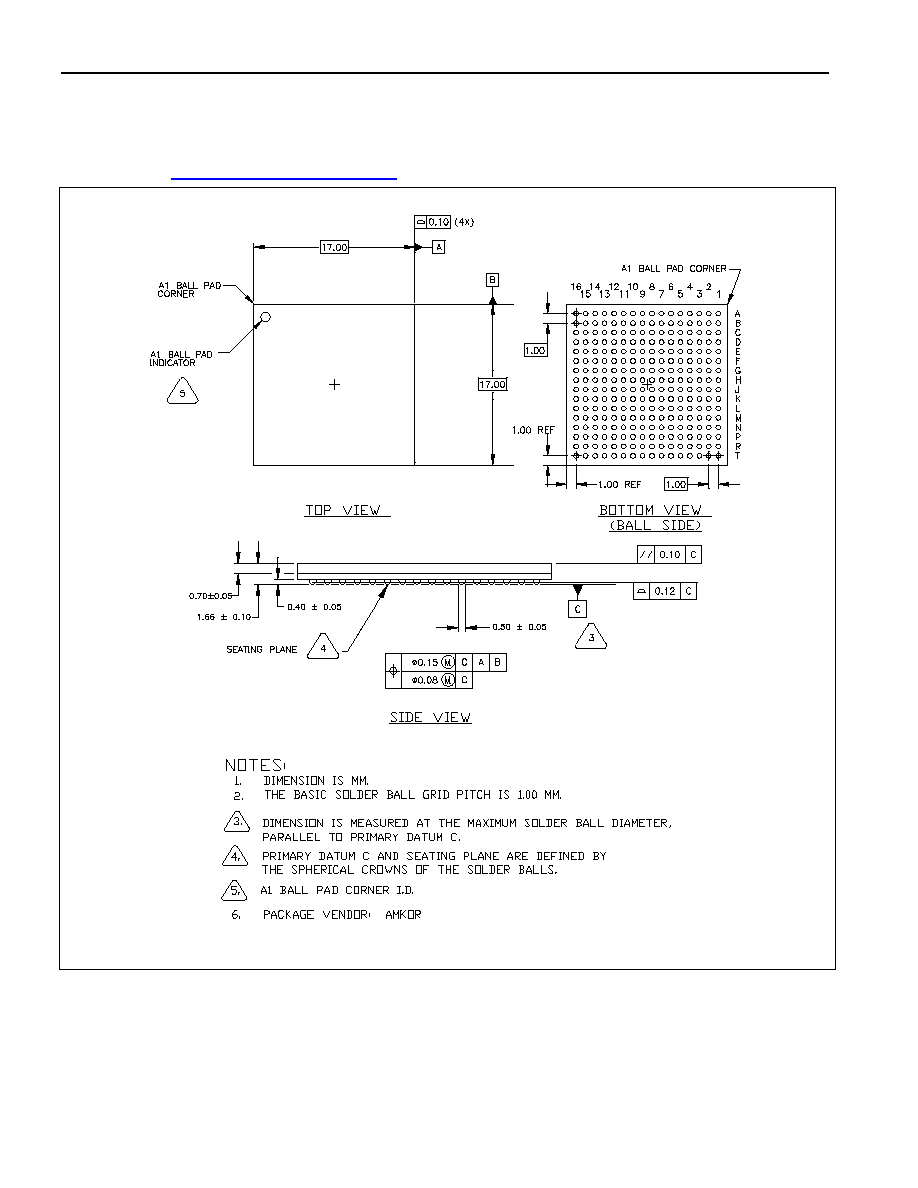
DS26324 3.3V, 16-Channel, E1/T1/J1, Short-Haul Line Interface Unit
110
of
112
11 PACKAGE INFORMATION
(The package drawing(s) in this data sheet may not reflect the most current specifications. For the latest package outline
information, go to
www.maxim-ic.com/DallasPackInfo
.)

DS26324 3.3V, 16-Channel, E1/T1/J1, Short-Haul Line Interface Unit
111
of
112
12 THERMAL INFORMATION
Table 12-1. Thermal Characteristics
PARAMETER MIN
TYP
MAX
V
(m/s)
NOTES
Power Dissipation in Package
1.4W
2.5W
3
Ambient Temperature
-40
∞C
+85
∞C
1
Junction Temperature
+125
∞C
Theta-JA (
q
JA
) in Still Air Conduction
+16.6
∞C/W
0 2
Theta-JC (
q
JC
) Conduction
+3.0
∞C/W
Theta-JB (
q
JB
) Conduction
+7.5
∞C/W
Theta-JA (
q
JA
) in Forced Air
+15.0
∞C/W
0.75
Theta-JA (
q
JA
) in Forced Air
+14.6
∞C/W
1.25
Theta-JA (
q
JA
) in Forced Air
+14.0
∞C/W
2.5
Note 1:
The package is mounted on a four-layer JEDEC standard test board.
Note 2:
Theta-JA (
q
JA
) is the junction-to-ambient thermal resistance, when the package is mounted on a four-layer JEDEC standard
test board.
Note 3:
The typical wattage is with 50% ones and LB00.

DS26324 3.3V, 16-Channel, E1/T1/J1, Short-Haul Line Interface Unit
112 of 112
Maxim/Dallas Semiconductor cannot assume responsibility for use of any circuitry other than circuitry entirely embodied in a Maxim/Dallas Semiconductor product.
No circuit patent licenses are implied. Maxim/Dallas Semiconductor reserves the right to change the circuitry and specifications without notice at any time.
Ma xi m I nt e gr at e d Pr o du ct s, 1 2 0 S a n G abr i el Dr i ve, S un n yv al e, C A 94 0 8 6 40 8- 7 37- 7 60 0
© 2005 Maxim Integrated Products
∑ Printed USA
The Maxim logo is a registered trademark of Maxim Integrated Products, Inc. The Dallas logo is a registered trademark of Dallas Semiconductor Corporation.
13 REVISION HISTORY
DATE DESCRIPTION
070105
Original release.