DS3070W
General Description
The DS3070W consists of a static RAM, a nonvolatile
(NV) controller, a year 2000-compliant real-time clock
(RTC), and an internal rechargeable manganese lithium
(ML) battery. These components are encased in a sur-
face-mount module with a 256-ball BGA footprint.
Whenever V
CC
is applied to the module, it recharges
the ML battery, powers the clock and SRAM from the
external power source, and allows the contents of the
clock registers or SRAM to be modified. When V
CC
is
powered down or out-of-tolerance, the controller write-
protects the memory contents and powers the clock
and SRAM from the battery. The DS3070W also con-
tains a power-supply monitor output (RST), as well as a
user-programmable interrupt output (IRQ/FT).
Applications
RAID Systems and Servers
Gaming
POS Terminals
Fire Alarms
Industrial Controllers
PLCs
Data-Acquisition Systems
Routers/Switches
Features
o Single-Piece, Reflowable, 27mm x 27mm BGA
Package Footprint
o Internal Manganese Lithium Battery and Charger
o Integrated Real-Time Clock
o Unconditionally Write-Protects the Clock and
SRAM when V
CC
is Out-of-Tolerance
o Automatically Switches to Battery Supply when
V
CC
Power Failures Occur
o Reset Output can be Used as a CPU Supervisor
o Interrupt Output can be Used as a CPU Watchdog
Timer
o Industrial Temperature Range (-40�C to +85�C)
o UL Recognized
DS3070W
3.3V Single-Piece 16Mb Nonvolatile SRAM
with Clock
______________________________________________ Maxim Integrated Products
1
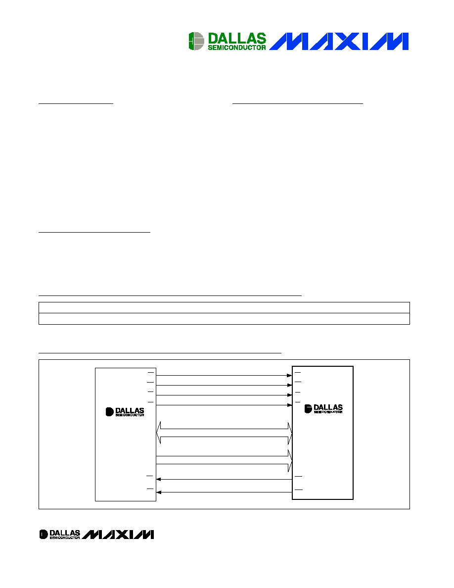
CE
DATA
ADDRESS
INT
RST
A0�20
DQ0�7
CE
21 BITS
8 BITS
MICROPROCESSOR
OR DSP
DS3070W
2048k x 8
NV SRAM
AND RTC
WR
WE
RD
OE
INT
IRQ/FT
CS
CS
Typical Operating Circuit
Rev 0; 6/06
For pricing, delivery, and ordering information, please contact Maxim/Dallas Direct! at
1-888-629-4642, or visit Maxim's website at www.maxim-ic.com.
Ordering Information
Pin Configuration appears at end of data sheet.
PART
TEMP RANGE
PIN-PACKAGE
SPEED
SUPPLY VOLTAGE
DS3070W-100#
-40�C to +85�C
256-ball 27mm x 27mm BGA Module
100ns
3.3V �0.3V
#Denotes a RoHS-compliant device that may include lead that is exempt under the RoHS requirements.
DS3070W
3.3V Single-Piece 16Mb Nonvolatile SRAM
with Clock
2
_____________________________________________________________________
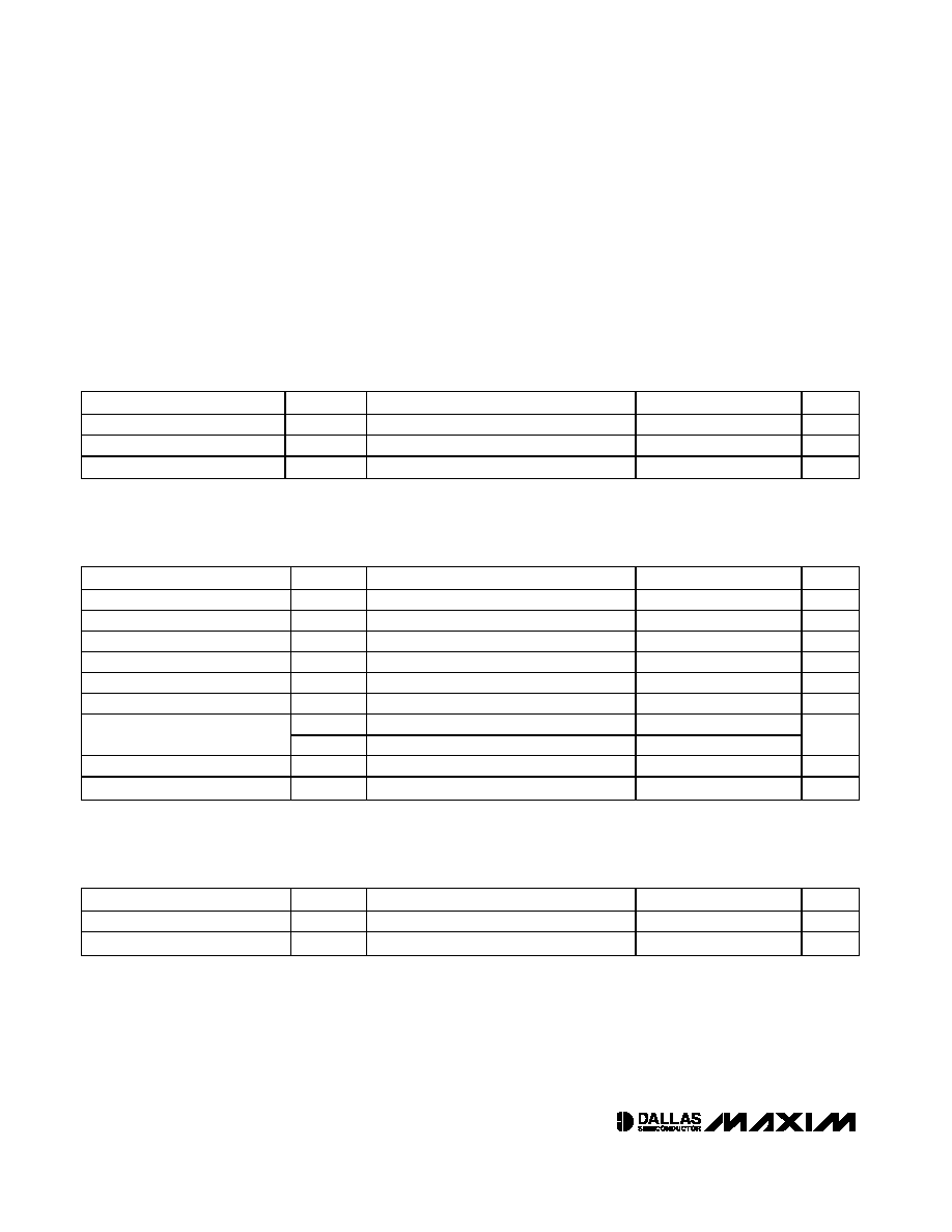
ABSOLUTE MAXIMUM RATINGS
RECOMMENDED OPERATING CONDITIONS
(T
A
= -40�C to +85�C.)
Stresses beyond those listed under "Absolute Maximum Ratings" may cause permanent damage to the device. These are stress ratings only, and functional
operation of the device at these or any other conditions beyond those indicated in the operational sections of the specifications is not implied. Exposure to
absolute maximum rating conditions for extended periods may affect device reliability.
Voltage Range on Any Pin Relative to Ground......-0.3V to +4.6V
Operating Temperature Range ...........................-40�C to +85�C
Storage Temperature Range ...............................-40�C to +85�C
Soldering Temperature Range..........See IPC/JEDEC J-STD-020
PARAMETER
SYMBOL
CONDITIONS
MIN
TYP
MAX
UNITS
Supply Voltage
V
CC
3.0
3.3
3.6
V
Input Logic 1
V
IH
2.2
V
CC
V
Input Logic 0
V
IL
0.0
0.4
V
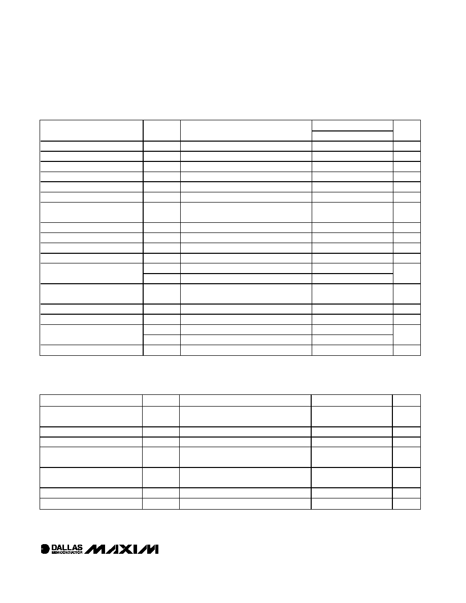
PIN CAPACITANCE
(T
A
= +25�C.)
PARAMETER
SYMBOL
CONDITIONS
MIN
TYP
MAX
UNITS
Input Capacitance
C
IN
Not production tested
15
pF
Input/Output Capacitance
C
OUT
Not production tested
15
pF
DC ELECTRICAL CHARACTERISTICS
(V
CC
= 3.3V �0.3V, T
A
= -40�C to +85�C.)
PARAMETER
SYMBOL
CONDITIONS
MIN
TYP
MAX
UNITS
Input Leakage Current
I
IL
-1.0
+1.0
�A
I/O Leakage Current
I
IO
CE = CS = V
CC
-1.0
+1.0
�A
Output-Current High
I
OH
At 2.4V
-1.0
mA
Output-Current Low
I
OL
At 0.4V
2.0
mA
Output-Current Low RST
I
OL
RST
At 0.4V (Note 1)
8.0
mA
Output-Current Low IRQ/FT
I
OL
IRQ/FT At 0.4V (Note 1)
7.0
mA
I
CCS1
CE = CS = 2.2V
0.5
7
Standby Current
I
CCS2
CE = CS = V
CC
- 0.2V
0.2
5
mA
Operating Current
I
CCO1
t
RC
= 200ns, outputs open
50
mA
Write Protection Voltage
V
TP
2.8
2.9
3.0
V
DS3070W
3.3V Single-Piece 16Mb Nonvolatile SRAM
with Clock
_____________________________________________________________________
3
AC ELECTRICAL CHARACTERISTICS
(V
CC
= 3.3V �0.3V, T
A
= -40�C to +85�C.)
DS3070W-100
PARAMETER
SYMBOL
CONDITIONS
MIN
MAX
UNITS
Read Cycle Time
t
RC
100
ns
Access Time
t
ACC
C
L
= 100pF
100
ns
OE to Output Valid
t
OE
50
ns
RTC OE to Output Valid
t
OEC
60
ns
CE or CS to Output Valid
t
CO
100
ns
OE or CE or CS to Output Active
t
COE
(Note 2)
5
ns
Output High Impedance from
Deselection
t
OD
(Note 2)
40
ns
Output Hold from Address
t
OH
5
ns
Write Cycle Time
t
WC
100
ns
Write Pulse Width
t
WP
(Note 3)
75
ns
Address Setup Time
t
AW
0
ns
t
WR1
(Note 4)
5
Write Recovery Time
t
WR2
(Note 5)
20
ns
Output High Impedance
from WE
t
ODW
(Note 2)
40
ns
Output Active from WE
t
OEW
(Note 2)
5
ns
Data Setup Time
t
DS
(Note 6)
40
ns
t
DH1
(Note 4)
0
Data Hold Time
t
DH2
(Note 5)
20
ns
Chip-to-Chip Setup Time
t
CCS
40
ns
POWER-DOWN/POWER-UP TIMING
(T
A
= -40�C to +85�C.)
PARAMETER
SYMBOL
CONDITIONS
MIN
TYP
MAX
UNITS
V
CC
Fail Detect to CE, CS, and
WE Inactive
t
PD
(Note 7)
1.5
�s
V
CC
Slew from V
TP
to 0V
t
F
150
�s
V
CC
Slew from 0V to V
TP
t
R
150
�s
V
CC
Valid to CE, CS, and WE
Inactive
t
PU
2
ms
V
CC
Valid to End of Write
Protection
t
REC
125
ms
V
CC
Fail Detect to RST Active
t
RPD
(Note 1)
3.0
�s
V
CC
Valid to RST Inactive
t
RPU
(Note 1)
40
350
525
ms
DS3070W
3.3V Single-Piece 16Mb Nonvolatile SRAM
with Clock
4
_____________________________________________________________________
Note 1:
IRQ/FT and RST are open-drain outputs and cannot source current. External pullup resistors should be connected to these
pins to realize a logic-high level.
Note 2:
These parameters are sampled with a 5pF load and are not 100% tested.
Note 3:
t
WP
is specified as the logical AND of CE with WE for SRAM writes, or CS with WE for RTC writes. t
WP
is measured from
the latter of the two related edges going low to the earlier of the two related edges going high.
Note 4:
t
WR1
and t
DH1
are measured from WE going high.
Note 5:
t
WR2
and t
DH2
are measured from CE going high for SRAM writes or CS going high for RTC writes.
Note 6:
t
DS
is measured from the earlier of CE or WE going high for SRAM writes, or from the earlier of CS or WE going high for
RTC writes.
Note 7:
In a power-down condition, the voltage on any pin may not exceed the voltage on V
CC
.
Note 8:
The expected t
DR
is defined as accumulative time in the absence of V
CC
starting from the time power is first applied by the
user. Minimum expected data-retention time is based upon a maximum of two +230�C convection reflow exposures, fol-
lowed by a fully charged cell. Full charge occurs with the initial application of V
CC
for a minimum of 96 hours. This parame-
ter is assured by component selection, process control, and design. It is not measured directly during production testing.
Note 9:
WE is high for any read cycle.
Note 10: OE = V
IH
or V
IL
. If OE = V
IH
during write cycle, the output buffers remain in a high-impedance state.
Note 11: If the CE or CS low transition occurs simultaneously with or latter than the WE low transition, the output buffers remain in a
high-impedance state during this period.
Note 12: If the CE or CS high transition occurs prior to or simultaneously with the WE high transition, the output buffers remain in a
high-impedance state during this period.
Note 13: If WE is low or the WE low transition occurs prior to or simultaneously with the related CE or CS low transition, the output
buffers remain in a high-impedance state during this period.
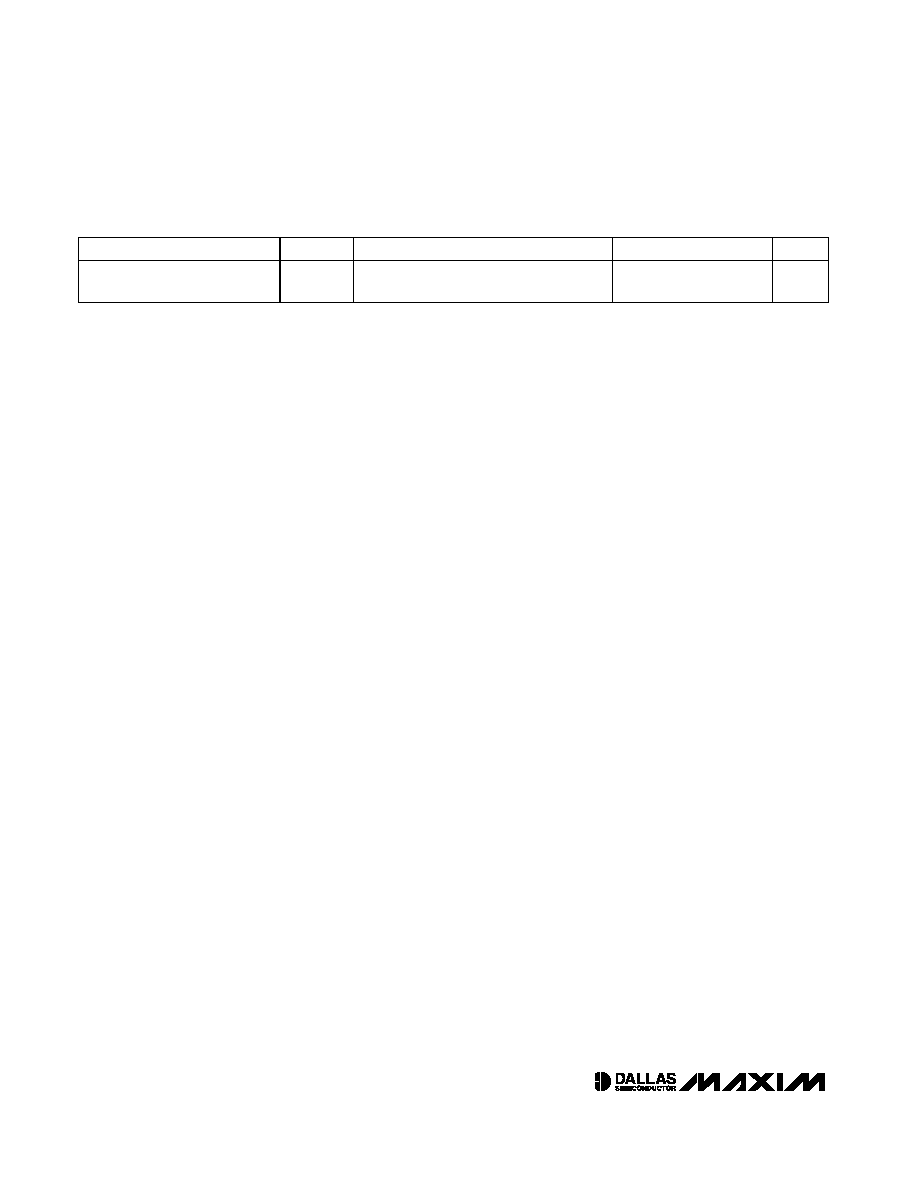
DATA RETENTION
(T
A
= +25�C.)
PARAMETER
SYMBOL
CONDITIONS
MIN
TYP
MAX
UNITS
Expected Data-Retention Time
(Per Charge)
t
DR
(Notes 7, 8)
2
3
years
DS3070W
3.3V Single-Piece 16Mb Nonvolatile SRAM
with Clock
_____________________________________________________________________
5
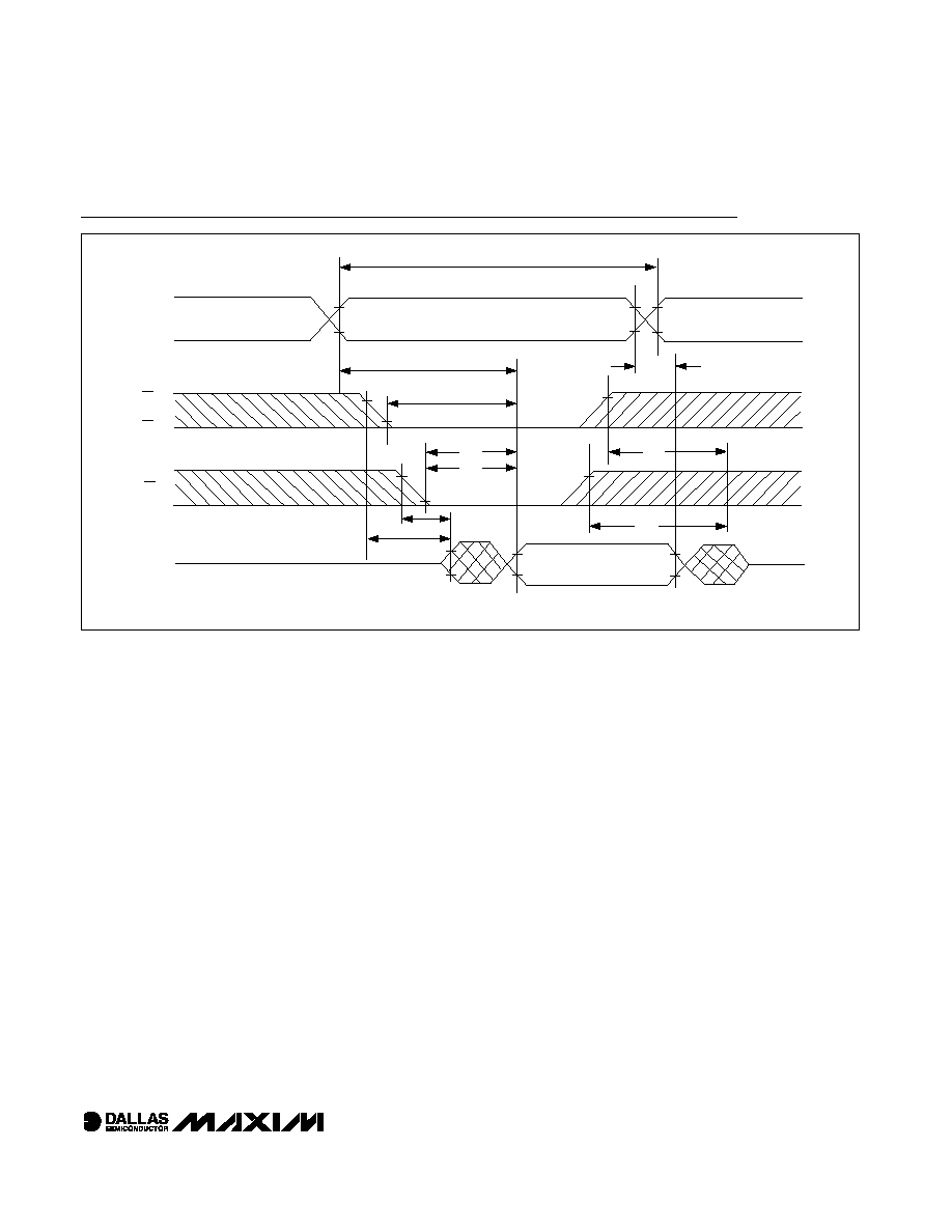
Read Cycle
OUTPUT
DATA VALID
t
RC
t
ACC
t
CO
t
OE
t
OEC
t
OH
t
OD
t
OD
t
COE
t
COE
V
IH
V
IH
V
IL
V
OH
V
OL
V
OH
V
OL
V
IL
V
IH
ADDRESSES
CE
OR
CS
OE
D
OUT
(SEE NOTE 9.)
V
IH
V
IH
V
IH
V
IH
V
IL
V
IL
V
IL