STANDARDS COMPLIANCE
1 of 130
REV: 062906
Note: Some revisions of this device may incorporate deviations from published specifications known as errata. Multiple revisions of any device
may be simultaneously available through various sales channels. For information about device errata, click here:
www.maxim-ic.com/errata
.
+
GENERAL DESCRIPTION
The DS32506 (6 port), DS32508 (8 port), and
DS32512 (12 port) line interface units (LIUs) are
highly integrated, low-power, feature-rich LIUs for
DS3, E3, and STS-1 applications. Each LIU port in
these devices has independent receive and transmit
paths, a jitter attenuator, full-featured pattern
generator and detector, performance-monitoring
counters, and a complete set of loopbacks. An on-
chip clock adapter generates all line-rate clocks from
a single input clock. Ports are independently software
configurable for DS3, E3, and STS-1 and can be
individually powered down. Control interface options
include 8-bit parallel, SPI, and hardware mode.
APPLICATIONS
SONET/SDH and PDH
Multiplexers
Digital Cross-
Connects
Access Concentrators
ATM and Frame Relay
Equipment
CSUs/DSUs
PBXs
WAN Routers and
Switches
DSLAMs
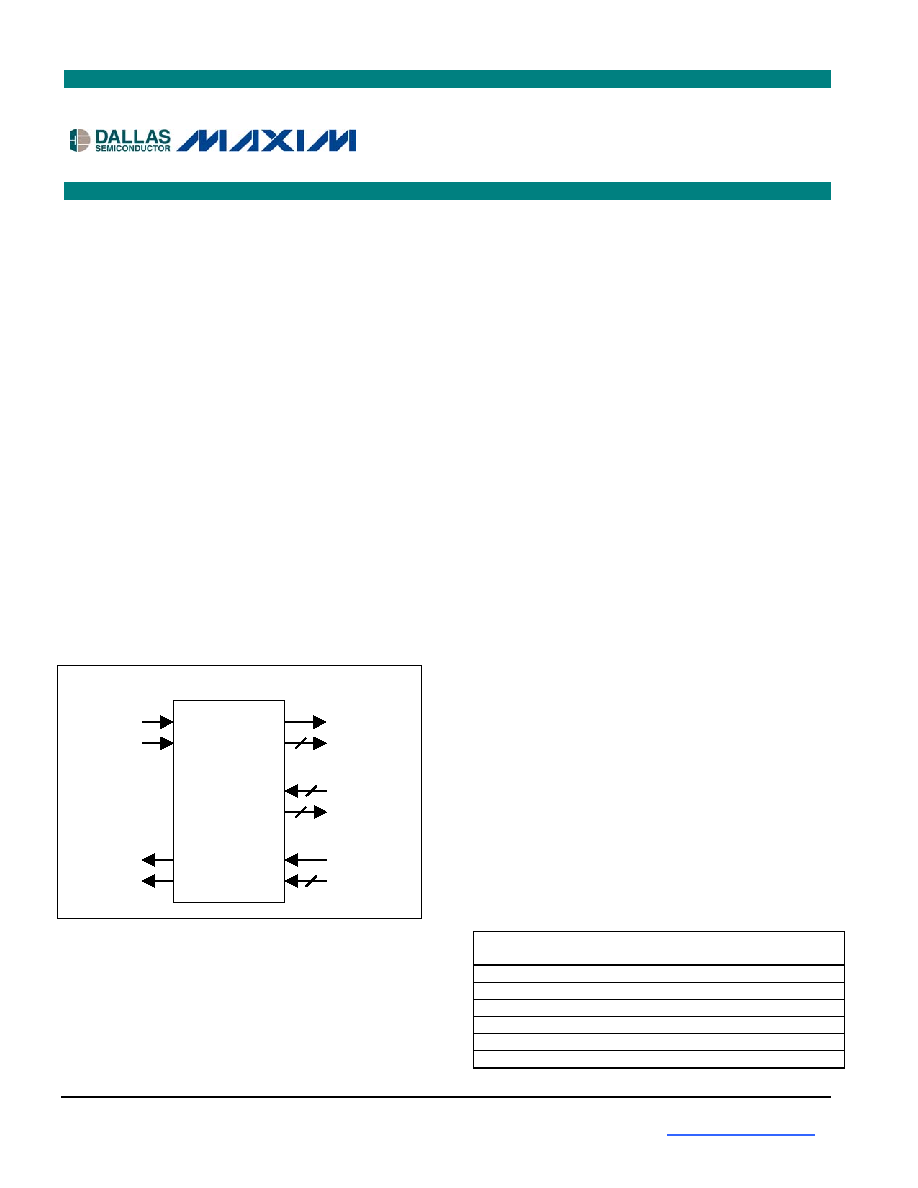
FUNCTIONAL DIAGRAM
FEATURES
Pin-Compatible Family of Products
Each Port Independently Configurable
Receive Clock and Data Recovery for Up to 457
meters (1500 feet) of 75
Coaxial Cable
Standards-Compliant Transmit Waveshaping
Uses 1:1 Transformers on Both Tx and Rx
Three Control Interface Options: 8/16-Bit
Parallel, SPI, and Hardware Mode
Jitter Attenuators (One Per Port) Can be Placed
in the Receive Path or the Transmit Path
Jitter Attenuators Have Provisionable Buffer
Depth: 16, 32, 64, or 128 bits
Built-In Clock Adapter Generates All Line-Rate
Clocks from a Single Input Clock (DS3, E3, STS-1,
12.8MHz, 19.44MHz, 38.88MHz, 77.76MHz)
Per-Port Programmable Internal Line Termination
Requiring Only External Transformers
High-Impedance Tx and Rx, Even When V
DD
= 0,
Enables Hot-Swappable, 1:1 and 1+1 Board
Redundancy Without Relays
Per-Port BERT for PRBS and Repetitive Pattern
Generation and Detection
Tx and Rx Open and Short Detection Circuitry
Transmit Driver Monitor Circuitry
Receive Loss-of-Signal (LOS) Monitoring
Compliant with ANSI T1.231 and ITU G.775
Automatic Data Squelching on Receive LOS
Large Line Code Performance-Monitoring
Counters for Accumulation Intervals Up to 1s
Local and Remote Loopbacks
Transmit Common Clock Option
Power-Down Capability for Unused Ports
Low-Power 1.8V/3.3V Operation (5V Tolerant
I/O)
Industrial Temperature Range: -40�C to +85
�C
Small Package: 23mm x 23mm, 484-Pin BGA
IEEE 1149.1 JTAG Support
ORDERING INFORMATION
PART LIUs
TEMP
RANGE
PIN-
PACKAGE
DS32506
6
0�C to +70�C
484 BGA
DS32506N
6
-40�C to +85�C 484 BGA
DS32508
8
0�C to +70�C
484 BGA
DS32508N
8
-40�C to +85�C 484 BGA
DS32512
12
0�C to +70�C
484 BGA
DS32512N
12
-40�C to +85�C 484 BGA
Note: Add the "+" suffix for the lead-free package option.
DS32506/DS32508/DS32512
6-/8-/12-Port DS3/E3/STS-1 LIU
www.maxim-ic.com
RECEIVE
CLOCK
AND DATA
Dallas
Semiconductor
DS325xx
CLK
DATA
CLK
DATA
TRANSMIT
CLOCK
AND DATA
CONTROL
AND
STATUS
TXP
TXN
RXP
RXN
EACH LIU
LINE IN
DS3, E3,
OR STS-1
LINE OUT
DS3, E3,
OR STS-1

DS32506/DS32508/DS32512
2 of 130
TABLE OF CONTENTS
1.
STANDARDS COMPLIANCE .............................................................................................6
2.
BLOCK DIAGRAM ..............................................................................................................7
3.
APPLICATION EXAMPLE ..................................................................................................8
4.
DETAILED DESCRIPTION..................................................................................................9
5.
DETAILED FEATURES.....................................................................................................11
5.1
G
LOBAL
F
EATURES
.......................................................................................................................11
5.2
R
ECEIVER
.....................................................................................................................................11
5.3
T
RANSMITTER
...............................................................................................................................11
5.4
J
ITTER
A
TTENUATOR
.....................................................................................................................11
5.5
B
IT
E
RROR
-R
ATE
T
ESTER
(BERT) F
EATURES
...............................................................................12
5.6
C
LOCK
A
DAPTER
...........................................................................................................................12
5.7
P
ARALLEL
M
ICROPROCESSOR
I
NTERFACE
F
EATURES
.....................................................................12
5.8
SPI S
ERIAL
M
ICROPROCESSOR
I
NTERFACE
F
EATURES
..................................................................12
5.9
M
ISCELLANEOUS
F
EATURES
..........................................................................................................12
5.10
T
EST
F
EATURES
............................................................................................................................12
5.11
L
OOPBACK
F
EATURES
...................................................................................................................12
6.
CONTROL INTERFACE MODES......................................................................................13
7.
PIN DESCRIPTIONS .........................................................................................................14
7.1
S
HORT
P
IN
D
ESCRIPTIONS
............................................................................................................14
7.2
D
ETAILED
P
IN
D
ESCRIPTIONS
........................................................................................................17
8.
FUNCTIONAL DESCRIPTION ..........................................................................................24
8.1
LIU M
ODE
....................................................................................................................................24
8.2
T
RANSMITTER
...............................................................................................................................24
8.2.1
Transmit Clock .................................................................................................................................... 24
8.2.2
Framer Interface Format and the B3ZS/HDB3 Encoder..................................................................... 24
8.2.3
Error Insertion ..................................................................................................................................... 24
8.2.4
AIS Generation.................................................................................................................................... 25
8.2.5
Waveshaping ...................................................................................................................................... 25
8.2.6
Line Build-Out ..................................................................................................................................... 25
8.2.7
Line Driver........................................................................................................................................... 25
8.2.8
Interfacing to the Line ......................................................................................................................... 25
8.2.9
Driver Monitor and Output Failure Detection ...................................................................................... 26
8.2.10
Power-Down........................................................................................................................................ 26
8.2.11
Jitter Generation (Intrinsic).................................................................................................................. 26
8.2.12
Jitter Transfer ...................................................................................................................................... 26
8.3
R
ECEIVER
.....................................................................................................................................30
8.3.1
Interfacing to the Line ......................................................................................................................... 30
8.3.2
Optional Preamp ................................................................................................................................. 30
8.3.3
Automatic Gain Control (AGC) and Adaptive Equalizer ..................................................................... 30
8.3.4
Clock and Data Recovery (CDR) ........................................................................................................ 31
8.3.5
Loss-of-Signal (LOS) Detector............................................................................................................ 31
8.3.6
Framer Interface Format and the B3ZS/HDB3 Decoder .................................................................... 32
8.3.7
Power-Down........................................................................................................................................ 33
8.3.8
Input Failure Detection........................................................................................................................ 33
8.3.9
Jitter and Wander Tolerance............................................................................................................... 34
8.3.10
Jitter Transfer ...................................................................................................................................... 35
8.4
J
ITTER
A
TTENUATOR
.....................................................................................................................35
8.5
BERT...........................................................................................................................................36

DS32506/DS32508/DS32512
3 of 130
8.5.1
Configuration and Monitoring.............................................................................................................. 36
8.5.2
Receive Pattern Detection .................................................................................................................. 37
8.5.3
Transmit Pattern Generation............................................................................................................... 39
8.6
L
OOPBACKS
..................................................................................................................................40
8.7
G
LOBAL
R
ESOURCES
....................................................................................................................40
8.7.1
Clock Rate Adapter (CLAD)................................................................................................................ 40
8.7.2
One-Second Reference Generator..................................................................................................... 41
8.7.3
General-Purpose I/O Pins................................................................................................................... 42
8.7.4
Performance Monitor Register Update ............................................................................................... 42
8.7.5
Transmit Manual Error Insertion ......................................................................................................... 43
8.8
8-/16-B
IT
P
ARALLEL
M
ICROPROCESSOR
I
NTERFACE
......................................................................43
8.8.1
8-Bit and 16-Bit Bus Widths ................................................................................................................ 43
8.8.2
Byte Swap Mode................................................................................................................................. 43
8.8.3
Read-Write And Data Strobe Modes .................................................................................................. 43
8.8.4
Multiplexed and Nonmultiplexed Operation ........................................................................................ 43
8.8.5
Clear-On-Read And Clear-On-Write Modes ....................................................................................... 44
8.8.6
Global Write Mode .............................................................................................................................. 44
8.9
SPI S
ERIAL
M
ICROPROCESSOR
I
NTERFACE
...................................................................................44
8.10
I
NTERRUPT
S
TRUCTURE
................................................................................................................46
8.11
R
ESET AND
P
OWER
-D
OWN
............................................................................................................47
8.12
I
NITIALIZATION
...............................................................................................................................48
9.
REGISTER MAPS AND DESCRIPTIONS.........................................................................49
9.1
O
VERVIEW
....................................................................................................................................49
9.1.1
Status Bits ........................................................................................................................................... 49
9.1.2
Configuration Fields ............................................................................................................................ 49
9.1.3
Counters.............................................................................................................................................. 49
9.2
O
VERALL
R
EGISTER
M
AP
..............................................................................................................50
9.3
G
LOBAL
R
EGISTERS
......................................................................................................................51
9.4
P
ORT
C
OMMON
R
EGISTERS
..........................................................................................................62
9.5
LIU R
EGISTERS
............................................................................................................................70
9.6
B3ZS/HDB3 E
NCODER
R
EGISTERS
..............................................................................................79
9.7
B3ZS/HDB3 D
ECODER
R
EGISTERS
..............................................................................................80
9.8
BERT R
EGISTERS
........................................................................................................................84
10.
JTAG INFORMATION ...................................................................................................91
11.
ELECTRICAL CHARACTERISTICS .............................................................................92
12.
PIN ASSIGNMENTS....................................................................................................106
13.
PACKAGE INFORMATION.........................................................................................127
13.1
484-L
EAD
BGA (23
MM X
23
MM
) (56-G60038-001) .....................................................................127
14.
THERMAL INFORMATION .........................................................................................128
15.
ACRONYMS AND ABBREVIATIONS.........................................................................129
16.
TRADEMARK ACKNOWLEDGEMENTS....................................................................129
17.
DATA SHEET REVISION HISTORY ...........................................................................130

DS32506/DS32508/DS32512
4 of 130
LIST OF FIGURES
Figure 2-1. Block Diagram ........................................................................................................................................... 7
Figure 3-1. 12-Port Unchannelized DS3/E3 Card ....................................................................................................... 8
Figure 4-1. External Connections, Internal Termination Enabled................................................................................ 9
Figure 4-2. External Connections, Internal Termination Disabled............................................................................. 10
Figure 8-1. DS3 Waveform Template........................................................................................................................ 27
Figure 8-2. STS-1 Waveform Template..................................................................................................................... 28
Figure 8-3. E3 Waveform Template........................................................................................................................... 29
Figure 8-4. STS-1 and E3 Jitter Tolerance............................................................................................................... 34
Figure 8-5. DS3 Jitter Tolerance............................................................................................................................... 34
Figure 8-6. DS3 and E3 Wander Tolerance ............................................................................................................. 35
Figure 8-7. Jitter Attenuation/Jitter Transfer .............................................................................................................. 36
Figure 8-8. PRBS Synchronization State Diagram.................................................................................................... 38
Figure 8-9. Repetitive Pattern Synchronization State Diagram................................................................................. 39
Figure 8-10. SPI Clock Polarity and Phase Options.................................................................................................. 45
Figure 8-11. SPI Bus Transactions............................................................................................................................ 46
Figure 8-12. Interrupt Signal Flow ............................................................................................................................. 47
Figure 11-1. Transmitter Framer Interface Timing Diagram...................................................................................... 95
Figure 11-2. Receiver Framer Interface Timing Diagram.......................................................................................... 95
Figure 11-3. Parallel CPU Interface Intel Read Timing Diagram (Nonmultiplexed) .................................................. 99
Figure 11-4. Parallel CPU Interface Intel Write Timing Diagram (Nonmultiplexed) .................................................. 99
Figure 11-5. Parallel CPU Interface Motorola Read Timing Diagram (Nonmultiplexed) ......................................... 100
Figure 11-6. Parallel CPU Interface Motorola Write Timing Diagram (Nonmultiplexed) ......................................... 100
Figure 11-7. Parallel CPU Interface Intel Read Timing Diagram (Multiplexed)....................................................... 101
Figure 11-8. Parallel CPU Interface Intel Write Timing Diagram (Multiplexed) ....................................................... 101
Figure 11-9. Parallel CPU Interface Motorola Read Timing Diagram (Multiplexed)................................................ 102
Figure 11-10. Parallel CPU Interface Motorola Write Timing Diagram (Multiplexed).............................................. 102
Figure 11-11. SPI Interface Timing Diagram ........................................................................................................... 104
Figure 11-12. JTAG Timing Diagram....................................................................................................................... 105
Figure 12-1. DS32512 Pin Assignment, Hardware and Microprocessor Interfaces................................................ 109
Figure 12-2. DS32512 Pin Assignment, Hardware Interface Only .......................................................................... 111
Figure 12-3. DS32512 Pin Assignment, Microprocessor Interface Only ................................................................. 113
Figure 12-4. DS32508 Pin Assignment, Hardware and Microprocessor Interfaces................................................ 115
Figure 12-5. DS32508 Pin Assignment, Hardware Interface Only .......................................................................... 117
Figure 12-6. DS32508 Pin Assignment, Microprocessor Interface Only ................................................................. 119
Figure 12-7. DS32506 Pin Assignment, Hardware and Microprocessor Interfaces................................................ 121
Figure 12-8. DS32506 Pin Assignment, Hardware Interface Only .......................................................................... 123
Figure 12-9. DS32506 Pin Assignment, Microprocessor Interface Only ................................................................. 125

DS32506/DS32508/DS32512
5 of 130
LIST OF TABLES
Table 1-1. Applicable Telecommunications Standards ............................................................................................... 6
Table 7-1. Short Pin Descriptions .............................................................................................................................. 14
Table 7-2. Analog Line Interface Pin Descriptions .................................................................................................... 17
Table 7-3. Digital Framer Interface Pin Descriptions................................................................................................. 17
Table 7-4. Global Pin Descriptions ............................................................................................................................ 18
Table 7-5. Hardware Interface Pin Descriptions........................................................................................................ 19
Table 7-6. Parallel Interface Pin Descriptions ........................................................................................................... 21
Table 7-7. SPI Serial Interface Pin Descriptions ....................................................................................................... 22
Table 7-8. CLAD Pin Descriptions ............................................................................................................................. 22
Table 7-9. JTAG Pin Descriptions ............................................................................................................................. 23
Table 7-10. Power-Supply Pin Descriptions .............................................................................................................. 23
Table 7-11. Manufacturing Test Pin Descriptions...................................................................................................... 23
Table 8-1. Jitter Generation ....................................................................................................................................... 26
Table 8-2. DS3 Waveform Equations ........................................................................................................................ 27
Table 8-3. DS3 Waveform Test Parameters and Limits ............................................................................................ 27
Table 8-4. STS-1 Waveform Equations..................................................................................................................... 28
Table 8-5. STS-1 Waveform Test Parameters and Limits......................................................................................... 28
Table 8-6. E3 Waveform Test Parameters and Limits............................................................................................... 29
Table 8-7. Transformer Characteristics ..................................................................................................................... 30
Table 8-8. Recommended Transformers................................................................................................................... 30
Table 8-9. Pseudorandom Pattern Generation.......................................................................................................... 37
Table 8-10. Repetitive Pattern Generation ................................................................................................................ 37
Table 8-11. CLAD Clock Source Settings ................................................................................................................. 41
Table 8-12. CLAD Clock Pin Output Settings............................................................................................................ 41
Table 8-13. Global One-Second Reference Source.................................................................................................. 41
Table 8-14. GPIO Pin Global Signal Assignments .................................................................................................... 42
Table 8-15. GPIO Pin Control.................................................................................................................................... 42
Table 8-16. Reset and Power-Down Sources ........................................................................................................... 48
Table 9-1. Overall Register Map................................................................................................................................ 50
Table 9-2. Port Registers........................................................................................................................................... 50
Table 9-3. Global Register Map................................................................................................................................. 51
Table 9-4. Port Common Register Map..................................................................................................................... 62
Table 10-1. JTAG ID Code ........................................................................................................................................ 91
Table 11-1. Recommended DC Operating Conditions.............................................................................................. 92
Table 11-2. DC Characteristics.................................................................................................................................. 93
Table 11-3. Framer Interface Timing ......................................................................................................................... 94
Table 11-4. Receiver Input Characteristics--DS3 and STS-1 Modes....................................................................... 96
Table 11-5. Receiver Input Characteristics--E3 Mode ............................................................................................. 96
Table 11-6. Transmitter Output Characteristics--DS3 and STS-1 Modes................................................................ 97
Table 11-7. Transmitter Output Characteristics--E3 Mode....................................................................................... 97
Table 11-8. Parallel CPU Interface Timing ................................................................................................................ 98
Table 11-9. SPI Interface Timing ............................................................................................................................. 103
Table 11-10. JTAG Interface Timing........................................................................................................................ 105
Table 12-1. Pin Assignments Sorted by Signal Name for DS32506/DS32508/DS32512 ....................................... 106
Table 14-1. Thermal Properties, Natural Convection .............................................................................................. 128
Table 14-2. Theta-JA (
JA
) vs. Airflow...................................................................................................................... 128
Document Outline