 | ÐлекÑÑоннÑй компоненÑ: DS4510U-5 | СкаÑаÑÑ:  PDF PDF  ZIP ZIP |
Äîêóìåíòàöèÿ è îïèñàíèÿ www.docs.chipfind.ru
General Description
The DS4510 is a CPU supervisor with integrated 64-
byte EEPROM memory and four programmable, non-
volatile (NV) I/O pins. It is configured with an
industry-standard I
2
CTM interface using either fast-
mode (400kbps) or standard-mode (100kbps) commu-
nication. The I/O pins can be used as general-purpose
I
2
C-to-parallel I/O expander with unlimited read/write
capability. EEPROM registers allow the power-on value
of the I/O pins to be adjusted to keep track of the sys-
tem's state through power cycles, and the CPU supervi-
sor's timer can be adjusted between 125ms and
1000ms to meet most any application need.
Applications
RAM-Based FPGA Bank Switching for
Multiple Profiles
Industrial Controls
Cellular Telephones
PC Peripherals
PDAs
Features
Accurate 5%, 10%, or 15% 5V Power-Supply
Monitoring
Programmable Reset Timer Maintains Reset After
V
CC
Returns to an In-Tolerance Condition
Four Programmable, NV, Digital I/O Pins with
Selectable Internal Pullup Resistor
64 Bytes of User EEPROM
Reduces Need for Discrete Components
I
2
C-Compatible Serial Interface
10-Pin µSOP Package
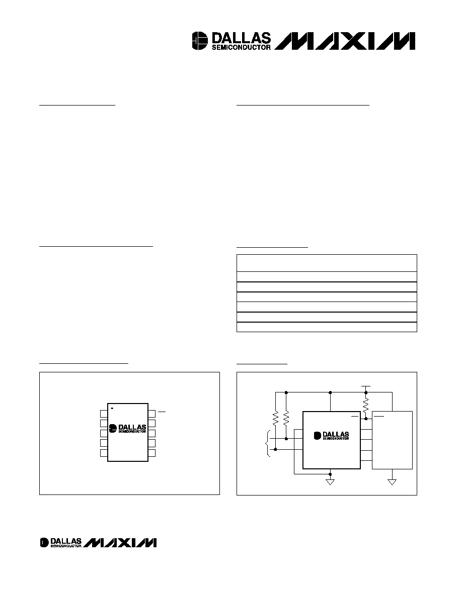
DS4510
CPU Supervisor with Nonvolatile Memory and
Programmable I/O
______________________________________________ Maxim Integrated Products
1
1
2
3
4
5
10
9
8
7
6
I/O
0
I/O
1
I/O
2
V
CC
SCL
SDA
A
0
TOP VIEW
I/O
3
GND
µ
SOP
DS4510
RST
Pin Configuration
Ordering Information
DS4510
A0
SDA
SCL
I/O
0
I/O
1
I/O
2
I/O
3
GND
V
CC
V
CC
FPGA
2.7V TO 5.5V
GND
RESET
CONFIG0
CONFIG1
CONFIG2
CONFIG3
FROM
SYSTEM
CONTROLLER
4.7k
4.7k
4.7k
RST
Typical Operating Circuit
Rev 2; 8/04
For pricing, delivery, and ordering information, please contact Maxim/Dallas Direct! at
1-888-629-4642, or visit Maxim's website at www.maxim-ic.com.
PART
V
CC
TRIP
POINT
TEMP RANGE
PIN-
PACKAGE
DS4510U-5
5%
-40°C to +85°C
10 µSOP
DS4510U-10
10%
-40°C to +85°C
10 µSOP
DS4510U-15
15%
-40°C to +85°C
10 µSOP
DS4510U-5/T&R
5%
-40°C to +85°C
10 µSOP
DS4510U-10/T&R
10%
-40°C to +85°C
10 µSOP
DS4510U-15/T&R
15%
-40°C to +85°C
10 µSOP
I
2
C is a registered trademark of Philips Corp. Purchase of I
2
C components of Maxim Integrated Products, Inc. or one of its
Associated Companies, conveys a license under the Philips I
2
C Patent Rights to use these components in an I
2
C system, provided
the system conforms to the I
2
C Standard Specifications as defined by Philips.
DS4510
CPU Supervisor with Nonvolatile Memory and
Programmable I/O
2
_____________________________________________________________________
ABSOLUTE MAXIMUM RATINGS
RECOMMENDED DC OPERATING CONDITIONS
(T
A
= -40°C to +85°C)
Stresses beyond those listed under "Absolute Maximum Ratings" may cause permanent damage to the device. These are stress ratings only, and functional
operation of the device at these or any other conditions beyond those indicated in the operational sections of the specifications is not implied. Exposure to
absolute maximum rating conditions for extended periods may affect device reliability.
Voltage Range on V
CC
, SDA, and SCL
Pins Relative to Ground.....................................-0.5V to +6.0V
Voltage Range on A
0
, I/O
0
, I/O
1
, I/O
2
, I/O
3
Relative
to Ground ..............-0.5V to V
CC
+ 0.5V, not to exceed +6.0V.
Operating Temperature Range ...........................-40
°C to +85°C
EEPROM Programming Temperature .....................0
°C to +70°C
Storage Temperature Range .............................-55
°C to +125°C
Soldering Temperature .......................................See IPC/JEDEC
J-STD-020A Specification
PARAMETER
SYMBOL
CONDITIONS
MIN
TYP
MAX
UNITS
Supply Voltage
V
CC
(Notes 1)
2.7
5.5
V
Input Logic 1
V
IH
(Note 2)
0.7 x V
CC
V
CC
+ 0.3
V
Input Logic 0
V
IL
-0.3
+0.3 x V
CC
V
DC ELECTRICAL CHARACTERISTICS
(V
CC
= 2.7V to 5.5V, T
A
= -40°C to +85°C.)
PARAMETER
SYMBOL
CONDITIONS
MIN
TYP
MAX
UNITS
DS4510U-5
4.5
4.625
4.75
DS4510U-10
4.25
4.375
4.49
V
CC
Trip Point
V
CCTP
DS4510U-15
4.0
4.125
4.24
V
Standby Current
I
STBY
V
CC
= 5.0V (Note 3)
50
75
µA
Input Leakage
I
L
-1.0
+1.0
µA
3mA sink current
0.4
SDA Low-Level Output Voltage
V
OL
6mA sink current
0.6
V
I/O
X
Low-Level Output Voltage
V
OLIOX
4mA sink current
0.4
V
RST Pin Low-Level Output
V
OL
RST
10mA sink current (Note 4)
0.4
V
I/O
X
Pullup Resistors
R
P
4.0
5.0
6.5
k
I/O Capacitance
C
I/O
(Note 5)
10
pF
DS4510
CPU Supervisor with Nonvolatile Memory and
Programmable I/O
_____________________________________________________________________
3
CPU SUPERVISOR AC ELECTRICAL CHARACTERISTICS (See
Figure
1)
(V
CC
= 2.7V to 5.5V, T
A
= -40°C to +85°C.)
PARAMETER
SYMBOL
CONDITIONS
MIN
TYP
MAX
UNITS
TD1= 0, TD0 = 0
112
125
138
TD1= 0, TD0 = 1
225
250
275
TD1= 1, TD0 = 0
450
500
550
RST Active Time
t
RST
TD1= 1, TD0 = 1
900
1000
1100
ms
TD1= 0, TD0 = 0
112
125
138
TD1= 0, TD0 = 1
225
250
275
TD1= 1, TD0 = 0
450
500
550
V
CC
Detect to
RST
t
RPU
TD1= 1, TD0 = 1
900
1000
1100
ms
V
CC
Fail to
RST
t
RPD
4
10
µs
AC ELECTRICAL CHARACTERISTICS (See
Figure
5)
(V
CC
= 2.7V to 5.5V, T
A
= -40°C to +85°C, timing referenced to V
IL(MAX) and
V
IH(MIN).)
PARAMETER
SYMBOL
CONDITIONS
MIN
TYP
MAX
UNITS
SCL Clock Frequency
f
SCL
(Note 6)
0
400
kHz
Bus Free Time Between Stop and
Start Conditions
t
BUF
1.3
µs
Hold Time (Repeated) Start
Condition
t
HD:STA
0.6
µs
Low Period of SCL
t
LOW
1.3
µs
High Period of SCL
t
HIGH
0.6
µs
Data Hold Time
t
HD:DAT
0
0.9
µs
Data Setup Time
t
SU:DAT
100
ns
Start Setup time
t
SU:STA
0.6
µs
SDA and SCL Rise Time
t
R
(Note 7)
20 + 0.1C
B
300
ns
SDA and SCL Fall Time
t
F
(Note 7)
20 + 0.1C
B
300
ns
Stop Setup Time
t
SU:STO
0.6
µs
SDA and SCL Capacitive
Loading
C
B
(Note 7)
400
pF
EEPROM Write Time
t
W
(Note 7)
10
20
ms
DS4510
CPU Supervisor with Nonvolatile Memory and
Programmable I/O
4
_____________________________________________________________________
Note 1:
All voltages referenced to ground.
Note 2:
The DS4510 does not obstruct the SDA and SCL lines if V
CC
is switched off, as long as the voltages applied to these
inputs do not violate their min and max input voltage levels.
Note 3:
ISTBY specified with V
CC
equal to 5.0V, and control port-logic pins are driven to ground or V
CC
for the corresponding
inactive state (SDA = SCL = V
CC
), does not include pullup resistor current.
Note 4:
See Typical Operating Characteristics for the
RST output voltage vs. supply voltage.
Note 5:
This parameter is guaranteed by design.
Note 6:
I
2
C interface timing shown for is for fast-mode (400kHz) operation. This device is also backward compatible with I
2
C
standard-mode timing.
Note 7:
CB--total capacitance of one bus line in picofarads.
Note 8:
EEPROM write time applies to all the EEPROM memory and SEEPROM memory when
SEE = 0. The EEPROM write time
begins at the occurrence of a stop condition.
NONVOLATILE MEMORY CHARACTERISTICS
(V
CC
=
2.7V
to 5.5V, T
A
= 0°C to +70°C.)
PARAMETER
SYMBOL
CONDITIONS
MIN
TYP
MAX
UNITS
Writes
+70°C (Note 5)
50,000
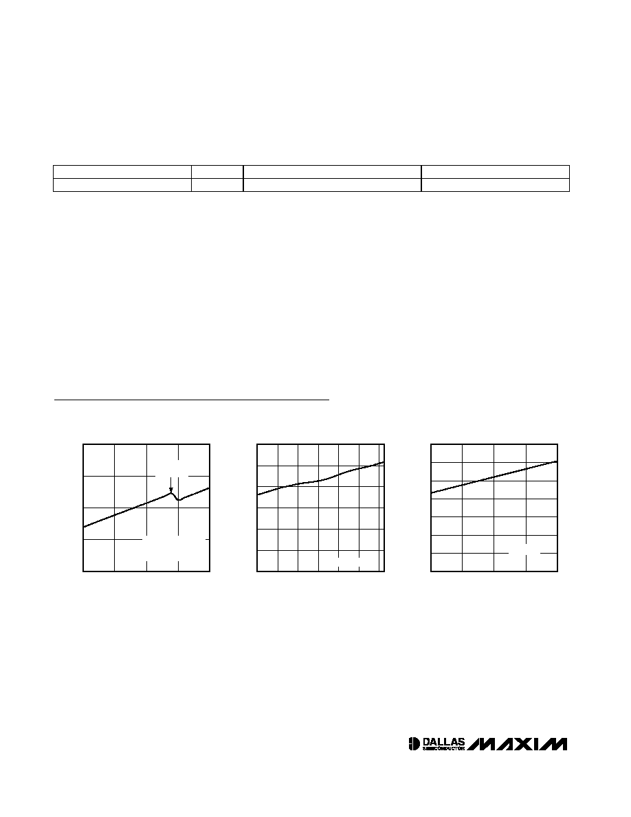
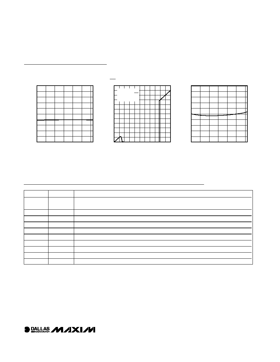
Typical Operating Characteristics
(V
CC
= +5.0V, T
A
= +25°C, unless otherwise noted.)
SUPPLY CURRENT vs. SUPPLY VOLTAGE
DS4510 toc01
SUPPLY VOLTAGE (V)
SUPPLY CURRENT (
µ
A)
4.5
4.0
3.5
35
40
45
50
30
3.0
5.0
V
CC
(10%)
TRIP POINT
SDA = SCL = V
CC
I/O CONTROL BITS = 0
I/O PULLUPS DISABLED
SUPPLY CURRENT vs. TEMPERATURE
DS4510 toc02
TEMPERATURE (
°C)
SUPPLY CURRENT (
µ
A)
60
40
20
0
-20
10
20
30
40
50
60
0
-40
80
SDA = SCL = V
CC
SUPPLY CURRENT vs. SCL FREQUENCY
DS4510 toc03
SCL FREQUENCY (kHz)
SUPPLY CURRENT (
µ
A)
300
200
100
10
20
30
40
50
60
70
0
0
400
SDA = V
CC
DS4510
CPU Supervisor with Nonvolatile Memory and
Programmable I/O
_____________________________________________________________________
5
Typical Operating Characteristics (continued)
(V
CC
= +5.0V, T
A
= +25°C, unless otherwise noted.)
V
CC
TRIP POINT vs. TEMPERATURE
DS4510 toc04
TEMPERATURE (
°C)
V
CC
TRIP POINT (V)
60
40
20
0
-20
4.1
4.2
4.3
4.4
4.5
4.6
4.7
4.8
4.9
5.0
4.0
-40
80
RST OUTPUT VOLTAGE vs. SUPPLY VOLTAGE
DS4510 toc05
SUPPLY VOLTAGE (V)
RESET TRIP VOLTAGE (V)
5.0
4.5
3.5 4.0
1.0 1.5 2.0 2.5 3.0
0.5
0.5
1.0
1.5
2.0
2.5
3.0
3.5
4.0
4.5
5.0
5.5
6.0
0
0
5.5
5.6k
PULLUP
RESISTOR ON RST
SDA = SCL = V
CC
I/O PULLUP RESISTANCE vs. TEMPERATURE
DS4510 toc06
TEMPERATURE (
°C)
I/O PULLUP RESISTANCE (k
)
60
40
20
0
-20
4.80
4.85
4.90
4.95
5.00
5.05
5.10
5.15
5.20
5.25
4.75
-40
80
Pin Description
PIN
NAME
FUNCTION
1
A
0
I
2
C Address Input. This input pin determines the chip address of the device. A
0
= 0 sets the slave
address to 1010000b, A
0
= 1 sets the slave address to 1010001b.
2
SDA
Serial Data Input/Output. Bidirectional I
2
C data pin.
3
SCL
Serial Clock Input. I
2
C clock input.
4
V
CC
Power Input
5
GND
Ground
6
I/O3
Input/Output 3. I
2
C accessible bidirectional I/O pin.
7
I/O2
Input/Output 2. I
2
C accessible bidirectional I/O pin.
8
I/O1
Input/Output 1. I
2
C accessible bidirectional I/O pin.
9
I/O0
Input/Output 0. I
2
C accessible bidirectional I/O pin.
10
RST
Active-Low Reset Output. Open-drain CPU supervisor reset output.