 | ÐлекÑÑоннÑй компоненÑ: DS4812X | СкаÑаÑÑ:  PDF PDF  ZIP ZIP |
Low Voltage, High Slew Rate, Rail-To-Rail Dual Op-Amp
1 of 19
101000
FEATURES
High Slew Rate: 10V/
µ
s
High Gain Bandwidth: 6.5 MHz
Supply Voltage Range 2.5 to 5.5V
Rail-to-Rail Output Swing
1.75 mA Supply Current per Channel
ORDERING INFORMATION
Part Number
Description
DS4812
8-pin DIP
DS4812S
8-pin SOIC
DS4812U
8-pin
µ
-SOP
DS4812X
8-bump CSP
For mechanical dimensions see web site.
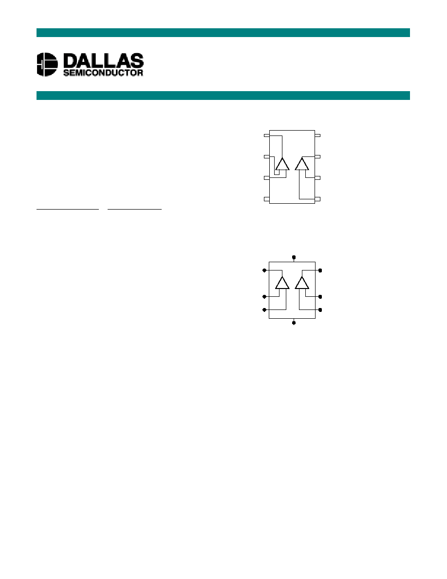
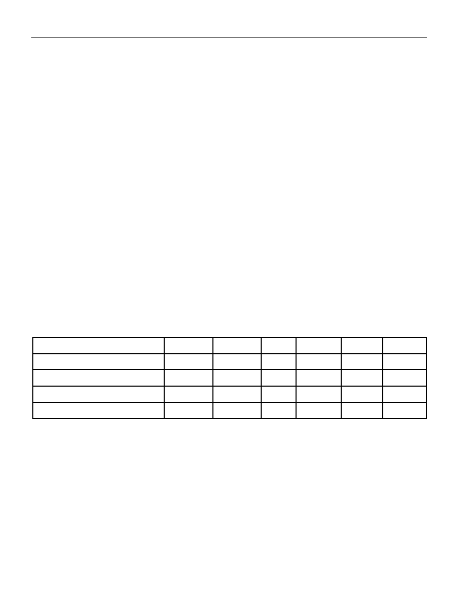
PACKAGES/PINOUTS
A
- +
B
-
+
AOUT
AIN-
AIN+
GND
VDD
BOUT
BIN-
BIN+
1
2
3
4
5
6
7
8
300-mil DIP
150-mil SOIC
118-mil
µ
-SOP
A
- +
B
-
+
AOUT
AIN-
AIN+
GND
VDD
BOUT
BIN-
BIN+
1
2
3
4
5
6
7
8
8-bump CSP
DESCRIPTION
The DS4812 BiCMOS dual operational amplifier combines high slew rate and rail-to-rail output swing.
The device provides 10V/
µ
s of slew rate and 6.5 MHz of bandwidth while only consuming 1.5 mA of
supply current per channel. Ideal low voltage BiFET substitute for low gain, high speed applications.
www.dalsemi.com
DS4812
Low Voltage, High Slew Rate,
Rail-To-Rail Dual Op-Amp
PRELIMINARY
DS4812
2 of 19
ABSOLUTE MAXIMUM RATINGS
Supply Voltage, V
DD
(see Note 1)............5.5V
Differential Input Voltage (see Note 2)....
±
V
DD
Input Voltage Range, V
I
(see Note 1) .......-0.3V to V
DD
Input Current, I
DD
.....................................
±
4 mA
Output Current, I
O
....................................
±
50 mA
Total current into V
DD
..............................
±
50 mA
Total current out of GND.........................
±
50 mA
Duration of short-circuit current (See Note 3) unlimited
Operating Temperature ............................0
o
C to +70
o
C
Storage Temperature ................................-55
o
C to +125
o
C
Soldering Temperature.............................See J-STD-020A Specification
NOTES:
1.
Relative to GND.
2.
Non-inverting input relative to inverting input. Excessive current flows when input is brought below
GND - 0.3V.
3.
The output may be shorted to either supply. Temperature and/or supply voltages must be limited to
ensure that the maximum dissipation rating is not exceeded.
RECOMMENDED OPERATING CONDITIONS
PARAMETER
SYMBOL
MIN
TYP
MAX
UNITS
NOTES
Supply Voltage
V
DD
2.5
5.5
V
1
Input Voltage Range
V
I
0
V
DD
- 1.7
V
1
Common-Mode Input Voltage
V
CM
0
V
DD
- 1.7
V
Free-Air Operating Temperature
T
A
0
70
o
C
NOTES:
1.
Voltage referenced to GND.
DS4812
3 of 19
ELECTRICAL CHARACTERISTICS
Conditions: (T
A
: 0
°
C 70
°
C. V
DD
= 3.0V)
PARAMETER
SYMBOL
MIN
TYP
MAX
UNITS
NOTES
Input Offset Voltage
(V
IC
= 0.5V, R
S
= 50
, V
OUT
= 1.5V)
V
IO
1
5
mV
Temperature Coefficient of Input Offset
Voltage
(V
IC
= 0.5V, R
S
= 50
, V
OUT
= 1.5V)
V
IO
10
µ
V/
°
C
Input Offset Current
(V
IC
= 0.5V, R
S
= 50
, V
OUT
= 1.5V)
I
IO
1
500
pA
Input Bias Current
(V
IC
= 0.5V, R
S
= 50
, V
OUT
= 1.5V)
I
IB
2
500
pA
Common-mode Input Voltage Range
|V
IO
|
10mV
V
ICR
0
1.3
V
High Level Output Voltage
(I
OH
= -0.5 mA)
V
OH
2.5
2.8
V
Low Level Output Voltage
(I
OL
= 0.5 mA)
V
OL
0.15
0.5
V
Large Signal Differential Voltage
Amplification
(V
IC
= 0.5V, R
L
= 10 k
, 1V
V
O
2V)
A
VD
60
68
dB
Common Mode Input Capacitance
c
i(c)
4
pF
Common Mode Rejection Ratio
(0V
V
IC
1.0V, V
O
= 1.5V)
CMRR
40
50
dB
Supply Voltage Rejection Ratio
(3V
V
DD
5V, V
IC
= V
DD
/2 1V, no
load)
k
SVR
70
80
dB
Amplifier Supply Current (per channel)
(V
O
= 1.5V, no load)
I
DD
1.5
2.5
mA
Slew Rate at Unity Gain
(C
L
= 50 pF)
SR
5
7.5
V/
µ
s
Unity Gain Bandwidth
(C
L
= 50 pF)
UGBW
5.0
MHz
Phase Margin at Unity Gain
(C
L
= 50 pF)
M
54
Degree
Gain Margin
(C
L
= 50 pF)
6
dB
DS4812
4 of 19
ELECTRICAL CHARACTERISTICS cont.
Conditions: (T
A
: 0
°
C 70
°
C. V
DD
= 5.0V)
PARAMETER
SYMBOL
MIN
TYP MAX UNITS NOTES
Input Offset Voltage
(V
IC
= 1.5V, R
S
= 50
, V
OUT
= 2.5V)
V
IO
1
5
mV
Temperature Coefficient of Input Offset
Voltage
(V
IC
= 1.5V, R
S
= 50
, V
OUT
= 2.5V)
V
IO
10
µ
V/
°
C
Input Offset Current
(V
IC
= 1.5V, R
S
= 50
, V
OUT
= 2.5V)
I
IO
1
500
pA
Input Bias Current
(V
IC
= 1.5V, R
S
= 50
, V
OUT
= 2.5V)
I
IB
2
500
pA
Common-mode Input Voltage Range
|V
IO
|
10 mV
V
ICR
0
3.3
V
High Level Output Voltage
(I
OH
= -1.0 mA)
V
OH
4.5
4.8
V
Low Level Output Voltage
(I
OL
= 1.0 mA)
V
OL
0.15
0.5
V
Large Signal Differential Voltage
Amplification
(V
IC
= 1.5V, R
L
= 10 k
, 1.5V
V
O
3.5V)
A
VD
60
72
dB
Common Mode Input Capacitance
c
i(c)
4
pF
Common Mode Rejection Ratio
(0V
V
IC
2.7V, V
O
= 2.5V)
CMRR
45
55
dB
Supply Voltage Rejection Ratio
(3V
V
DD
5V, V
IC
= V
DD
/2 1V, no load)
k
SVR
70
80
dB
Amplifier Supply Current (per channel)
(V
O
= 2.5V, no load)
I
DD
1.75
2.5
mA
Slew Rate at Unity Gain
(C
L
= 50 pF)
SR
7
10
V/
µ
s
Unity Gain Bandwidth
(C
L
= 50 pF)
UGBW
6.5
MHz
Phase Margin at Unity Gain
(C
L
= 50 pF)
M
46
Degree
Gain Margin
(C
L
= 50 pF)
4
dB
DS4812
5 of 19
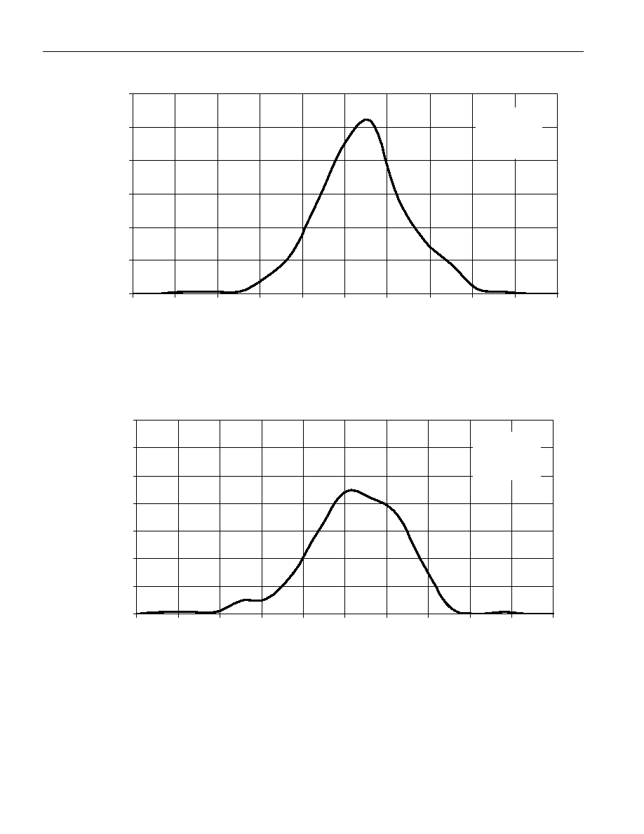
Figure 1.0
Figure 2.0
DISTRIBUTION OF DS4812
INPUT OFFSET VOLTAGE
0%
5%
10%
15%
20%
25%
30%
-2.0
-1.6
-1.2
-0.8
-0.4
0.0
0.4
0.8
1.2
1.6
2.0
V
IO
- Input Offset Voltage - mV
Pe
r
c
e
n
t
a
ge
of
A
m
plif
ie
r
s
-
%
V
DD
= 3.0 V
R
L
= 10K
T
A
= 25
o
C
DISTRIBUTION OF DS4812
INPUT OFFSET VOLTAGE
0%
5%
10%
15%
20%
25%
30%
35%
-2
-1.6
-1.2
-0.8
-0.4
0
0.4
0.8
1.2
1.6
2
V
IO
- Input Offset Voltage - mV
Pe
r
c
e
n
t
a
ge
of
A
m
plif
ie
r
s
-
%
V
DD
= 5.0 V
R
L
= 10K
T
A
= 25
o
C