 | ÐлекÑÑоннÑй компоненÑ: MAX1185 | СкаÑаÑÑ:  PDF PDF  ZIP ZIP |
Äîêóìåíòàöèÿ è îïèñàíèÿ www.docs.chipfind.ru
General Description
The MAX1185 is a +3V, dual 10-bit analog-to-digital
converter (ADC) featuring fully-differential wideband
track-and-hold (T/H) inputs, driving two pipelined,
nine-stage ADCs. The MAX1185 is optimized for low-
power, high dynamic performance applications in
imaging, instrumentation, and digital communication
applications. This ADC operates from a single +2.7V to
+3.6V supply, consuming only 105mW while delivering
a typical signal-to-noise ratio (SNR) of 59.5dB at an
input frequency of 7.5MHz and a sampling rate of
20Msps. Digital outputs A and B are updated alternat-
ing on the rising (CHA) and falling (CHB) edge of the
clock. The T/H driven input stages incorporate 400MHz
(-3dB) input amplifiers. The converters may also be
operated with single-ended inputs. In addition to low
operating power, the MAX1185 features a 2.8mA sleep
mode as well as a 1µA power-down mode to conserve
power during idle periods.
An internal +2.048V precision bandgap reference sets
the full-scale range of the ADC. A flexible reference
structure allows the use of this internal or an externally
derived reference, if desired for applications requiring
increased accuracy or a different input voltage range.
The MAX1185 features parallel, multiplexed, CMOS-
compatible three-state outputs. The digital output for-
mat can be set to two's complement or straight offset
binary through a single control pin. The device provides
for a separate output power supply of +1.7V to +3.6V
for flexible interfacing. The MAX1185 is available in a
7mm x 7mm, 48-pin TQFP package, and is specified
for the extended industrial (-40°C to +85°C) tempera-
ture range.
Pin-compatible, nonmultiplexed. high-speed versions of
the MAX1185 are also available. Please refer to the
MAX1180 data sheet for 105Msps, the MAX1181 data
sheet for 80Msps, the MAX1182 data sheet for 65Msps,
the MAX1183 data sheet for 40Msps, and the MAX1184
data sheet for 20Msps.
Applications
High Resolution Imaging
I/Q Channel Digitization
Multichannel IF Sampling
Instrumentation
Video Application
Ultrasound
Features
o Single +3V Operation
o Excellent Dynamic Performance:
59.5dB SNR at f
IN
= 7.5MHz
74dB SFDR at f
IN
= 7.5MHz
o Low Power:
35mA (Normal Operation)
2.8mA (Sleep Mode)
1µA (Shutdown Mode)
o 0.02dB Gain and 0.25° Phase Matching
o Wide ±1Vp-p Differential Analog Input Voltage
Range
o 400MHz, -3dB Input Bandwidth
o On-Chip +2.048V Precision Bandgap Reference
o Single 10-Bit Bus for Multiplexed, Digital Outputs
o User-Selectable Output Format Two's
Complement or Offset Binary
o 48-Pin TQFP Package with Exposed Paddle For
Improved Thermal Dissipation
MAX1185
Dual 10-Bit, 20Msps, +3V, Low-Power ADC with
Internal Reference and Multiplexed Parallel Outputs
________________________________________________________________ Maxim Integrated Products
1
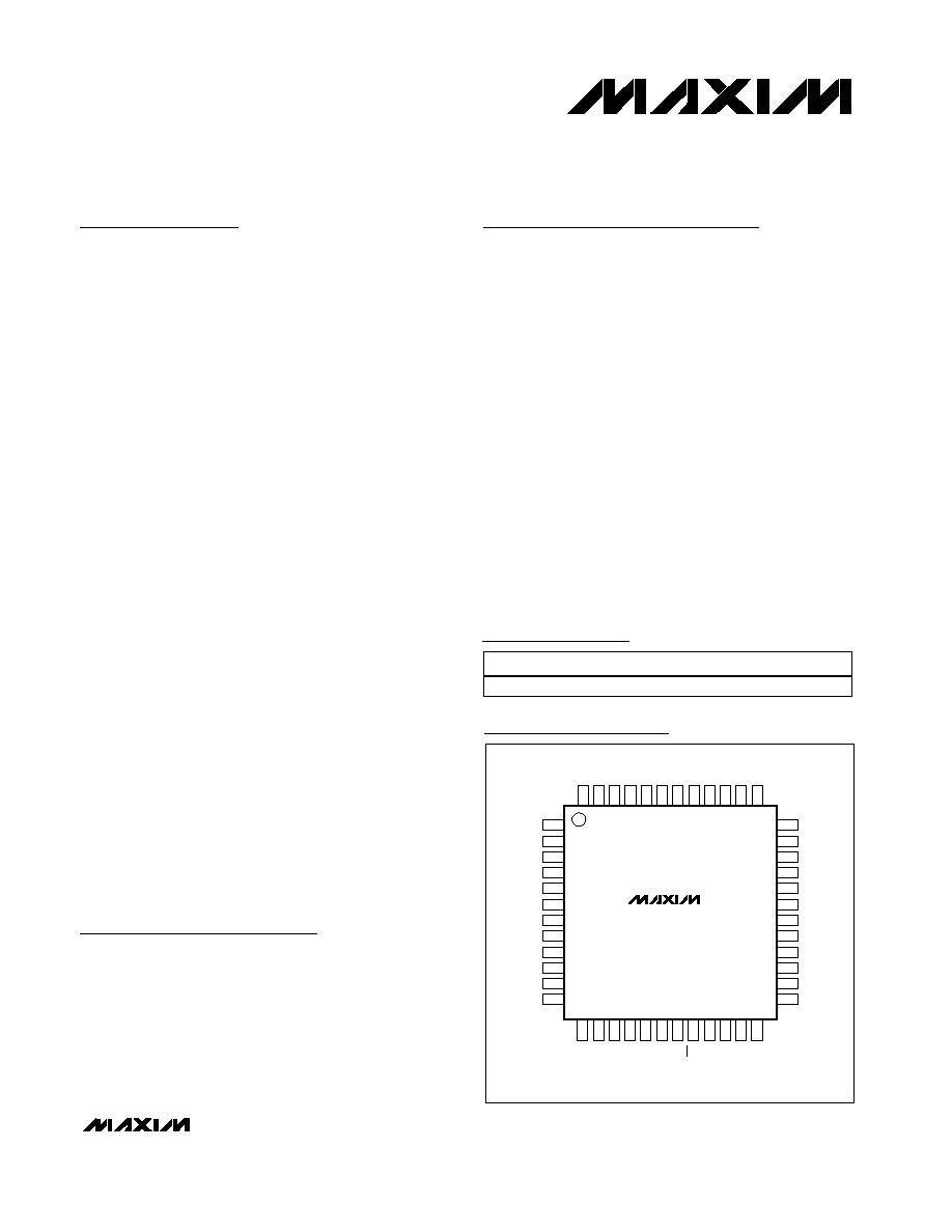
D1A/B
D0A/B
OGND
OV
DD
OV
DD
OGND
A/B
N.C.
N.C.
N.C.
N.C.
N.C.
COM
V
DD
GND
INA+
INA-
V
DD
GND
INB-
INB+
GND
V
DD
CLK
1
2
3
4
5
6
7
8
9
10
11
12
36
35
34
33
32
31
30
29
28
27
26
25
48-TQFP-EP
GND
V
DD
GND
V
DD
T/B
SLEEP
PD
OE
N.C.
N.C.
N.C.
N.C.
13
14
15
16
17
18
19
20
21
22
23
24
48
47
46
45
44
43
42
41
40
39
38
37
REFN
REFP
REFIN
REFOUT
D9A/B
D8A/B
D7A/B
D6A/B
D5A/B
D4A/B
D3A/B
D2A/B
MAX1185
Pin Configuration
19-2175; Rev 0; 10/01
Ordering Information
PART
TEMP. RANGE
PIN-PACKAGE
MAX1185ECM
-40
°C to +85°C
48 TQFP-EP
For pricing, delivery, and ordering information, please contact Maxim/Dallas Direct! at
1-888-629-4642, or visit Maxim's website at www.maxim-ic.com.
MAX1185
Dual 10-Bit, 20Msps, +3V, Low-Power ADC with
Internal Reference and Multiplexed Parallel Outputs
2
_______________________________________________________________________________________
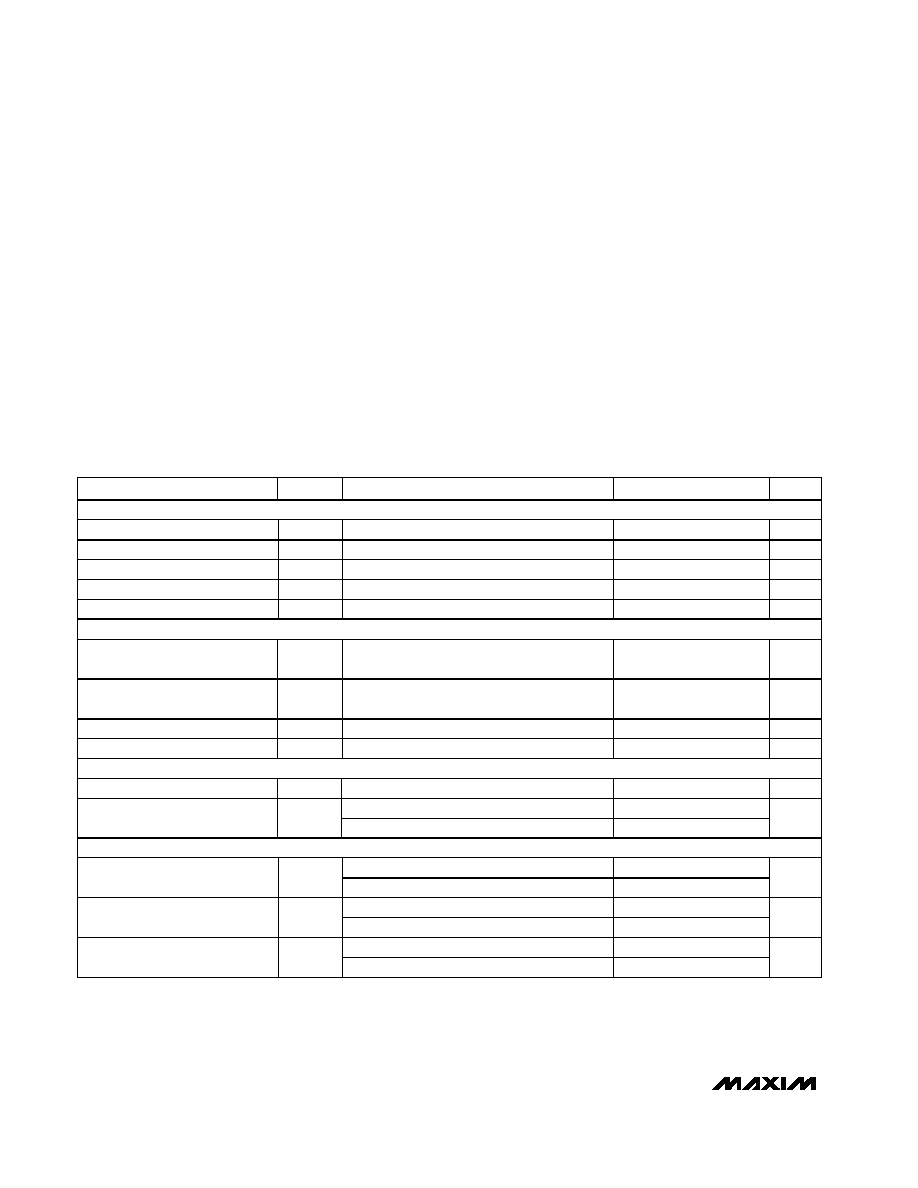
ABSOLUTE MAXIMUM RATINGS
ELECTRICAL CHARACTERISTICS
(V
DD
= +3V, OV
DD
= +2.5V, 0.1µF and 1µF capacitors from REFP, REFN, and COM to GND; REFOUT connected to REFIN through a
10k
resistor, V
IN
= 2Vp-p (differential w.r.t. COM), C
L
= 10pF at digital outputs (Note 5), f
CLK
= 20MHz,
T
A
= T
MIN
to T
MAX
, unless otherwise noted. Typical values are at T
A
= +25°C.)
Stresses beyond those listed under "Absolute Maximum Ratings" may cause permanent damage to the device. These are stress ratings only, and functional
operation of the device at these or any other conditions beyond those indicated in the operational sections of the specifications is not implied. Exposure to
absolute maximum rating conditions for extended periods may affect device reliability.
V
DD
, OV
DD
to GND ...............................................-0.3V to +3.6V
OGND to GND.......................................................-0.3V to +0.3V
INA+, INA-, INB+, INB- to GND ...............................-0.3V to V
DD
REFIN, REFOUT, REFP, REFN, COM,
CLK to GND............................................-0.3V to (V
DD
+ 0.3V)
OE, PD, SLEEP, T/B, D9A/BD0A/B,
A/B to OGND .......................................-0.3V to (OV
DD
+ 0.3V)
Continuous Power Dissipation (T
A
= +70°C)
48-Pin TQFP (derate 12.5mW/°C above +70°C).......1000mW
Operating Temperature Range ...........................-40°C to +85°C
Junction Temperature ......................................................+150°C
Storage Temperature Range .............................-60°C to +150°C
Lead Temperature (soldering, 10s) .................................+300°C
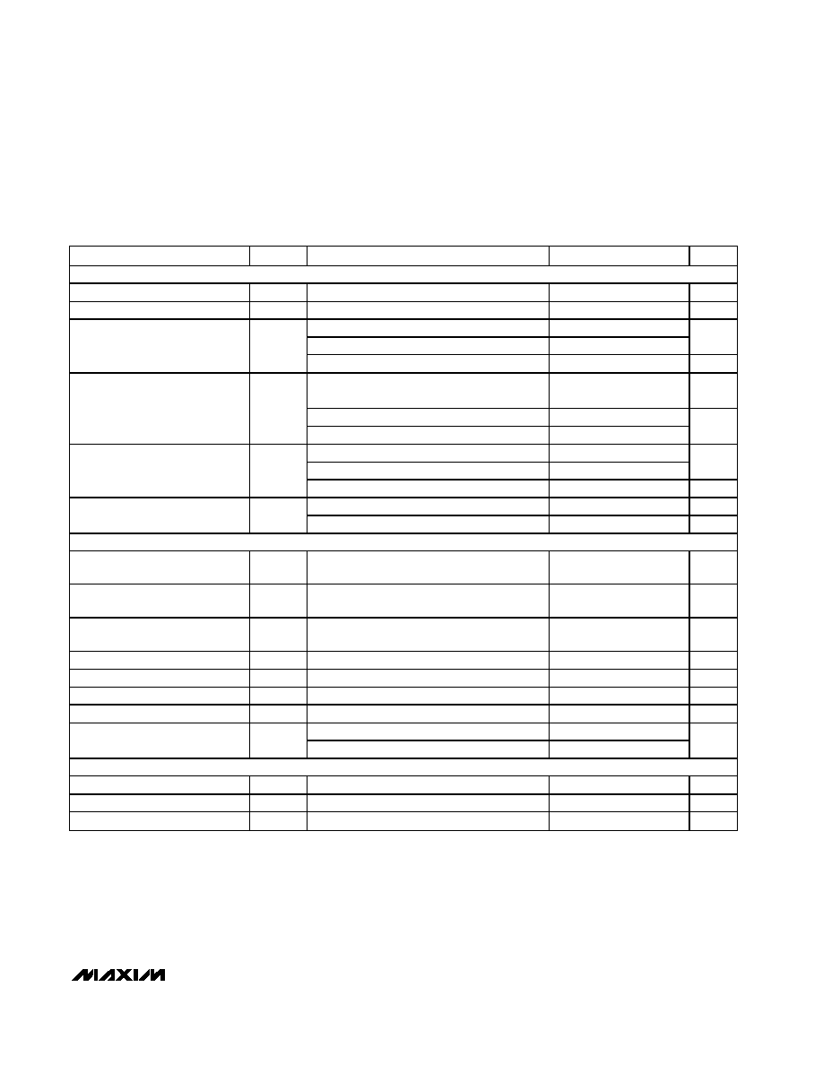
PARAMETER
SYMBOL
CONDITIONS
MIN
TYP
MAX
UNITS
DC ACCURACY
Resolution
10
Bits
Integral Nonlinearity
INL
f
IN
= 7.5MHz
±0.5
±1.5
LSB
Differential Nonlinearity
DNL
f
IN
= 7.5MHz, no missing codes guaranteed
±0.25
±1.0
LSB
Offset Error
<
±1
±1.7
% FS
Gain Error
0
±2
% FS
ANALOG INPUT
Differential Input Voltage
Range
V
DIFF
Differential or single-ended inputs
±1.0
V
Common-Mode Input Voltage
Range
V
CM
V
DD
/2
± 0.5
V
Input Resistance
R
IN
Switched capacitor load
100
k
Input Capacitance
C
IN
5
pF
CONVERSION RATE
Maximum Clock Frequency
f
CLK
20
MHz
CHA
5
Data Latency
CHB
5.5
Clock
Cycles
DYNAMIC CHARACTERISTICS (f
CLK
= 20MHz, 4096-point FFT)
f
INA or B
= 7.5MHz, T
A
= +25
°C
57.3
59.5
Signal-to-Noise Ratio
SNR
f
INA or B
= 12MHz
59.4
dB
f
INA or B
= 7.5MHz, T
A
= +25
°C
57
59.4
Signal-to-Noise and Distortion
SINAD
f
INA or B
= 12MHz
59.2
dB
f
INA or B
= 7.5MHz, T
A
= +25
°C
64
74
Spurious-Free Dynamic Range
SFDR
f
INA or B
= 12MHz
72
dBc
MAX1185
Dual 10-Bit, 20Msps, +3V, Low-Power ADC with
Internal Reference and Multiplexed Parallel Outputs
_______________________________________________________________________________________
3
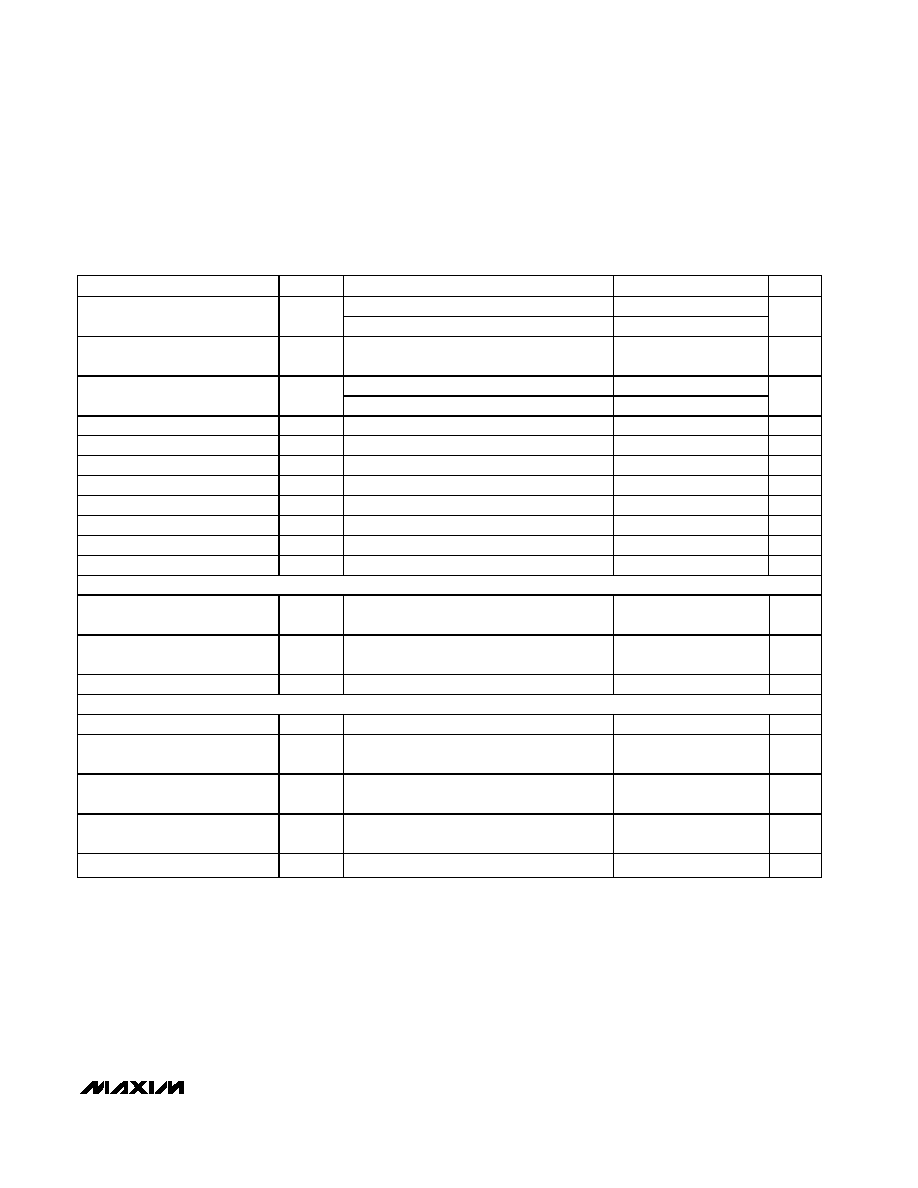
ELECTRICAL CHARACTERISTICS (continued)
(V
DD
= +3V, OV
DD
= +2.5V, 0.1µF and 1µF capacitors from REFP, REFN, and COM to GND; REFOUT connected to REFIN through a
10k
resistor, V
IN
= 2Vp-p (differential w.r.t. COM), C
L
= 10pF at digital outputs (Note 5), f
CLK
= 20MHz,
T
A
= T
MIN
to T
MAX
, unless otherwise noted. Typical values are at T
A
= +25°C.)
PARAMETER
SYMBOL
CONDITIONS
MIN
TYP
MAX
UNITS
f
INA or B
= 7.5MHz
-74
Third-Harmonic Distortion
HD3
f
INA or B
= 12MHz
-72
dBc
f
INA or B
= 11.9852MHz at -6.5dB FS
Intermodulation Distortion
IMD
f
I N A o r B
= 12.8934M H z at - 6.5d B FS ( N ote 2)
-76
dBc
f
INA or B
= 7.5MHz, T
A
= +25
°C
-72
-64
Total Harmonic Distortion
(first 4 harmonics)
THD
f
INA or B
= 12MHz
-71
dBc
Small-Signal Bandwidth
Input at -20dB FS, differential inputs
500
MHz
Full-Power Bandwidth
FPBW
Input at -0.5dB FS, differential inputs
400
MHz
Aperture Delay
t
AD
1
ns
Aperture Jitter
t
AJ
2
ps
RMS
Overdrive Recovery Time
For 1.5
full-scale input
2
ns
Differential Gain
±1
%
Differential Phase
±0.25
d egr ees
Output Noise
INA+ = INA- = INB+ = INB- = COM
0.2
LSB
RMS
INTERNAL REFERENCE
Reference Output Voltage
REFOUT
2.048
±3%
V
Reference Temperature
Coefficient
TC
REF
60
ppm/°C
Load Regulation
1.25
mV/mA
BUFFERED EXTERNAL REFERENCE (V
REFIN
= +2.048V)
REFIN Input Voltage
V
REFIN
2.048
V
Positive Reference Output
Voltage
V
REFP
2.012
V
Negative Reference Output
Voltage
V
REFN
0.988
V
Differential Reference Output
Voltage Range
VREF
VREF = VREFP - VREFN
0.98
1.024
1.07
V
REFIN Resistance
R
REFIN
>50
M
MAX1185
Dual 10-Bit, 20Msps, +3V, Low-Power ADC with
Internal Reference and Multiplexed Parallel Outputs
4
_______________________________________________________________________________________
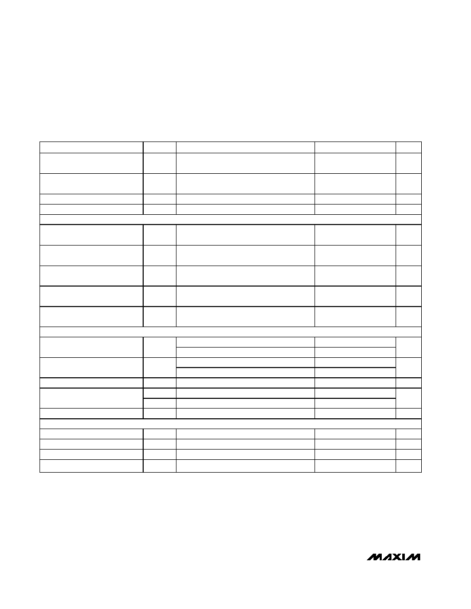
ELECTRICAL CHARACTERISTICS (continued)
(V
DD
= +3V, OV
DD
= +2.5V, 0.1µF and 1µF capacitors from REFP, REFN, and COM to GND; REFOUT connected to REFIN through a
10k
resistor, V
IN
= 2Vp-p (differential w.r.t. COM), C
L
= 10pF at digital outputs (Note 5), f
CLK
= 20MHz,
T
A
= T
MIN
to T
MAX
, unless otherwise noted. Typical values are at T
A
= +25°C.)
PARAMETER
SYMBOL
CONDITIONS
MIN
TYP
MAX
UNITS
Maximum REFP, COM Source
Current
I
SOURCE
5
mA
Maximum REFP, COM Sink
Current
I
SINK
-250
µA
Maximum REFN Source Current
I
SOURCE
250
µA
Maximum REFN Sink Current
I
SINK
-5
mA
UNBUFFERED EXTERNAL REFERENCE (V
REFIN
= AGND, reference voltage applied to REFP, REFN, and COM)
REFP, REFN Input Resistance
R
REFP
,
R
REFN
Measured between REFP and COM, and
REFN and COM
4
k
Differential Reference Input
Voltage
V
REF
V
REF
= V
REFP
- V
REFN
1.024
±10%
V
COM Input Voltage
V
COM
V
DD
/2
±10%
V
REFP Input Voltage
V
REFP
V
COM
+
V
REF
/2
V
REFN Input Voltage
V
REFN
V
COM
-
V
REF
/2
V
DIGITAL INPUTS (CLK, PD, OE, SLEEP, T/B)
CLK
0.8
V
DD
Input High Threshold
V
IH
PD, OE, SLEEP, T/B
0.8
OV
DD
V
CLK
0.2
V
DD
Input Low Threshold
V
IL
PD, OE, SLEEP, T/B
0.2
OV
DD
V
Input Hysteresis
V
HYST
0.1
V
I
IH
V
IH
= OV
DD
or V
DD
(CLK)
±5
Input Leakage
I
IL
V
IL
= 0
±5
µA
Input Capacitance
C
IN
5
pF
DIGITAL OUTPUTS (D0A/BD9A/B, A/B)
Output Voltage Low
V
OL
I
SINK
= -200µA
0.2
V
Output Voltage High
V
OH
I
SOURCE
= 200µA
OV
DD
- 0.2
V
Three-State Leakage Current
I
LEAK
OE = OV
DD
±10
µA
Three-State Output Capacitance
C
OUT
OE = OV
DD
5
pF
MAX1185
Dual 10-Bit, 20Msps, +3V, Low-Power ADC with
Internal Reference and Multiplexed Parallel Outputs
_______________________________________________________________________________________
5
ELECTRICAL CHARACTERISTICS (continued)
(V
DD
= +3V, OV
DD
= +2.5V, 0.1µF and 1.0µF capacitors from REFP, REFN, and COM to GND; REFOUT connected to REFIN through
a 10k
resistor, V
IN
= 2Vp-p (differential w.r.t. COM), C
L
= 10pF at digital outputs (Note 5), f
CLK
= 20MHz,
T
A
= T
MIN
to T
MAX
, unless otherwise noted. Typical values are at T
A
= +25°C.)
PARAMETER
SYMBOL
CONDITIONS
MIN
TYP
MAX
UNITS
POWER REQUIREMENTS
Analog Supply Voltage Range
V
DD
2.7
3.0
3.6
V
Output Supply Voltage Range
OV
DD
1.7
2.5
3.6
V
Operating, f
INA or B
= 7.5MHz at -0.5dB FS
35
50
Sleep mode
2.8
mA
Analog Supply Current
I
VDD
Shutdown, clock idle, PD = OE = OV
DD
1
15
µA
Operating, C
L
= 15pF, f
INA or B
= 7.5MHz at
-0.5dB FS
4
mA
Sleep mode
100
Output Supply Current
I
OVDD
Shutdown, clock idle, PD = OE = OV
DD
2
10
µA
Operating, f
INA or B
= 7.5MHz at -0.5dB FS
105
150
Sleep mode
8.4
mW
Power Dissipation
PDISS
Shutdown, clock idle, PD = OE = OV
DD
3
45
µW
Offset
±0.2
mV/V
Power-Supply Rejection Ratio
PSRR
Gain
±0.1
%/V
TIMING CHARACTERISTICS
CLK Rise to CHA Output Data
Valid
t
DOA
Figure 3 (Note 3)
5
8
ns
CLK Fall to CHB Output Data
Valid
t
DOB
Figure 3 (Note 3)
5
8
ns
Clock Rise/Fall to A/B Rise/Fall
Time
t
DA/B
6
ns
Output Enable Time
t
ENABLE
Figure 4
10
ns
Output Disable Time
t
DISABLE
Figure 4
1.5
ns
CLK Pulse Width High
t
CH
Figure 3, clock period: 50ns
25
± 7.5
ns
CLK Pulse Width Low
t
CL
Figure 3, clock period: 50ns
25
± 7.5
ns
Wakeup from sleep mode (Note 4)
0.51
Wake-Up Time
t
WAKE
Wakeup from shutdown (Note 4)
1.5
µs
CHANNEL-TO-CHANNEL MATCHING
Crosstalk
f
INA or B
= 7.5MHz at -0.5dB FS
-70
dB
Gain Matching
f
INA or B
= 7.5MHz at -0.5dB FS
0.02
±0.2
dB
Phase Matching
f
INA or B
= 7.5MHz at -0.5dB FS
0.25
d eg r ees
Note 1: SNR, SINAD, THD, SFDR, and HD3 are based on an analog input voltage of -0.5dB FS referenced to a +1.024V full-scale
input voltage range.
Note 2: Intermodulation distortion is the total power of the intermodulation products relative to the individual carrier. This number is
6dB or better, if referenced to the two-tone envelope.
Note 3: Digital outputs settle to V
IH
, V
IL
. Parameter guaranteed by design.
Note 4: With REFIN driven externally, REFP, COM, and REFN are left floating while powered down.
Note 5: Equivalent dynamic performance is obtainable over full OV
DD
range with reduced C
L
.