 | ÐлекÑÑоннÑй компоненÑ: MAX1208 | СкаÑаÑÑ:  PDF PDF  ZIP ZIP |
Äîêóìåíòàöèÿ è îïèñàíèÿ www.docs.chipfind.ru
General Description
The MAX1206 is a 3.3V, 12-bit analog-to-digital converter
(ADC) featuring a fully differential wideband track-and-
hold (T/H) input, driving the internal quantizer. The
MAX1206 is optimized for low power, small size, and
high dynamic performance. This ADC operates from a
single 3.0V to 3.6V supply, consuming only 159mW,
while delivering a typical signal-to-noise ratio (SNR) per-
formance of 68.6dB at a 20MHz input frequency. The
T/H-driven input stage accepts single-ended or differen-
tial inputs. In addition to low operating power, the
MAX1206 features a 0.15mW power-down mode to con-
serve power during idle periods.
A flexible reference structure allows the MAX1206 to
use its internal precision bandgap reference or accept
an externally applied reference. A common-mode refer-
ence is provided to simplify design and reduce external
component count in differential analog input circuits.
The MAX1206 supports both a single-ended and differ-
ential input clock drive. Wide variations in the clock
duty cycle are compensated with the ADC's internal
duty-cycle equalizer.
The MAX1206 features parallel, CMOS-compatible out-
puts. The digital output format is pin selectable to be
either two's complement or Gray code. A data-valid indi-
cator eliminates external components that are normally
required for reliable digital interfacing. A separate power
input for the digital outputs accepts a voltage from 1.7V
to 3.6V for flexible interfacing with various logic levels.
The MAX1206 is available in a 6mm x 6mm x 0.8mm, 40-
pin thin QFN package with exposed paddle (EP), and is
specified for the extended industrial (-40°C to +85°C)
temperature range.
Refer to the MAX1209 and MAX1211 (see Pin-Compatible
Higher/Speed Versions table) for applications that require
high dynamic performance for IF input frequencies.
Applications
Communication Receivers
Cellular, LMDS, Point-to-Point Microwave,
MMDS, HFC, WLAN
Ultrasound and Medical Imaging
Portable Instrumentation
Low-Power Data Acquisition
Features
o Excellent Dynamic Performance
68.6dB SNR at f
IN
= 20MHz
90dBc SFDR at f
IN
= 20MHz
o Low-Power Operation
159mW at 3.0V (Single-Ended Clock)
181mW at 3.3V (Single-Ended Clock)
198mW at 3.3V (Differential Clock)
o Differential or Single-Ended Clock
o Accepts 20% to 80% Clock Duty Cycle
o Fully Differential or Single-Ended Analog Input
o Adjustable Full-Scale Analog Input Range
o Common-Mode Reference
o Power-Down Mode
o CMOS-Compatible Outputs in Two's Complement
or Gray Code
o Data-Valid Indicator Simplifies Digital Design
o Out-of-Range and Data-Valid Indicators
o Miniature, 40-Pin Thin QFN Package with Exposed
Paddle
o Pin-Compatible, IF Sampling ADC Available
(MAX1211ETL)
o Evaluation Kit Available (Order MAX1211EVKIT)
MAX1206
40Msps, 12-Bit ADC
________________________________________________________________ Maxim Integrated Products
1
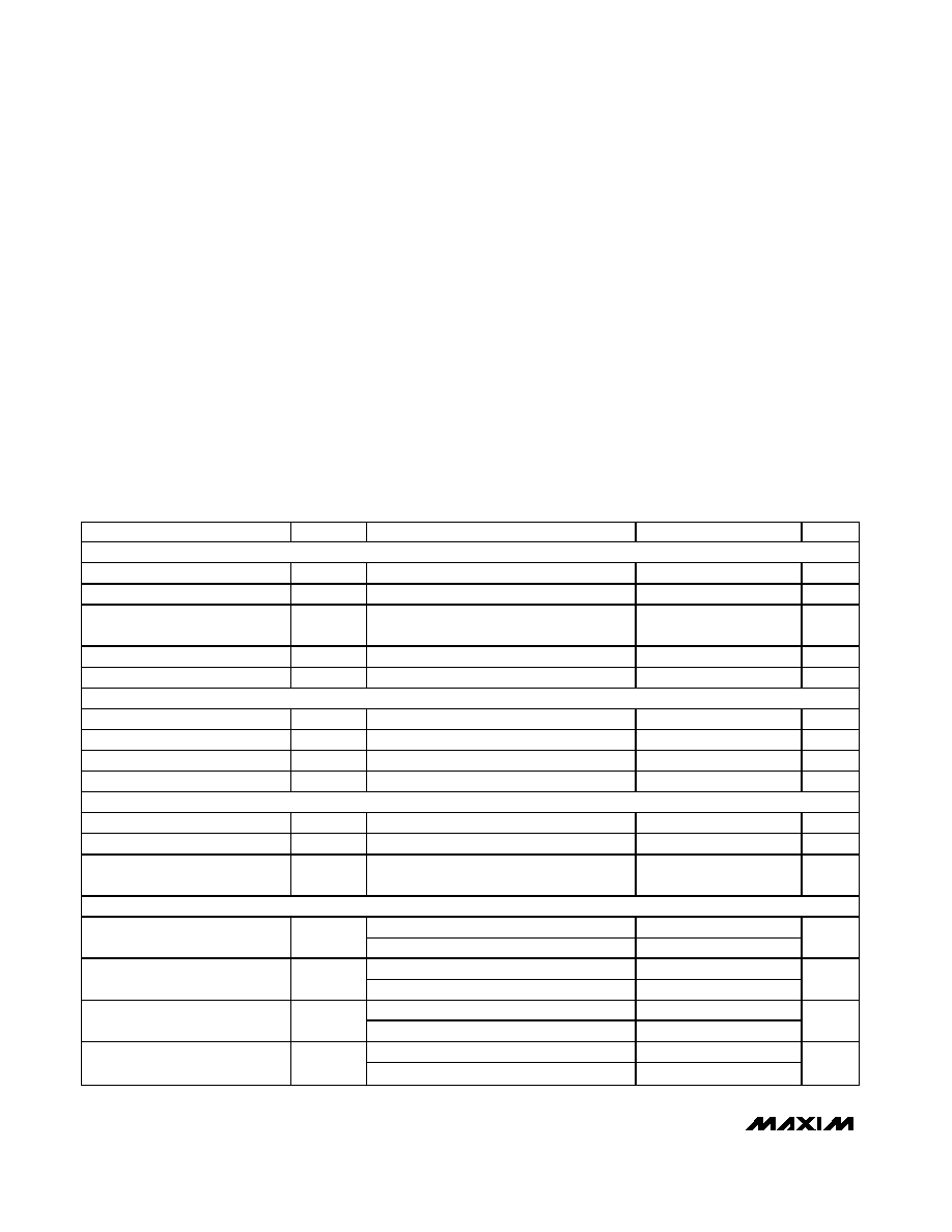
Ordering Information
19-3259; Rev 0; 5/04
For pricing, delivery, and ordering information, please contact Maxim/Dallas Direct! at
1-888-629-4642, or visit Maxim's website at www.maxim-ic.com.
EVALUATION KIT
AVAILABLE
PART
TEMP RANGE
PIN-PACKAGE
MAX1206ETL
-40°C to +85°C
40 Thin QFN (6mm x 6mm)
Pin-Compatible Higher
Speed Versions
PART
SPEED GRADE
(Msps)
TARGET
APPLICATION
MAX1206
40
Baseband
MAX1207
65
Baseband
MAX1208
80
Baseband
MAX1211
65
IF
MAX1209
80
IF
Pin Configuration appears at end of data sheet.
MAX1206
40Msps, 12-Bit ADC
2
_______________________________________________________________________________________
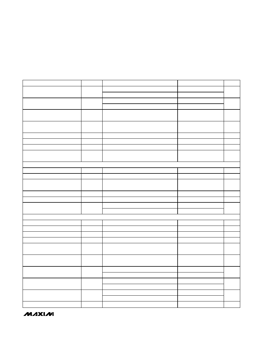
ABSOLUTE MAXIMUM RATINGS
Stresses beyond those listed under "Absolute Maximum Ratings" may cause permanent damage to the device. These are stress ratings only, and functional
operation of the device at these or any other conditions beyond those indicated in the operational sections of the specifications is not implied. Exposure to
absolute maximum rating conditions for extended periods may affect device reliability.
V
DD
to GND ...........................................................-0.3V to +3.6V
OV
DD
to GND........-0.3V to the lower of (V
DD
+ 0.3V) and +3.6V
INP, INN to GND ...-0.3V to the lower of (V
DD
+ 0.3V) and +3.6V
REFIN, REFOUT, REFP, REFN,
COM to GND.....-0.3V to the lower of (V
DD
+ 0.3V) and +3.6V
CLKP, CLKN, CLKTYP, G/T, DCE,
PD to GND ........-0.3V to the lower of (V
DD
+ 0.3V) and +3.6V
D11D0, I.C., DAV, DOR to GND ............-0.3V to (OV
DD
+ 0.3V)
Continuous Power Dissipation (T
A
= +70°C)
40-Pin Thin QFN 6mm x 6mm x 0.8mm
(derated 26.3mW/°C above +70°C)........................2105.3mW
Operating Temperature Range ...........................-40°C to +85°C
Junction Temperature ......................................................+150°C
Storage Temperature Range .............................-65°C to +150°C
Lead Temperature (soldering 10s) ..................................+300°C
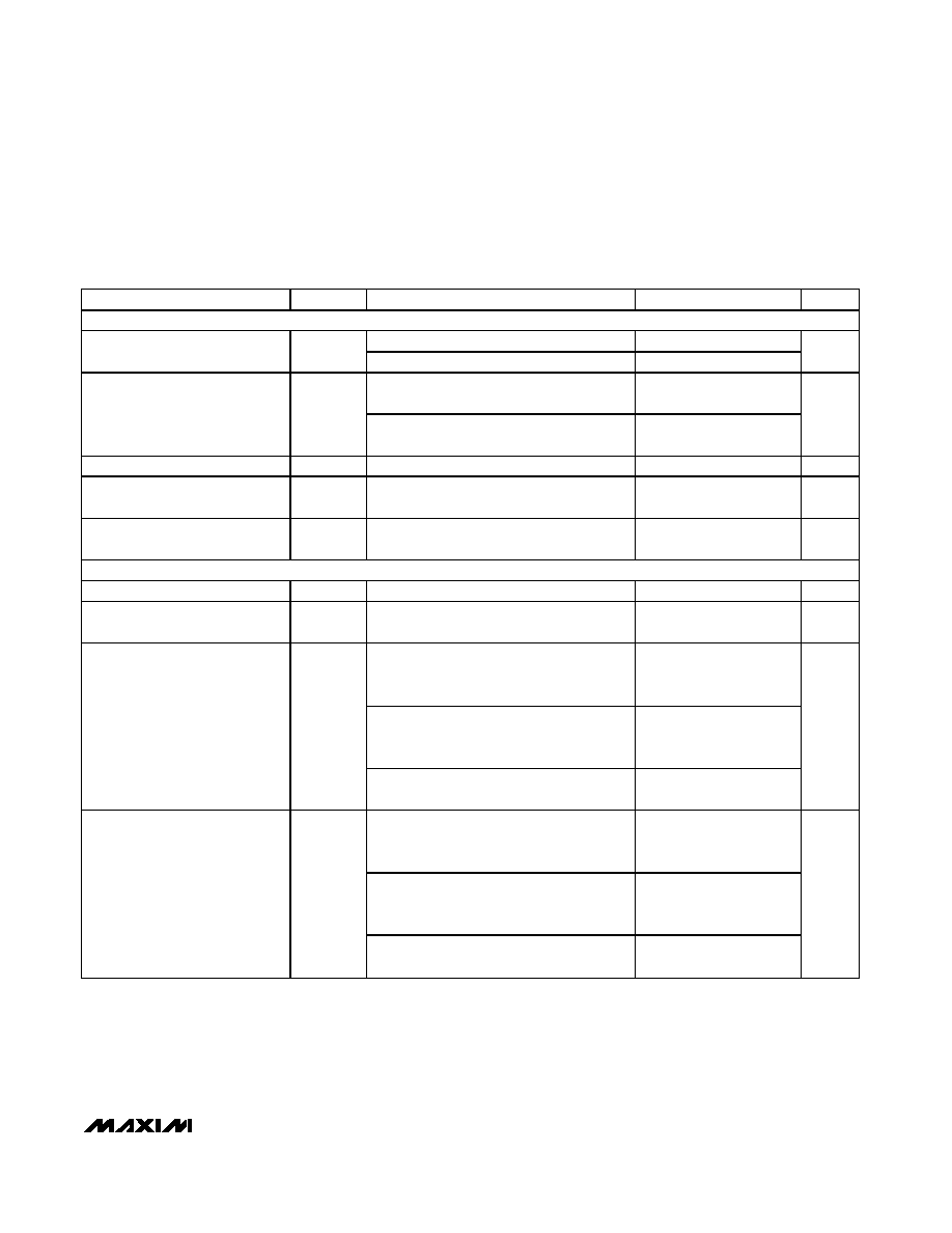
ELECTRICAL CHARACTERISTICS
(V
DD
= 3.3V, OV
DD
= 2.0V, GND = 0, REFIN = REFOUT (internal reference), C
REFOUT
= 0.1µF, C
L
5pF at digital outputs, V
IN
=
-0.5dBFS, CLKTYP = high, DCE = high, PD = low, G/T = low, f
CLK
= 40MHz (50% duty cycle), C
REFP
= C
REFN
= 0.1µF to GND, 1µF
in parallel with 10µF between REFP and REFN, C
COM
= 0.1µF in parallel with 2.2µF to GND, T
A
= -40°C to +85°C, unless otherwise
noted. Typical values are at T
A
= +25°C.) (Note 1)
PARAMETER
SYMBOL
CONDITIONS
MIN
TYP
MAX
UNITS
DC ACCURACY
Resolution
12
Bits
Integral Nonlinearity
INL
f
IN
= 20MHz (Note 2)
±0.3
±0.7
LSB
Differential Nonlinearity
DNL
f
IN
= 20MHz, no missing codes over
temperature (Note 2)
±0.3
±0.7
LSB
Offset Error
V
REFIN
= 2.048V
±0.2
±1.1
%FS
Gain Error
V
REFIN
= 2.048V
±0.3
±4.8
%FS
ANALOG INPUT (INP, INN)
Differential Input Voltage Range
V
DIFF
Differential or single-ended inputs
±1.024
V
Common-Mode Input Voltage
V
DD
/ 2
V
Input Resistance
R
IN
Switched capacitor load
24
k
Input Capacitance
C
IN
4
pF
CONVERSION RATE
Maximum Clock Frequency
f
CLK
40
MHz
Minimum Clock Frequency
5
MHz
Data Latency
Figure 5
8.5
Clock
cycles
DYNAMIC CHARACTERISTICS (Differential inputs, 4096-point FFT)
f
IN
= 3MHz at -0.5dBFS
68.4
Signal-to-Noise Ratio
SNR
f
IN
= 20MHz at -0.5dBFS (Note 2)
67.0
68.6
dB
f
IN
= 3MHz at -0.5dBFS
68.3
Signal-to-Noise and Distortion
SINAD
f
IN
= 20MHz at -0.5dBFS (Note 2)
66.9
68.5
dB
f
IN
= 3MHz at -0.5dBFS
89.5
Single-Tone Spurious-Free
Dynamic Range
SFDR
f
IN
= 20MHz at -0.5dBFS (Note 2)
83.2
90
dBc
f
IN
= 3MHz at -0.5dBFS
-88.4
Total Harmonic Distortion
THD
f
IN
= 20MHz at -0.5dBFS (Note 2)
-88.4
-81
dBc
MAX1206
40Msps, 12-Bit ADC
_______________________________________________________________________________________
3
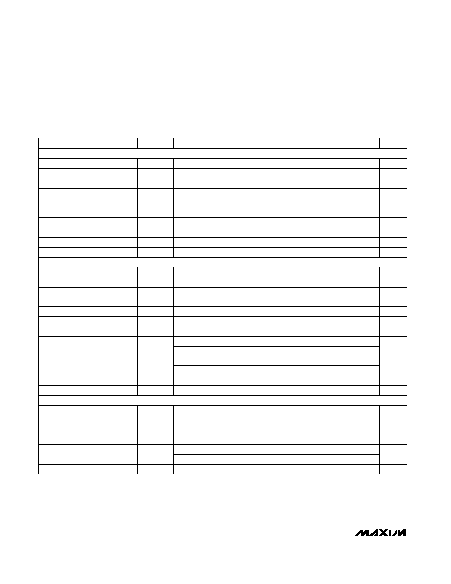
ELECTRICAL CHARACTERISTICS (continued)
(V
DD
= 3.3V, OV
DD
= 2.0V, GND = 0, REFIN = REFOUT (internal reference), C
REFOUT
= 0.1µF, C
L
5pF at digital outputs, V
IN
=
-0.5dBFS, CLKTYP = high, DCE = high, PD = low, G/T = low, f
CLK
= 40MHz (50% duty cycle), C
REFP
= C
REFN
= 0.1µF to GND, 1µF
in parallel with 10µF between REFP and REFN, C
COM
= 0.1µF in parallel with 2.2µF to GND, T
A
= -40°C to +85°C, unless otherwise
noted. Typical values are at T
A
= +25°C.) (Note 1)
PARAMETER
SYMBOL
CONDITIONS
MIN
TYP
MAX
UNITS
f
IN
= 3MHz at -0.5dBFS
-92.5
Second Harmonic
HD2
f
IN
= 20MHz at -0.5dBFS (Note 3)
-96.3
-84.9
dBc
f
IN
= 3MHz at -0.5dBFS
-93.8
Third Harmonic
HD3
f
IN
= 20MHz at -0.5dBFS (Note 3)
-92.1
-83.3
dBc
Third-Order Intermodulation
IM3
f
IN1
= 69MHz at -7dBFS,
f
IN2
= 71MHz at -7dBFS
-89
dBc
Two-Tone Spurious-Free
Dynamic Range
SFDR
TT
f
IN1
= 69MHz at -7dBFS,
f
IN2
= 71MHz at -7dBFS
88
dBc
Aperture Delay
t
AD
Figure 14
0.9
ns
Aperture Jitter
t
AJ
Figure 14
<0.2
ps
RMS
Output Noise
n
OUT
INP = INN = COM
0.5
LSB
RMS
Overdrive Recovery Time
±10% beyond full scale
1
Clock
cycles
INTERNAL REFERENCE (REFIN = REFOUT; V
REFP
, V
REFN
, and V
COM
are generated internally)
REFOUT Output Voltage
V
REFOUT
1.988
2.048
2.080
V
COM Output Voltage
V
COM
V
DD
/ 2
1.65
V
Differential Reference Output
Voltage
V
REF
V
REF
= V
REFP
- V
REFN
1.024
V
REFOUT Load Regulation
35
mV/mA
REFOUT Temperature Coefficient
TC
REF
+100
ppm/°C
Short to V
DD
0.24
REFOUT Short-Circuit Current
Short to GND
2.1
mA
B U F F ER ED EXT ER N A L R EF ER EN C E ( RE FIN d r i ven exter nal l y, V
R E F IN
= 2.048V , V
R E F P
, V
R E F N
, and V
C OM
ar e g ener ated i nter nal l y)
REFIN Input Voltage
V
REFIN
2.048
V
REFP Output Voltage
V
REFP
(V
DD
/ 2) + (V
REFIN
/ 4)
2.162
V
REFN Output Voltage
V
REFN
(V
DD
/ 2) - (V
REFIN
/ 4)
1.138
V
COM Output Voltage
V
COM
V
DD
/ 2
1.60
1.65
1.70
V
Differential Reference Output
Voltage
V
REF
V
REF
= V
REFP
- V
REFN
0.970
1.024
1.070
V
Differential Reference
Temperature Coefficient
+12.5
ppm/°C
Source
0.4
Maximum REFP Current
I
REFP
Sink
1.4
mA
Source
1.0
Maximum REFN Current
I
REFN
Sink
1.0
mA
Source
1.0
Maximum COM Current
I
COM
Sink
0.4
mA
REFIN Input Resistance
>50
M
MAX1206
40Msps, 12-Bit ADC
4
_______________________________________________________________________________________
ELECTRICAL CHARACTERISTICS (continued)
(V
DD
= 3.3V, OV
DD
= 2.0V, GND = 0, REFIN = REFOUT (internal reference), C
REFOUT
= 0.1µF, C
L
5pF at digital outputs, V
IN
=
-0.5dBFS, CLKTYP = high, DCE = high, PD = low, G/T = low, f
CLK
= 40MHz (50% duty cycle), C
REFP
= C
REFN
= 0.1µF to GND, 1µF
in parallel with 10µF between REFP and REFN, C
COM
= 0.1µF in parallel with 2.2µF to GND, T
A
= -40°C to +85°C, unless otherwise
noted. Typical values are at T
A
= +25°C.) (Note 1)
PARAMETER
SYMBOL
CONDITIONS
MIN
TYP
MAX
UNITS
UNBUFFERED EXTERNAL REFERENCE (REFIN = GND, V
REFP
, V
REFN
, and V
COM
are applied externally)
COM Input Voltage
V
COM
V
DD
/ 2
1.65
V
REFP Input Voltage
V
REFP
- V
COM
0.512
V
REFN Input Voltage
V
REFN
- V
COM
-0.512
V
Differential Reference Input
Voltage
V
REF
V
REF
= V
REFP
- V
REFN
1.024
V
REFP Sink Current
I
REFP
V
REFP
= 2.162V
1.1
mA
REFN Source Current
I
REFN
V
REFN
= 1.138V
1.1
mA
COM Sink Current
I
COM
0.3
mA
REFP, REFN, Capacitance
13
pF
COM Capacitance
6
pF
CLOCK INPUTS (CLKP, CLKN)
Single-Ended Input High
Threshold
V
IH
CLKTYP = GND, CLKN = GND
0.8 x
V
DD
V
Single-Ended Input Low
Threshold
V
IL
CLKTYP = GND, CLKN = GND
0.2 x
V
DD
V
Differential Input Voltage Swing
CLKTYP = high
1.4
V
P-P
Differential Input Common-Mode
Voltage
CLKTYP = high
V
DD
/ 2
V
DCE = OV
DD
20
Minimum Clock Duty Cycle
DCE = GND
45
%
DCE = OV
DD
80
Maximum Clock Duty Cycle
DCE = GND
60
%
Input Resistance
R
CLK
Figure 4
5
k
Input Capacitance
C
CLK
2
pF
DIGITAL INPUTS (CLKTYP, G/T, PD)
Input High Threshold
V
IH
0.8 x
OV
DD
V
Input Low Threshold
V
IL
0.2 x
OV
DD
V
V
IH
= OV
DD
±5
Input Leakage Current
V
IL
= 0
±5
µA
Input Capacitance
C
DIN
5
pF
MAX1206
40Msps, 12-Bit ADC
_______________________________________________________________________________________
5
ELECTRICAL CHARACTERISTICS (continued)
(V
DD
= 3.3V, OV
DD
= 2.0V, GND = 0, REFIN = REFOUT (internal reference), C
REFOUT
= 0.1µF, C
L
5pF at digital outputs, V
IN
=
-0.5dBFS, CLKTYP = high, DCE = high, PD = low, G/T = low, f
CLK
= 40MHz (50% duty cycle), C
REFP
= C
REFN
= 0.1µF to GND, 1µF
in parallel with 10µF between REFP and REFN, C
COM
= 0.1µF in parallel with 2.2µF to GND, T
A
= -40°C to +85°C, unless otherwise
noted. Typical values are at T
A
= +25°C.) (Note 1)
PARAMETER
SYMBOL
CONDITIONS
MIN
TYP
MAX
UNITS
DIGITAL OUTPUTS (D0D11, DAV, DOR)
D0D11, DOR, I
SINK
= 200µA
0.2
Output-Voltage Low
V
OL
DAV, I
SINK
= 600µA
0.2
V
D0D11, DOR, I
SOURCE
= 200µA
OV
DD
- 0.2
Output-Voltage High
V
OH
DAV, I
SOURCE
= 600µA
OV
DD
- 0.2
V
Tri-State Leakage Current
I
LEAK
(Note 4)
±5
µA
D11D0, DOR Tri-State Output
Capacitance
C
OUT
(Note 4)
3
pF
DAV Tri-State Output
Capacitance
C
DAV
(Note 4)
6
pF
POWER REQUIREMENTS
Analog Supply Voltage
V
DD
3.0
3.3
3.6
V
Digital Output Supply Voltage
OV
DD
1.7
2.0
V
DD
+ 0.3V
V
Normal operating mode,
f
IN
= 20MHz at -0.5dBFS,
CLKTYP = GND, single-ended clock
54.7
Normal operating mode,
f
IN
= 20MHz at -0.5dBFS,
CLKTYP = OV
DD
, differential clock
60.1
66
Analog Supply Current
I
VDD
Power-down mode; clock idle,
PD = OV
DD
0.045
mA
Normal operating mode,
f
IN
= 20MHz at -0.5dBFS,
CLKTYP = GND, single-ended clock
181
Normal operating mode,
f
IN
= 20MHz at -0.5dBFS,
CLKTYP = OV
DD
, differential clock
198
218
Analog Power Dissipation
P
DISS
Power-down mode, clock idle,
PD = OV
DD
0.15
mW