 | ÐлекÑÑоннÑй компоненÑ: MAX1325 | СкаÑаÑÑ:  PDF PDF  ZIP ZIP |
Äîêóìåíòàöèÿ è îïèñàíèÿ www.docs.chipfind.ru
General Description
The MAX1316MAX1318/MAX1320MAX1322/MAX1324
MAX1326 14-bit, analog-to-digital converters (ADCs) offer
two, four, or eight independent input channels.
Independent track/hold (T/H) circuitry provides simultane-
ous sampling for each channel. The MAX1316/
MAX1317/MAX1318 have a 0 to +5V input range with
±6.0V fault-tolerant inputs. The MAX1320/MAX1321/
MAX1322 have a ±5V input range with ±16.5V fault-toler-
ant inputs. The MAX1324/MAX1325/MAX1326 have a
±10V input range with ±16.5V fault-tolerant inputs. These
ADCs convert two channels in 2µs, and up to eight chan-
nels in 3.8µs, and have an 8-channel throughput of
250ksps per channel. Other features include a 10MHz
T/H input bandwidth, internal clock, internal (+2.5V) or
external (+2.0V to +3.0V) reference, and power-
saving modes.
A 16.6MHz, 14-bit, bidirectional, parallel interface pro-
vides the conversion results and accepts digital config-
uration inputs.
These devices operate from a +4.75V to +5.25V analog
supply and a separate +2.7V to +5.25V digital supply,
and consume less than 50mA total supply current.
These devices come in a 48-pin TQFP package and oper-
ate over the extended -40°C to +85°C temperature range.
Applications
Multiphase Motor Control
Power-Grid Synchronization
Power-Factor Monitoring and Correction
Vibration and Waveform Analysis
Features
8-/4-/2-Channel, 14-Bit ADCs
±1.5 LSB INL, ±1 LSB DNL, No Missing Codes
90dBc SFDR, -86dBc THD, 76.5dB SINAD, 77dB
SNR at 100kHz Input
On-Chip T/H Circuit for Each Channel
10ns Aperture Delay
50ps Channel-to-Channel T/H Matching
Fast Conversion Time
One Channel in 1.6µs
Two Channels in 1.9µs
Four Channels in 2.5µs
Eight Channels in 3.7µs
High Throughput
526ksps/ch for One Channel
455ksps/ch for Two Channels
357ksps/ch for Four Channels
250ksps/ch for Eight Channels
Flexible Input Ranges
0 to +5V (MAX1316/MAX1317/MAX1318)
±5V (MAX1320/MAX1321/MAX1322)
±10V (MAX1324/MAX1325/MAX1326)
No Calibration Needed
14-Bit, High-Speed, Parallel Interface
Internal or External Clock
+2.5V Internal Reference or +2.0V to +3.0V
External Reference
+5V Analog Supply, +3V to +5V Digital Supply
46mA Analog Supply Current (typ)
1.6mA Digital Supply Current (max)
Shutdown and Power-Saving Modes
48-Pin TQFP Package (7mm
7mm Footprint)
MAX1316MAX1318/MAX1320MAX1322/MAX1324MAX1326
8-/4-/2-Channel, 14-Bit, Simultaneous-Sampling ADCs
with ±10V, ±5V, and 0 to +5V Analog Input Ranges
________________________________________________________________ Maxim Integrated Products
1
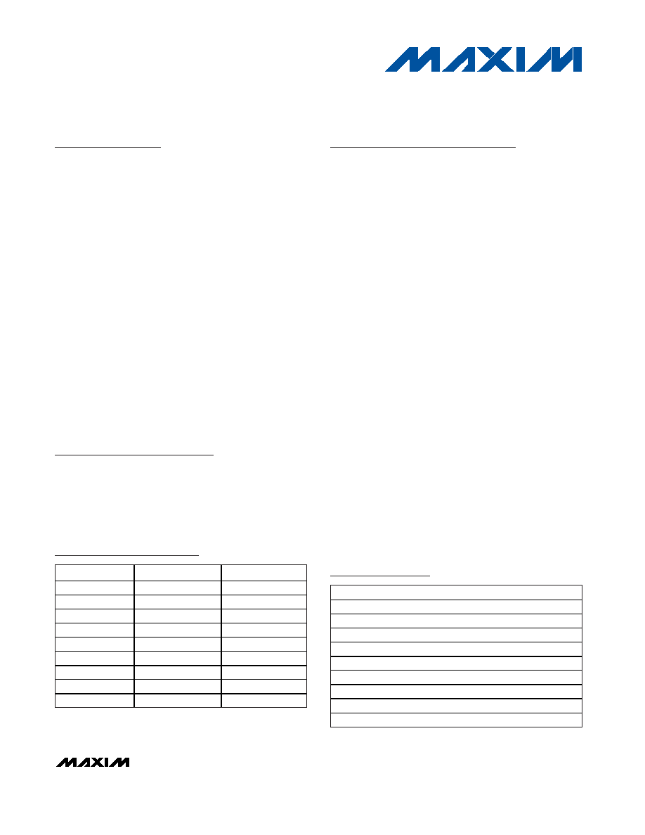
Ordering Information
Selector Guide
19-3157; Rev 2; 8/04
For pricing, delivery, and ordering information, please contact Maxim/Dallas Direct! at
1-888-629-4642, or visit Maxim's website at www.maxim-ic.com.
Pin Configurations and Typical Operating Circuits appear at
end of data sheet.
*Future product--contact factory for availability.
PART
TEMP RANGE
PIN-PACKAGE
MAX1316
ECM
-40
°C to +85°C
48 TQFP
MAX1317
ECM
-40
°C to +85°C
48 TQFP
MAX1318
ECM
-40
°C to +85°C
48 TQFP
MAX1320
ECM
-40
°C to +85°C
48 TQFP
MAX1321
ECM
-40
°C to +85°C
48 TQFP
MAX1322
ECM
-40
°C to +85°C
48 TQFP
MAX1324
ECM
-40
°C to +85°C
48 TQFP
MAX1325
ECM
-40
°C to +85°C
48 TQFP
MAX1326
ECM
-40
°C to +85°C
48 TQFP
PART
INPUT RANGE (V)
CHANNEL COUNT
MAX1316ECM
0 to +5
8
MAX1317ECM
0 to +5
4
MAX1318ECM
0 to +5
2
MAX1320ECM
±5
8
MAX1321ECM
±5
4
MAX1322ECM
±5
2
MAX1324ECM
±10
8
MAX1325ECM
±10
4
MAX1326ECM
±10
2
MAX1316MAX1318/MAX1320MAX1322/MAX1324MAX1326
8-/4-/2-Channel, 14-Bit, Simultaneous-Sampling ADCs
with ±10V, ±5V, and 0 to +5V Analog Input Ranges
2
_______________________________________________________________________________________
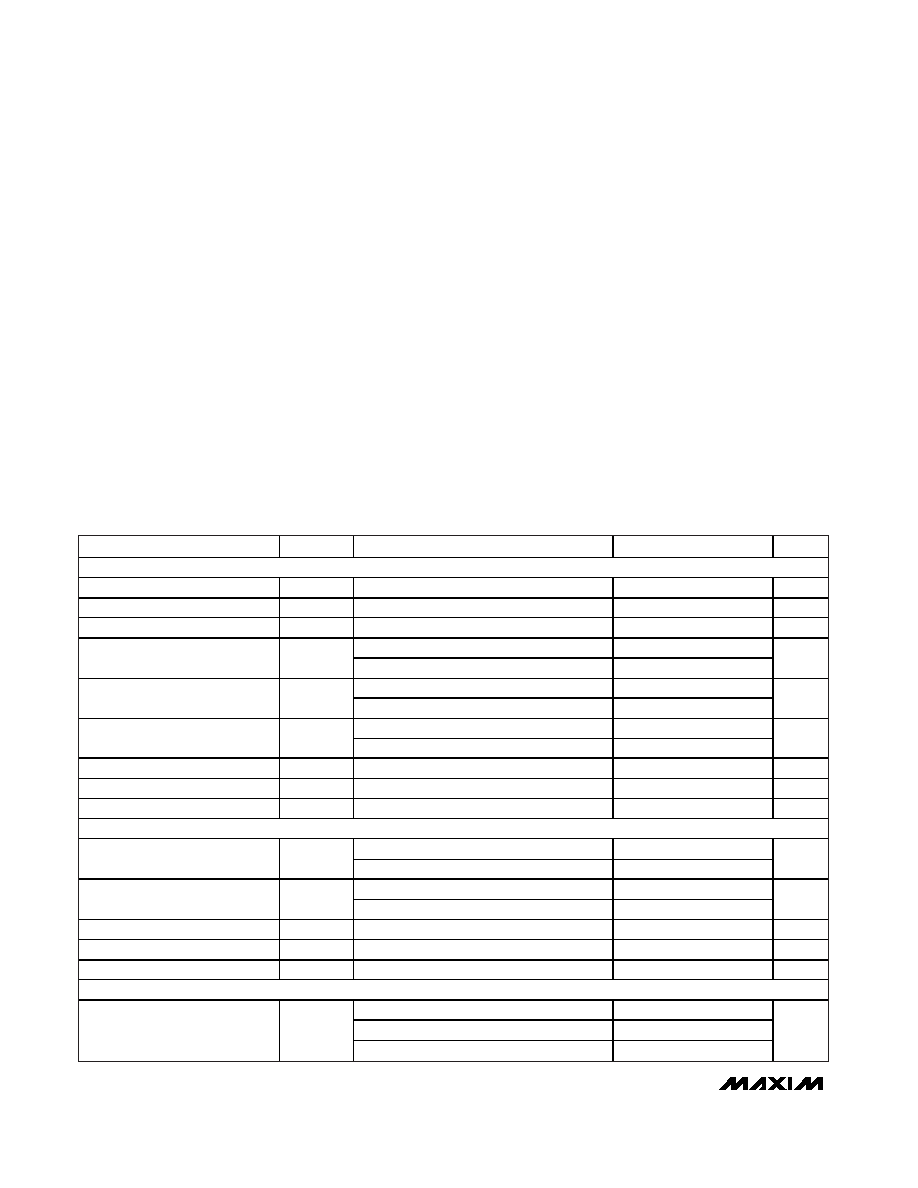
ABSOLUTE MAXIMUM RATINGS
ELECTRICAL CHARACTERISTICS
(AV
DD
= +5V, DV
DD
= +3V, AGND = DGND = 0V, V
REF
= V
REFMS
= +2.5V (external reference), C
REF
= C
REFMS
= 0.1µF, C
REF+
=
C
REF-
= 0.1µF, C
REF+-to-REF-
= 2.2µF || 0.1µF, C
COM
= 2.2µF || 0.1µF, C
MSV
= 2.2µF || 0.1µF (unipolar devices, MAX1316/
MAX1317/MAX1318), MSV = AGND (bipolar devices, MAX1320/MAX1321/MAX1322/MAX1324/MAX1325/MAX1326), f
CLK
= 10MHz,
50% duty cycle, INTCLK/
EXTCLK = AGND (external clock), SHDN = DGND, T
A
= T
MIN
to T
MAX
, unless otherwise noted. Typical val-
ues are at T
A
= +25°C.)
Stresses beyond those listed under "Absolute Maximum Ratings" may cause permanent damage to the device. These are stress ratings only, and functional
operation of the device at these or any other conditions beyond those indicated in the operational sections of the specifications is not implied. Exposure to
absolute maximum rating conditions for extended periods may affect device reliability.
AV
DD
to AGND .........................................................-0.3V to +6V
DV
DD
to DGND.........................................................-0.3V to +6V
AGND to DGND.....................................................-0.3V to +0.3V
CH0CH7, I.C. to AGND (MAX1316/MAX1317/MAX1318)...±6.0V
CH0CH7, I.C. to AGND (MAX1320/MAX1321/MAX1322).±16.5V
CH0CH7, I.C. to AGND (MAX1324/MAX1325/MAX1326).±16.5V
INTCLK/EXTCLK to AGND .......................-0.3V to (AV
DD
+ 0.3V)
EOC, EOLC, WR, RD, CS to DGND.........-0.3V to (DV
DD
+ 0.3V)
CONVST, CLK, SHDN,
ALLON to DGND..................................-0.3V to (DV
DD
+ 0.3V)
MSV, REF
MS
, REF to AGND.....................-0.3V to (AV
DD
+ 0.3V)
REF+, COM, REF- to AGND.....................-0.3V to (AV
DD
+ 0.3V)
D0D13 to DGND ....................................-0.3V to (DV
DD
+ 0.3V)
Maximum Current into Any Pin Except AV
DD
, DV
DD
,
AGND, DGND...............................................................±50mA
Continuous Power Dissipation
TQFP (derate 22.7mW/°C above +70°C) ...................1818mW
Operating Temperature Range ...........................-40°C to +85°C
Junction Temperature ......................................................+150°C
Storage Temperature Range .............................-65°C to +150°C
Lead Temperature (soldering, 10s) .................................+300°C
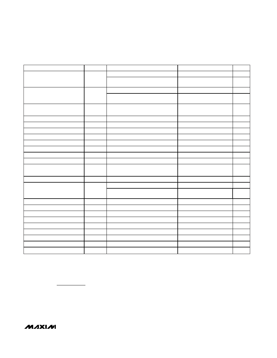
PARAMETER
SYMBOL
CONDITIONS
MIN
TYP
MAX
UNITS
STATIC PERFORMANCE (Note 1)
Resolution
N
14
Bits
Integral Nonlinearity
INL
(Note 2)
±0.8
±2.0
LSB
Differential Nonlinearity
DNL
No missing codes (Note 2)
±0.5
±1
LSB
Unipolar devices
±40
Offset Error
Bipolar devices
±40
LSB
Unipolar devices
-4
Offset Drift
Bipolar devices
-4
ppm/
°C
Unipolar devices between all channels
35
80
Channel Offset Matching
Bipolar devices between all channels
25
60
LSB
Gain Error
(Note 3)
±8
±40
LSB
Channel Gain-Error Matching
Between all channels
25
LSB
Gain Temperature Coefficient
3
ppm/
°C
DYNAMIC PERFORMANCE (at f
IN
= 100kHz, -0.4dB FS)
Unipolar
74.5
76
Signal-to-Noise Ratio
SNR
Bipolar
75
76.5
dB
Unipolar
74.5
76
Signal-to-Noise and Distortion
Ratio
SINAD
Bipolar
75
76.5
dB
Spurious-Free Dynamic Range
SFDR
83
93
dBc
Total Harmonic Distortion
THD
-90
-83
dBc
Channel-to-Channel Isolation
83
dB
ANALOG INPUTS (CH0CH7)
MAX1316/MAX1317/MAX1318
0
+5
MAX1320/MAX1321/MAX1322
-5
+5
Input Voltage Range
MAX1324/MAX1325/MAX1326
-10
+10
V
MAX1316MAX1318/MAX1320MAX1322/MAX1324MAX1326
8-/4-/2-Channel, 14-Bit, Simultaneous-Sampling ADCs
with ±10V, ±5V, and 0 to +5V Analog Input Ranges
_______________________________________________________________________________________
3
ELECTRICAL CHARACTERISTICS (continued)
(AV
DD
= +5V, DV
DD
= +3V, AGND = DGND = 0V, V
REF
= V
REFMS
= +2.5V (external reference), C
REF
= C
REFMS
= 0.1µF, C
REF+
=
C
REF-
= 0.1µF, C
REF+-to-REF-
= 2.2µF || 0.1µF, C
COM
= 2.2µF || 0.1µF, C
MSV
= 2.2µF || 0.1µF (unipolar devices, MAX1316/
MAX1317/MAX1318), MSV = AGND (bipolar devices, MAX1320/MAX1321/MAX1322/MAX1324/MAX1325/MAX1326), f
CLK
= 10MHz,
50% duty cycle, INTCLK/EXTCLK = AGND (external clock), SHDN = DGND, T
A
= T
MIN
to T
MAX
, unless otherwise noted. Typical val-
ues are at T
A
= +25°C.)
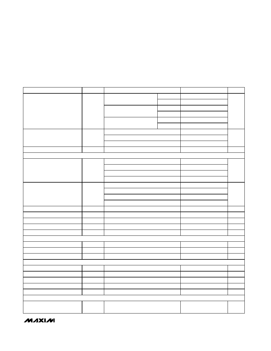
PARAMETER
SYMBOL
CONDITIONS
MIN
TYP
MAX
UNITS
V
IN
= +5V
0.54
0.72
MAX1316/MAX1317/MAX1318
V
IN
= 0V
-0.157
-0.12
V
IN
= +5V
0.29
0.39
MAX1320/MAX1321/MAX1322
V
IN
= -5V
-1.16
-0.87
V
IN
= +10V
0.56
0.74
Input Current (Note 4)
MAX1324/MAX1325/MAX1326
V
IN
= -10V
-1.13
-0.85
mA
MAX1316/MAX1317/MAX1318
7.58
MAX1320/MAX1321/MAX1322
8.66
Input Resistance (Note 4)
MAX1324/MAX1325/MAX1326
14.26
Input Capacitance
15
pF
TRACK/HOLD
One channel
526
Two channels
455
Four channels
357
External-Clock Throughput Rate
(Note 5)
Eight channels
250
ksps
One channel (INTCLK/EXTCLK = AV
DD
)
526
Two channels (INTCLK/EXTCLK = AV
DD
)
455
Four channels (INTCLK/EXTCLK = AV
DD
)
357
Internal-Clock Throughput Rate
(Note 5)
Eight channels (INTCLK/EXTCLK = AV
DD
)
250
ksps
Small-Signal Bandwidth
10
MHz
Full-Power Bandwidth
10
MHz
Aperture Delay
16
ns
Aperture Jitter
50
ps
RMS
Aperture-Delay Matching
100
ps
INTERNAL REFERENCE
REFMS Voltage
V
REFMS
2.475
2.500
2.525
V
REF Voltage
V
REF
2.475
2.500
2.525
V
REF Temperature Coefficient
30
ppm/
°C
EXTERNAL REFERENCE (REF
MS
AND REF EXTERNALLY DRIVEN)
Input Current
-250
+250
µA
REFMS Input Voltage Range
V
REFMS
Unipolar devices
2.0
2.5
3.0
V
REF Voltage Input Range
V
REF
2.0
2.5
3.0
V
REF Input Capacitance
15
pF
REFMS Input Capacitance
15
pF
DIGITAL INPUTS (D0D7,
RD
,
WR
,
CS
, CLK, SHDN, ALLON, CONVST)
Input-Voltage High
V
IH
0.7 x
DV
DD
V
MAX1316MAX1318/MAX1320MAX1322/MAX1324MAX1326
8-/4-/2-Channel, 14-Bit, Simultaneous-Sampling ADCs
with ±10V, ±5V, and 0 to +5V Analog Input Ranges
4
_______________________________________________________________________________________
ELECTRICAL CHARACTERISTICS (continued)
(AV
DD
= +5V, DV
DD
= +3V, AGND = DGND = 0V, V
REF
= V
REFMS
= +2.5V (external reference), C
REF
= C
REFMS
= 0.1µF, C
REF+
=
C
REF-
= 0.1µF, C
REF+-to-REF-
= 2.2µF || 0.1µF, C
COM
= 2.2µF || 0.1µF, C
MSV
= 2.2µF || 0.1µF (unipolar devices, MAX1316/
MAX1317/MAX1318), MSV = AGND (bipolar devices, MAX1320/MAX1321/MAX1322/MAX1324/MAX1325/MAX1326), f
CLK
= 10MHz,
50% duty cycle, INTCLK/EXTCLK = AGND (external clock), SHDN = DGND, T
A
= T
MIN
to T
MAX
, unless otherwise noted. Typical val-
ues are at T
A
= +25°C.)
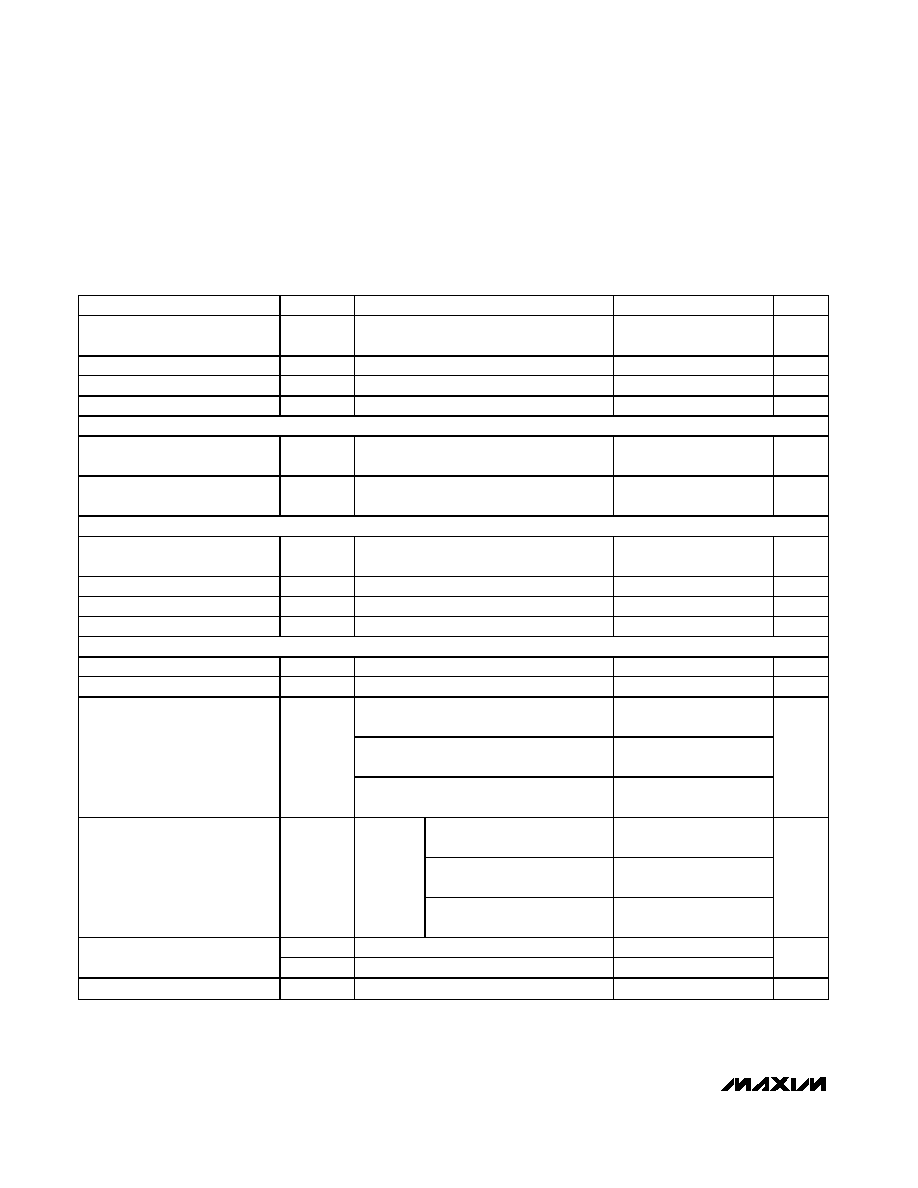
PARAMETER
SYMBOL
CONDITIONS
MIN
TYP
MAX
UNITS
Input-Voltage Low
V
IL
0.3 x
DV
DD
V
Input Hysteresis
15
mV
Input Capacitance
C
IN
15
pF
Input Current
I
IN
V
IN
= 0V or DV
DD
±1
µA
CLOCK-SELECT INPUT (INTCLK/
EXTCLK
)
Input-Voltage High
0.7 x
AV
DD
V
Input-Voltage Low
0.3 x
AV
DD
V
DIGITAL OUTPUTS (D0D13,
EOC
,
EOLC
)
Output-Voltage High
V
OH
ISOURCE = 0.8mA
DV
DD
-
0.6
V
Output-Voltage Low
V
OL
ISINK = 1.6mA
0.4
V
Tri-State Leakage Current
RD
V
IH
or CS
V
IH
0.06
1
µA
Tri-State Output Capacitance
RD
V
IH
or CS
V
IH
15
pF
POWER SUPPLIES
Analog-Supply Voltage
AV
DD
4.75
5.25
V
Digital-Supply Voltage
DV
DD
2.70
5.25
V
MAX1316/MAX1317/MAX1318, all channels
selected
46
51
MAX1320/MAX1321/MAX1322, all channels
selected
46
51
Analog-Supply Current
I
AVDD
MAX1324/MAX1325/MAX1326, all channels
selected
46
51
mA
MAX1316/MAX1317/MAX1318,
all channels selected
1
1.6
MAX1320/MAX1321/MAX1322,
all channels selected
1
1.6
Digital-Supply Current (Note 6)
I
DVDD
C
LOAD
=
100pF
MAX1324/MAX1325/MAX1326,
all channels selected
1
1.6
mA
I
AVDD
V
SHDN
= DV
DD
, V
CH
= float
10
Shutdown Current (Note 7)
I
DVDD
V
RD
= V
WR
= DV
DD
, V
SHDN
= DV
DD
0.1
2
µA
Power-Supply Rejection Ratio
PSRR
AV
DD
= +4.75V to +5.75V (Note 8)
50
dB
MAX1316MAX1318/MAX1320MAX1322/MAX1324MAX1326
8-/4-/2-Channel, 14-Bit, Simultaneous-Sampling ADCs
with ±10V, ±5V, and 0 to +5V Analog Input Ranges
_______________________________________________________________________________________
5
Note 1:
For the MAX1316/MAX1317/MAX1318, V
IN
= 0 to +5V. For the MAX1320/MAX1321/MAX1322, V
IN
= -5V to +5V. For the
MAX1324/MAX1325/MAX1326, V
IN
= -10V to +10V.
Note 2:
All channel performance is guaranteed by correlation to a single channel test.
Note 3:
Offset nulled.
Note 4:
The analog input resistance is terminated to an internal bias point. Calculate the analog input current using:
for V
CH
within the input voltage range.
Note 5:
Throughput rate is given per channel. Throughput rate is a function of clock frequency (f
CLK
= 10MHz). See the Data
Throughput section for more information.
Note 6:
All analog inputs are driven with an FS 100kHz sine wave.
I
V
V
R
CH
CH
BIAS
CH
_
_
_
=
-
TIMING CHARACTERISTICS (Figures 3, 4, 5, 6 and 7) (Tables 1, 3)
PARAMETER
SYMBOL
CONDITIONS
MIN
TYP
MAX
UNITS
Internal clock
1.6
1.8
µs
Time-to-First-Conversion Result
t
CONV
External clock, Figure 6
16
Clock
cycles
Internal clock
0.3
0.36
µs
Time-to-Next-Conversion Result
t
NEXT
External clock, Figure 6
3
Clock
cycles
CONVST Pulse-Width Low
(Acquisition Time)
t
ACQ
(Note 9)
0.16
100
µs
CS Pulse Width
t
2
30
ns
RD Pulse-Width Low
t
3
30
ns
RD Pulse-Width High
t
4
30
ns
WR Pulse-Width Low
t
5
30
ns
CS to WR
t
6
(Note 10)
ns
WR to CS
t
7
(Note 10)
ns
CS to RD
t
8
(Note 10)
ns
RD to CS
t
9
(Note 10)
ns
Data-Access Time
(RD Low to Valid Data)
t
10
30
ns
Bus-Relinquish Time (RD High)
t
11
30
ns
Internal clock
80
ns
EOC Pulse Width
t
12
External clock, Figure 6
1
Clock
cycles
Input-Data Setup Time
t
14
10
ns
Input-Data Hold Time
t
15
10
ns
External-Clock Period
t
16
0.08
10.00
µs
External-Clock High Period
t
17
Logic sensitive to rising edges
20
ns
External-Clock Low Period
t
18
Logic sensitive to rising edges
20
ns
External-Clock Frequency
(Note 11)
0.1
12.5
MHz
Internal-Clock Frequency
10
MHz
CONVST High to CLK Edge
t
19
20
(Note 12)
ns
EOC Low to RD
t
20
0
ns