Äîêóìåíòàöèÿ è îïèñàíèÿ www.docs.chipfind.ru
General Description
The MAX1516/MAX1517/MAX1518 include a high-perfor-
mance step-up regulator, two linear-regulator controllers,
and high-current operational amplifiers for active-matrix
thin-film transistor (TFT) liquid-crystal displays (LCDs).
Also included is a logic-controlled, high-voltage switch
with adjustable delay.
The step-up DC-DC converter provides the regulated
supply voltage for the panel source driver ICs. The con-
verter is a high-frequency (1.2MHz) current-mode regu-
lator with an integrated 14V n-channel MOSFET that
allows the use of ultra-small inductors and ceramic
capacitors. It provides fast transient response to pulsed
loads while achieving efficiencies over 85%.
The gate-on and gate-off linear-regulator controllers
provide regulated TFT gate-on and gate-off supplies
using external charge pumps attached to the switching
node. The MAX1518 includes five high-performance
operational amplifiers, the MAX1517 includes three,
and the MAX1516 includes one operational amplifier.
These amplifiers are designed to drive the LCD back-
plane (VCOM) and/or the gamma-correction divider
string. The devices feature high output current
(±150mA), fast slew rate (13V/µs), wide bandwidth
(12MHz), and rail-to-rail inputs and outputs.
The MAX1516/MAX1517/MAX1518 are available in 32-
pin thin QFN packages with a maximum thickness of
0.8mm for ultra-thin LCD panels.
Applications
Notebook Computer Displays
LCD Monitor Panels
Automotive Displays
Features
2.6V to 5.5V Input Supply Range
1.2MHz Current-Mode Step-Up Regulator
Fast Transient Response to Pulsed Load
High-Accuracy Output Voltage (1.5%)
Built-In 14V, 2.4A, 0.16 N-Channel MOSFET
High Efficiency (90%)
Linear-Regulator Controllers for V
GON
and V
GOFF
High-Performance Operational Amplifiers
±150mA Output Short-Circuit Current
13V/µs Slew Rate
12MHz, -3dB Bandwidth
Rail-to-Rail Inputs/Outputs
Logic-Controlled, High-Voltage Switch with
Adjustable Delay
Timer-Delay Fault Latch for All Regulator Outputs
Thermal-Overload Protection
0.6mA Quiescent Current
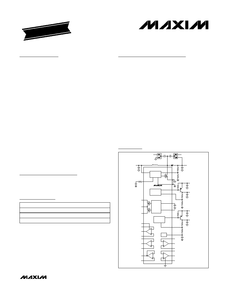
MAX1516/MAX1517/MAX1518
TFT-LCD DC-DC Converters with
Operational Amplifiers
________________________________________________________________
Maxim Integrated Products
1
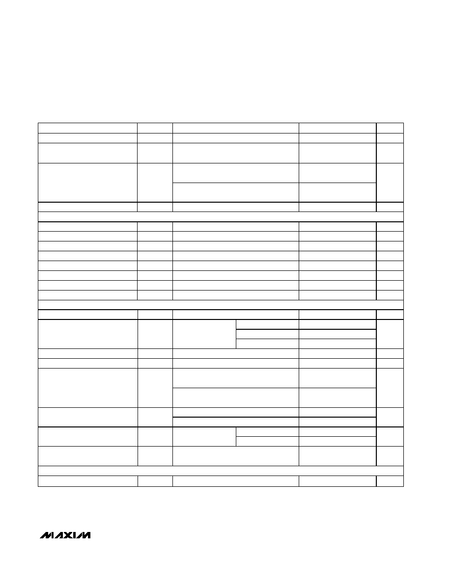
Ordering Information
STEP-UP
CONTROLLER
GATE-ON
CONTROLLER
SWITCH
CONTROL
GATE-OFF
CONTROLLER
REF
VCN
VCP
VMAIN
LX
FB
PGND
AGND
DRVP
FBP
VCP
VGON
VCN
VGOFF
DEL
CTL
DRVN
FBN
NEG4
REF
POS4
NEG5
POS5
OUT4
OUT5
BGND
NEG2
POS2
OP3
POS3
OUT2
OUT3
POS1
OUT1
NEG1
SUP
COM
DRN
SRC
COMP
IN
VIN
MAX1518
OP2
OP1
OP5
OP4
Minimal Operating Circuit
19-3244; Rev 0; 4/04
For pricing, delivery, and ordering information, please contact Maxim/Dallas Direct! at
1-888-629-4642, or visit Maxim's website at www.maxim-ic.com.
EVALUATION KIT
AVAILABLE
PART
TEMP RANGE
PIN-PACKAGE
MAX1516
ETJ
-40
°
C to +100
°
C
32 Thin QFN 5mm x 5mm
MAX1517
ETJ
-40
°
C to +100
°
C
32 Thin QFN 5mm x 5mm
MAX1518
ETJ
-40
°
C to +100
°
C
32 Thin QFN 5mm x 5mm
Pin Configurations appear at end of data sheet.
MAX1516/MAX1517/MAX1518
TFT-LCD DC-DC Converters with
Operational Amplifiers
2
_______________________________________________________________________________________
ABSOLUTE MAXIMUM RATINGS
Stresses beyond those listed under "Absolute Maximum Ratings" may cause permanent damage to the device. These are stress ratings only, and functional
operation of the device at these or any other conditions beyond those indicated in the operational sections of the specifications is not implied. Exposure to
absolute maximum rating conditions for extended periods may affect device reliability.
IN, CTL to AGND ......................................................-0.3V to +6V
COMP, FB, FBP, FBN, DEL, REF to AGND ....-0.3V to (V
IN
+ 0.3V)
PGND, BGND to AGND ......................................................±0.3V
LX to PGND ............................................................-0.3V to +14V
SUP to AGND .........................................................-0.3V to +14V
DRVP, SRC to AGND..............................................-0.3V to +30V
POS_, NEG_, OUT_ to AGND ...................-0.3V to (V
SUP
+ 0.3V)
POS1 to NEG1, POS2 to NEG2, POS3 to NEG3,
POS4 to NEG4, POS5 to NEG5 ...............................-6V to +6V
DRVN to AGND ...................................(V
IN
- 30V) to (V
IN
+ 0.3V)
COM, DRN to AGND ................................-0.3V to (V
SRC
+ 0.3V)
DRN to COM............................................................-30V to +30V
OUT_ Maximum Continuous Output Current....................±75mA
LX Switch Maximum Continuous RMS Output Current .........1.6A
Continuous Power Dissipation (T
A
= +70°C)
32-Pin Thin QFN (derate 21.2mW/°C above +70°C) ..1702mW
Operating Temperature Range .........................-40°C to +100°C
Junction Temperature ......................................................+150°C
Storage Temperature Range .............................-65°C to +150°C
Lead Temperature (soldering, 10s) .................................+300°C
ELECTRICAL CHARACTERISTICS
(V
IN
= 3V, V
SUP
= 8V, PGND = AGND = BGND = 0, I
REF
= 25µA,
T
A
= 0°C to +85°C. Typical values are at T
A
= +25°C, unless other-
wise noted.)
PARAMETER
SYMBOL
CONDITIONS
MIN
TYP
MAX
UNITS
IN Supply Range
V
IN
2.6
5.5
V
IN Undervoltage-Lockout
Threshold
V
UVLO
V
IN
rising, typical hysteresis = 150mV
2.3
2.5
2.7
V
V
FB
= V
FBP
= 1.4V, V
FBN
= 0,
LX not switching
0.6
0.8
IN Quiescent Current
I
IN
V
FB
= 1.1V, V
FBP
= 1.4V, V
FBN
= 0,
LX switching
6
11
mA
Duration to Trigger Fault
Condition
55
ms
REF Output Voltage
-2µA < I
REF
< 50µA, V
IN
= 2.6V to 5.5V
1.231
1.250
1.269
V
Temperature rising
+160
Thermal Shutdown
Hysteresis
15
°
C
MAIN STEP-UP REGULATOR
Output Voltage Range
V
MAIN
V
IN
13
V
Operating Frequency
f
OSC
1020
1200
1380
kHz
Oscillator Maximum Duty Cycle
84
87
90
%
T
A
= +25
°
C to +85
°
C
1.221
1.233
1.245
FB Regulation Voltage
V
FB
No load
T
A
= 0
°
C to +85
°
C
1.218
1.233
1.247
V
FB Fault Trip Level
V
FB
falling
0.96
1.00
1.04
V
FB Load Regulation
0 < I
MAIN
< full load, transient only
-1.6
%
FB Line Regulation
V
IN
= 2.6V to 5.5V
+0.04
±
0.15
%/
V
FB Input Bias Current
V
FB
= 1.4V
-40
+40
nA
FB Transconductance
I
COMP
= 5µA
75
150
280
µS
FB Voltage Gain
FB to COMP
600
V/
V
MAX1516/MAX1517/MAX1518
TFT-LCD DC-DC Converters with
Operational Amplifiers
_______________________________________________________________________________________
3
ELECTRICAL CHARACTERISTICS (continued)
(V
IN
= 3V, V
SUP
= 8V, PGND = AGND = BGND = 0, I
REF
= 25µA,
T
A
= 0°C to +85°C. Typical values are at T
A
= +25°C, unless other-
wise noted.)
PARAMETER
SYMBOL
CONDITIONS
MIN
TYP
MAX
UNITS
LX On-Resistance
R
LX(ON)
160
250
m
LX Leakage Current
I
LX
V
LX
= 13V
0.02
40
µA
LX Current Limit
I
LIM
V
FB
= 1V, duty cycle = 65%
2.5
3.0
3.5
A
Current-Sense
Transconductance
3.0
3.8
5
S
Soft-Start Period
t
SS
14
ms
Soft-Start Step Size
I
LIM
/ 8
A
OPERATIONAL AMPLIFIERS
SUP Supply Range
V
SUP
4.5
13.0
V
MAX1518
3.2
4.8
MAX1517
2
3
SUP Supply Current
I
SUP
Buffer configuration,
V
POS
_ = 4V, no load
MAX1516
0.7
1.1
mA
Input Offset Voltage
V
OS
(V
NEG
_, V
POS
_, V
OUT
_)
V
SUP
/ 2,
T
A
= +25
°
C
0
12
mV
Input Bias Current
I
BIAS
(V
NEG
_ , V
POS
_, V
OUT
_)
V
SUP
/ 2
+1
±
50
nA
Input Common-Mode Range
V
CM
0
V
SUP
V
Common-Mode Rejection Ratio
CMRR
0
(V
NEG
_, V
POS
_)
V
SUP
45
dB
Open-Loop Gain
125
dB
I
OUT
_ = 100µA
V
SUP
-
15
V
SUP
-
3
Output Voltage Swing, High
V
OH
I
OUT
_ = 5mA
V
SUP
-
150
V
SUP
-
80
mV
I
OUT
_ = -100µA
2
15
Output Voltage Swing, Low
V
OL
I
OUT
_ = -5mA
70
150
mV
Short-Circuit Current
To V
SUP
/ 2, source or sink
50
150
mA
Output Source and Sink Current
(V
NEG
_ , V
POS
_, V
OUT
_)
V
SUP
/ 2,
|
V
OS
| < 10mV
40
mA
Power-Supply Rejection Ratio
PSRR
DC, 6V
V
SUP
13V,
(V
NEG
_, V
POS
_)
V
SUP
/2
60
dB
Slew Rate
13
V/µs
-3dB Bandwidth
R
L
= 10k
, C
L
= 10pF, buffer configuration
12
MHz
Gain-Bandwidth Product
GBW
Buffer configuration
8
MHz
GATE-ON LINEAR-REGULATOR CONTROLLER
FBP Regulation Voltage
V
FBP
I
DRVP
= 100µA
1.231
1.250
1.269
V
FBP Fault Trip Level
V
FBP
falling
0.96
1.00
1.04
V
FBP Input Bias Current
I
FBP
V
FBP
= 1.4V
-50
+50
nA
FBP Effective Load-Regulation
Error (Transconductance)
V
DRVP
= 10V, I
DRVP
= 50µA to 1mA
-0.7
-1.5
%
MAX1516/MAX1517/MAX1518
TFT-LCD DC-DC Converters with
Operational Amplifiers
4
_______________________________________________________________________________________
ELECTRICAL CHARACTERISTICS (continued)
(V
IN
= 3V, V
SUP
= 8V, PGND = AGND = BGND = 0, I
REF
= 25µA,
T
A
= 0°C to +85°C. Typical values are at T
A
= +25°C, unless other-
wise noted.)
PARAMETER
SYMBOL
CONDITIONS
MIN
TYP
MAX
UNITS
FBP Line (IN) Regulation Error
I
DRVP
= 100µA, 2.6V < V
IN
< 5.5V
±1.5
±5
mV
DRVP Sink Current
I
DRVP
V
FBP
= 1.1V, V
DRVP
= 10V
1
5
mA
DRVP Off-Leakage Current
V
FBP
= 1.4V, V
DRVP
= 28V
0.01
10
µA
Soft-Start Period
t
SS
14
ms
Soft-Start Step Size
V
REF
/
128
V
GATE-OFF LINEAR-REGUALTOR CONTROLLER
FBN Regulation Voltage
V
FBN
I
DRVN
= 100µA
235
250
265
mV
FBN Fault Trip Level
V
FBN
rising
370
420
470
mV
FBN Input Bias Current
I
FBN
V
FBN
= 0
-50
+50
nA
FBN Effective Load-Regulation
Error (Transconductance)
V
DRVN
= -10V, I
DRVN
= 50µA to 1mA
11
25
mV
FBN Line (IN) Regulation Error
I
DRVN
= 0.1mA, 2.6V < V
IN
< 5.5V
+0.7
±5
mV
DRVN Source Current
I
DRVN
V
FBN
= 500mV, V
DRVN
= -10V
1
4
mA
DRVN Off-Leakage Current
V
FBN
= 0V, V
DRVN
= -25V
-0.01
-10
µA
Soft-Start Period
t
SS
14
ms
Soft-Start Step Size
V
REF
/
128
V
POSITIVE GATE-DRIVER TIMING AND CONTROL SWITCHES
DEL Capacitor Charge Current
During startup, V
DEL
= 1V
4
5
6
µA
DEL Turn-On Threshold
V
TH(DEL)
1.19
1.25
1.31
V
DEL Discharge Switch On-
Resistance
During UVLO, V
IN
= 2.2V
20
CTL Input Low Voltage
V
IN
= 2.6V to 5.5V
0.6
V
CTL Input High Voltage
V
IN
= 2.6V to 5.5V
2
V
CTL Input Leakage Current
CTL = AGND or IN
-1
+1
µA
CTL-to-SRC Propagation Delay
100
ns
SRC Input Voltage Range
28
V
V
DEL
= 1.5V, CTL = IN
50
100
SRC Input Current
I
SRC
V
DEL
= 1.5V, CTL = AGND
15
30
µA
SRC to COM Switch On-
Resistance
R
SRC(ON)
V
DEL
= 1.5V, CTL = IN
6
12
DRN to COM Switch On-
Resistance
R
DRN(ON)
V
DEL
= 1.5V, CTL = AGND
35
70
COM to PGND Switch On-
Resistance
R
COM(ON)
V
DEL
= 1.1V
350
1000
1800
MAX1516/MAX1517/MAX1518
TFT-LCD DC-DC Converters with
Operational Amplifiers
_______________________________________________________________________________________
5
ELECTRICAL CHARACTERISTICS
(V
IN
= 3V, V
SUP
= 8V, PGND = AGND = BGND = 0, I
REF
= 25µA,
T
A
= -40°C to +85°C, unless otherwise noted.) (Note 1)
PARAMETER
SYMBOL
CONDITIONS
MIN
MAX
UNITS
IN Supply Range
V
IN
2.6
5.5
V
IN Undervoltage-Lockout
Threshold
V
UVLO
V
IN
rising, typical hysteresis = 150mV
2.265
2.715
V
V
FB
= V
FBP
= 1.4V, V
FBN
= 0,
LX not switching
0.8
IN Quiescent Current
I
IN
V
FB
= 1.1V, V
FBP
= 1.4V, V
FBN
= 0,
LX switching
11
mA
REF Output Voltage
-2µA < I
REF
< 50µA, V
IN
= 2.6V to 5.5V
1.222
1.269
V
MAIN STEP-UP REGULATOR
Output Voltage Range
V
MAIN
V
IN
13
V
Operating Frequency
f
OSC
1020
1380
kHz
FB Regulation Voltage
V
FB
No load
1.212
1.250
V
FB Line Regulation
V
IN
= 2.6V to 5.5V
±
0.15
%/
V
FB Input Bias Current
V
FB
= 1.4V
-40
+40
nA
FB Transconductance
I
COMP
= 5µA
75
300
µS
LX On-Resistance
R
LX(ON)
250
m
LX Current Limit
I
LIM
V
FB
= 1V, duty cycle = 65%
2.5
3.5
A
OPERATIONAL AMPLIFIERS
SUP Supply Range
V
SUP
4.5
13.0
V
MAX1518
4.8
MAX1517
3.0
SUP Supply Current
I
SUP
Buffer configuration,
V
POS
_ = 4V, no load
MAX1516
1.1
mA
Input Offset Voltage
V
OS
(V
NEG
_, V
POS
_, V
OUT
_)
V
SUP
/ 2
12
mV
Input Common-Mode Range
V
CM
0
V
SUP
V
I
OUT
_ = 100µA
V
SUP
-
15
Output Voltage Swing, High
V
OH
I
OUT
_ = 5mA
V
SUP
-
150
mV
I
OUT
_ = -100µA
15
Output Voltage Swing, Low
V
OL
I
OUT
_ = -5mA
150
mV
Source
50
Short-Circuit Current
To V
SUP
/ 2
Sink
50
mA
Output Source and Sink Current
(V
NEG
_ , V
POS
_, V
OUT
_)
V
SUP
/ 2,
|
V
OS
| < 10mV
40
mA
GATE-ON LINEAR-REGULATOR CONTROLLER
FBP Regulation Voltage
V
FBP
I
DRVP
= 100µA
1.218
1.269
V