
General Description
The MAX2116/MAX2118 family of low-cost direct-
conversion tuner ICs are designed for use in digital
direct broadcast satellite (DBS) television applications,
professional VSAT systems, and two-way Internet
through satellite applications. These devices set the
standard for integration and performance, significantly
reducing the required RF know-how for design imple-
mentation. Uniquely architected, the MAX2116/MAX2118
simplify direct main board and tuner module designs.
The MAX2116/MAX2118 devices directly convert L-
band signals to baseband using a broadband I/Q
downconverter. The operating frequency range extends
from 925MHz to 2175MHz.
Each IC includes an LNA with gain control, I and Q
downconverting mixers, and baseband lowpass filters
gain and cutoff frequency control. Together, the RF and
baseband variable gain amplifiers provide more than
79dB of gain control range.
The devices include fully monolithic VCOs, as well as a
complete frequency synthesizer. Additionally, an on-
chip crystal oscillator is provided along with a buffered
output for driving additional tuners and demodulators.
Synthesizer programming and device configuration are
accomplished with a 2-wire serial interface. For multi-
tuner applications, each device can be configured to
have one of eight possible 2-wire interface addresses.
Simplifying the interface to low-voltage CMOS demodu-
lators, the MAX2116/MAX2118 incorporate two 2.85V
regulated outputs for pulling up open-drain interface
connections, thus preventing noisy 3V rails from cor-
rupting the sensitive analog signal of the tuners.
The MAX2116/MAX2118 devices are the most versatile
family of DBS products available. With both single-
ended and differential baseband outputs, these
devices are compatible with virtually all QPSK/8-PSK
demodulators. The tuners are available in a very small
40-pin QFN package.
Applications
DVB
DSS (U.S.)
VSAT
Internet Through Satellite
Features
o Fully Integrated VCOs
o Supports 1Mbaud to 45Mbaud, 925MHz to
2175MHz Operation
o 4MHz to 33MHz Tunable LP Filters
o Complete Synthesizer with I
2
CTM Interface
o Analog RF VGA and Digital Baseband VGA
o Multiple I
2
C Addresses for Multituner
Applications
o Single-Ended (MAX2116) and Differential
(MAX2118) I/Q Interface
MAX2116/MAX2118
Complete DBS Direct-Conversion Tuner ICs
with Monolithic VCOs
19-2433; Rev 0; 4/02
For pricing, delivery, and ordering information, please contact Maxim/Dallas Direct! at
1-888-629-4642, or visit Maxim's website at www.maxim-ic.com.
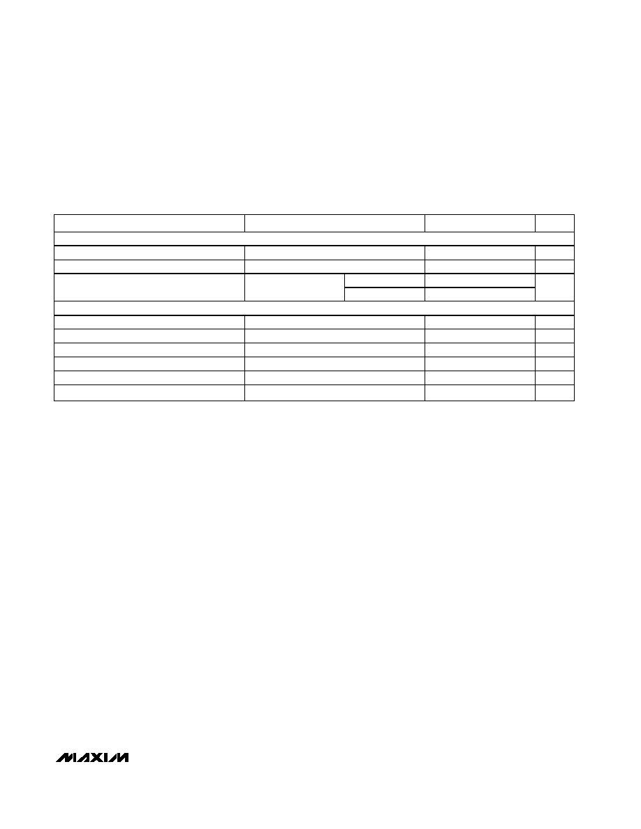
Ordering Information
PART
TEMP RANGE
PIN-PACKAGE
MAX2116UGL
0∞C to +85∞C
40 QFN-EP* (6mm
6mm)
MAX2118UGL
0∞C to +85∞C
40 QFN-EP* (6mm
6mm)
________________________________________________________________ Maxim Integrated Products
1
*EP = exposed pad.
1
2
3
4
5
6
7
8
9
10
30
29
28
27
26
25
24
23
22
21
11
12
13
14
15
16
17
18
19
20
40
39
38
37
36
35
34
33
32
31
DIV2/
DIV4
GC2
DAC
/N
/R
PFD
CP
DC OFFSET
CORRECTION
VOLTAGE
REGULATOR
INTERFACE LOGIC
AND CONTROL
LPF BW
CONTROL
ADC
TANK
TANK
TANK
TANK
TANK
TANK
TANK
TANK
IDC-
IDC+
VCCRF1
RFIN-
RFIN+
N.C.
GC1
VREG1
N.C.
PAD
N.C.
VCCLO
VCCVCO
LOFL
T
AS2
VTUNE
CPOUT
IFL
T
VCCCPX
CFL
T
XTAL+
AS1
N.C.
XTALOUT
CNTOUT
XTAL-
SCL
VREG2
SDA
VCCDIG
N.C.
VCCBB
QOUT+
QOUT
-
(MAX2118 ONL
Y
)
AS0
QDC-
QDC+
VCCRF2
IOUT+
IOUT
-
(MAX2118 ONL
Y
)
MAX2118
Pin Configuration/
Functional Diagram
I
2
C is a trademark of Philips Corp.

MAX2116/MAX2118
Complete DBS Direct-Conversion Tuner ICs
with Monolithic VCOs
2
_______________________________________________________________________________________
ABSOLUTE MAXIMUM RATINGS
Stresses beyond those listed under "Absolute Maximum Ratings" may cause permanent damage to the device. These are stress ratings only, and functional
operation of the device at these or any other conditions beyond those indicated in the operational sections of the specifications is not implied. Exposure to
absolute maximum rating conditions for extended periods may affect device reliability.
V
CC
to GND ...........................................................-0.3V to +5.5V
All Other Pins to GND .................................-0.3V to (V
CC
+ 0.3V)
RFIN+ to RFIN-, XTL+ to XTL-, IDC+ to IDC-,
QDC+ to QDC- ...................................................................±2.0V
CNTOUT, XTALOUT, CPOUT, VREG1/2,
I/QOUT± to GND Short-Circuit Duration.................................10s
Continuous Current (any pin other than V
CC
or GND) .......10mA
Continuous Power Dissipation (T
A
= +85∞C)
40-pin QFN (derate 23.3mW/∞C above +85∞C) ............ 1.86W
Operating Temperature Range ..............................0∞C to +85∞C
Junction Temperature .....................................................+150∞C
Storage Temperature Range ............................-65∞C to +160∞C
Soldering Temperature (10s) ..........................................+300∞C
DC ELECTRICAL CHARACTERISTICS
(V
CC
= +4.75V to +5.25V, GND = 0V, GC1 = +0.75V; no AC signal applied, default register settings, T
A
= 0∞C to +85∞C, unless other-
wise noted. Typical values are at V
CC
= +5V, T
A
= +25∞C, unless otherwise noted.) (Note 1)
PARAMETER
CONDITIONS
MIN
TYP
MAX
UNITS
SUPPLY
Supply Voltage
4.75
5.25
V
Supply Current
LO locked at 2175MHz
195
265
mA
ANALOG GAIN CONTROL INPUT--GC1
Usable Voltage Range
0.75
2.6
V
Input Current
0.75V < GC1 < 2.6V (Note 2)
-50
+50
µA
BASEBAND OUTPUTS-- IOUT, QOUT (MAX2116)
Nominal Output Voltage Swing
R
LOAD
= 1k
// 10pF (Note 3)
0.8
V
P-P
Output Clipping Voltage
2
V
P-P
DC Output Voltage
1.2
V
BASEBAND OUTPUTS-- IOUT±, QOUT± (MAX2118)
Bit DL = high
1
Nominal Output Voltage Swing
R
LOAD
= 2k
// 10pF
(differential) (Note 3)
Bit DL = low
0.59
V
P-P
Output Clipping Voltage
2
V
P-P
Common-Mode Voltage
0.65
0.75
0.85
V
DC Offset Voltage
-50
0
+50
mV
ANALOG OUTPUT-- VREG1, VREG2
Output Voltage
2.7
2.85
3.05
V
Source Current
Each output
3
mA
STATIC CONTROL INPUTS--AS2, AS1, AS0
Input Voltage High
4
V
Input Voltage Low
0.5
V
Input Current
-50
+50
µA
SYNTHESIZER DC PARAMETERS
Bits CP1 = 0, CP0 = 0
±35
±50
±68
Bits CP1 = 0, CP0 = 1
±70
±100
±136
Bits CP1 = 1, CP0 = 0
±140
±200
±272
Charge Pump Source/Sink Current
Bits CP1 = 1, CP0 = 1
±280
±400
±544
µA

MAX2116/MAX2118
Complete DBS Direct-Conversion Tuner ICs
with Monolithic VCOs
_______________________________________________________________________________________
3
AC ELECTRICAL CHARACTERISTICS
(MAX2116/MAX2118 EV kits, V
CC
= +4.75V to +5.25V, GC1 and GC2 set for maximum gain, GND = 0V, IOUT = QOUT = 800mV
P-P
(MAX2116), loaded with 1k
IOUT± = QOUT± = 590mV
P-P
differential (DL = 0, MAX2118), IOUT
± = QOUT± = 1V
P-P
differential (DL
= 1, MAX2118), loaded with differential 2k
. Baseband LPF BW = 33MHz, f
RFIN
= 2175MHz. For default register values, see the
Serial Interface and Control Registers section. T
A
= +25∞C to +85∞C. Typical values are at V
CC
= +5V, T
A
= +25∞C, unless otherwise
noted.) (Note 1)
PARAMETER
CONDITIONS
MIN
TYP
MAX
UNITS
RF FRONT END
RF Input Frequency Range
T
A
= 0∞C to +85∞C
925
2175
MHz
GC1 = 0.75V (max gain),
bits GC2(4) - GC2(0) = 00000 (max gain),
for output
800 mV
P-P
-77
-72
Input Carrier Levels Necessary to Produce
800mV
P-P
at I/Q Baseband Outputs
(MAX2116)
GC1 = 2.6V (min gain),
bits GC2(4) - GC2(0) = 11111 (min gain),
for output
800mV
P-P
3
16
dBm
DC ELECTRICAL CHARACTERISTICS (continued)
(V
CC
= +4.75V to +5.25V, GND = 0V, GC1 = +0.75V, no AC signal applied, default register settings, T
A
= 0∞C to +85∞C, unless other-
wise noted. Typical values are at V
CC
= +5V, T
A
= +25∞C, unless otherwise noted.) (Note 1)
PARAMETER
CONDITIONS
MIN
TYP
MAX
UNITS
Charge Pump Off-Leakage Current
-10
+10
nA
Charge Pump Output Voltage Compliance
Charge-pump positive-to-negative current
matching of ±10%
0.4
V
CC
-
0.6
V
I
2
C INTERFACE--SDA, SCL
Clock Rate
400
kHz
Input Logic Level Low
1.5
V
Input Logic Level High
2.3
V
Input Hysteresis
0.2
V
Input Current
-10
+10
µA
Output Logic Level Low
6mA sink current
0.6
V
VTUNE ADC
Resolution
3
Bits
Input Voltage Range
(Note 4)
0
V
CC
V
110 to 111
V
CC
-
0.70
V
CC
-
0.65
V
CC
-
0.60
101 to 110
2.8
2.97
3.14
100 to 101
1.91
2.03
2.15
011 to 100
1.29
1.38
1.47
010 to 011
0.87
0.94
1.01
001 to 010
0.60
0.65
0.70
ADC Reference Ladder Trip Point
ADC read bits
000 to 001
0.40
0.44
0.48
V

MAX2116/MAX2118
Complete DBS Direct-Conversion Tuner ICs
with Monolithic VCOs
4
_______________________________________________________________________________________
PARAMETER
CONDITIONS
MIN
TYP
MAX
UNITS
GC1 = 0.75V (max gain), bit DL = 1,
bits GC2(4) - GC2(0) = 00000 (max gain)
for output
800mV
P-P
-77
-72
Input Carrier Levels Necessary to Produce
1V
P-P
(Differential) at I/Q Baseband Outputs
(MAX2118)
GC1 = 2.6V (min gain), bit DL = 1,
bits GC2(4) - GC2(0) = 11111 (min gain),
for output
800mV
P-P
3
16
dBm
GC1 = 0.75V (max gain), bit DL = 0,
bits GC2(4) - GC2(0) = 00000 (max gain),
for output
800mV
P-P
-77
-72
Input Carrier Levels Necessary to Produce
590mV
P-P
(Differential) at I/Q Baseband
Outputs (MAX2118)
GC1 = 2.6V (min gain), bit DL = 0,
bits GC2(4) - GC2(0) = 11111 (min gain),
for output
800 mV
P-P
3
16
dBm
RF Gain Control (GC1) Range
0.75V < GC1 < 2.6V
60
69
dB
Baseband Gain Control (GC2) Range
Bits GC2(4) - GC2(0) = 00000 to 11111
19
24
dB
IIP3
(Note 5)
10
dBm
IIP2
(Note 6)
22
dBm
NF
GC 1 = 0.75V ( m ax g ai n) , b i ts GC 2( 4) - G C 2( 0)
= 00000 ( m ax g ai n)
10.5
dB
Minimum RF Input Return Loss
75
i np ut sour ce, 925M H z < f
RFI N
< 2175M H z
13.5
dB
Maximum LO Leakage at RFIN
925MHz < f
LO
< 2175MHz
-80
-63
dBm
Unwanted in 925MHz to 2175MHz band
33
50
Unwanted = 2250MHz
30
45
LO-Generated RFIN Second Harmonic
Rejection
Unwanted above 2250MHz
6dB/oct
dB
BASEBAND OUTPUTS
Baseband I/Q Output Impedance
Single ended, real Z
OUT
30
Baseband Highpass -3dB Point
0.1µF capacitors at IDC±, QDC±
850
Hz
Quadrature Phase Error
125kHz baseband test tone
4
Degrees
Quadrature Gain Error
125kHz baseband test tone
1.2
dB
Baseband Lowpass BW Range
Baseband -3dB cutoff frequency
4
33
MHz
Fc = 4MHz
-5.5
+5.5
%
LP Filter BW Accuracy
Fc = 33MHz (Note 7)
-10
+10
%
Ratio of In-Filter-Band to Out-of-Filter-Band
Noise
Finband = 100Hz to 22.5MHz,
Foutband = 87.5MHz to 112.5MHz
25
dB
AC ELECTRICAL CHARACTERISTICS (continued)
(MAX2116/MAX2118 EV kits, V
CC
= +4.75V to +5.25V, GC1 and GC2 set for maximum gain, GND = 0V, IOUT = QOUT = 800mV
P-P
(MAX2116), loaded with 1k
IOUT± = QOUT± = 590mV
P-P
differential (DL = 0, MAX2118), IOUT
± = QOUT± = 1V
P-P
differential (DL
= 1, MAX2118), loaded with differential 2k
. Baseband LPF BW = 33MHz, f
RFIN
= 2175MHz. For default register values, see the
Serial Interface and Control Registers section. T
A
= +25∞C to +85∞C. Typical values are at V
CC
= +5V, T
A
= +25∞C, unless otherwise
noted.) (Note 1)
MAX2116/MAX2118
Complete DBS Direct-Conversion Tuner ICs
with Monolithic VCOs
_______________________________________________________________________________________
5
Note 1: Parameters are production tested at T
A
= +25∞C and +85∞C; limits called out at 0∞C are guaranteed by design and charac-
terization and are not production tested.
Note 2: GCI gain control is guaranteed over this voltage range. 0.75V corresponds to maximum gain and 2.6V corresponds to
minimum gain.
Note 3: RF front-end specification met at this output level.
Note 4: The VTUNE ADC transfer curve has been tailored to that of the VCO tuning curve.
Note 5: Input IP3 test conditions: VGC1 set to provide 800mV
P-P
(MAX2116), 1V
P-P
differential (MAX2118, DL = high), 0.59V
P-P
dif-
ferential (MAX2118 DL = low) baseband output when mixing down a -25dBm tone at 2175MHz to 5MHz baseband, with
VGC2 = 00000. Two tones at -18dBm each are applied at f
LO
-100MHz and f
LO
-195MHz; IM3 tone at 5MHz is measured at
baseband but is referred to RF input.
Note 6: Input IP2 test conditions: VGC1 set to provide 800 mV
P-P
(MAX2116), 1V
P-P
differential (MAX2118, DL = high), 0.59V
P-P
dif-
ferential (MAX2118 DL = low) baseband output when mixing down a -25dBm tone at 2175MHz to 5MHz baseband, with
VGC2 = 0.75V. Two tones at -25dBm each are applied at f
RF
= 925MHz and f
RF
= 1245MHz; IM2 tone at f
LO
- 5MHz is mea-
sured at baseband but is referred to RF input.
Note 7: These parameters are guaranteed by design and characterization, and are not production tested.
PARAMETER
CONDITIONS
MIN
TYP
MAX
UNITS
VCO PERFORMANCE
VCO Tuning Range
VCO 0 to VCO 7 coverage
2250
4500
MHz
VCO Tuning Gain
Worst case, any VCO, any tuning voltage
500
MHz/V
10kHz offset
-75
LO Phase Noise Referred to Mixer LO Port
Bit DIV2 = 1,
f
LO
= 2175MHz
100kHz offset
-99
dBc/Hz
SYNTHESIZER PERFORMANCE
Phase Detector Comparison Frequency
0.15
2
MHz
Reference Divide Range
2
128
RF Divide Range
256
32768
Level at XTALOUT
4MHz to 27MHz, driving 10pF
0.75
1
1.5
V
P-P
PLL-Referred Phase Noise Floor
-143
dBc/Hz
XTAL Frequency Range
4
27
MHz
AC ELECTRICAL CHARACTERISTICS (continued)
(MAX2116/MAX2118 EV kits, V
CC
= +4.75V to +5.25V, GC1 and GC2 set for maximum gain, GND = 0V, IOUT = QOUT = 800mV
P-P
(MAX2116), loaded with 1k
IOUT± = QOUT± = 590mV
P-P
differential (DL = 0, MAX2118), IOUT
± = QOUT± = 1V
P-P
differential (DL
= 1, MAX2118), loaded with differential 2k
. Baseband LPF BW = 33MHz, f
RFIN
= 2175MHz. For default register values, see the
Serial Interface and Control Registers section. T
A
= +25∞C to +85∞C. Typical values are at V
CC
= +5V, T
A
= +25∞C, unless otherwise
noted.) (Note 1)