
General Description
The MAX2130 broadband, low-distortion, low-noise,
two-output amplifier performs preamp, loop-out, and
buffer functions in TV tuner applications. The device
integrates functions typically achieved with discrete
components into the space-saving 8-pin µMAX-EP
package. The MAX2130 provides a gain of +15dB with
a noise figure less than 3.2dB over the 44MHz to
878MHz frequency range. The MAX2130 features an
externally adjustable bias control, set with a single
resistor, that allows the user to meet minimum linearity
requirements while reducing current consumption. The
device operates from a +5V single supply and only
requires 93mA of supply current when nominally
biased.
________________________Applications
DVB-T Digital Broadcast Receivers
Digital/Terrestrial TV Tuners
Set-Top Boxes
Cable Modems
Analog TV Tuners
Features
o +5V Single-Supply Operation
o 44MHz to 878MHz Operating Frequency Range
o Guaranteed 7.4dB (min) Input Return Loss Over
Frequency Range
o LNA Performance at I
CC
= 93mA (R
BIAS
= 15k
)
15dB Gain
2.8dB Noise Figure
+17.5dBm Input IP3
+27dBm Input IP2
+2.7dBm Input 1dB Compression Point
o Loop-Out Amplifier Performance at I
CC
= 93mA
(R
BIAS
= 15k
)
8.7dB Gain
4.2dB Noise Figure
+17dBm Input IP3
+29dBm Input IP2
-0.5dBm Input 1dB Compression Point
o Programmable Linearity vs. Supply Current
MAX2130
Broadband, Two-Output, Low-Noise
Amplifier for TV Tuner Applications
________________________________________________________________ Maxim Integrated Products
1
MAX2130
47pF
1000pF
10
µF
V
CC
V
CC
IN
BIAS
OUT1
GND
GND
OUT2
INPUT
0.1
µF
DAC
V
ADJ
R
ADJ
R
BIAS
15k
1.2V
220pF
1000pF
V
CC
0.1
µF
LNA
OUTPUT
0.1
µF
LOOP-OUT
OUTPUT
OPTIONAL: DYNAMIC
LINEARITY ADJUSTMENT CIRCUIT
CHOKE
MURATA
BLM11A221S
GND
Typical Operating Circuit
19-1806; Rev 1; 8/03
Ordering Information
*Exposed paddle
Pin Configuration appears at end of data sheet.
PART
TEMP RANGE
PIN-PACKAGE
MAX2130EUA
-40
∞C to +85∞C
8 µMAX-EP*
EVALUATION KIT
AVAILABLE
For pricing, delivery, and ordering information, please contact Maxim/Dallas Direct! at
1-888-629-4642, or visit Maxim's website at www.maxim-ic.com.

MAX2130
Broadband, Two-Output, Low-Noise
Amplifier for TV Tuner Applications
2
_______________________________________________________________________________________
ABSOLUTE MAXIMUM RATINGS
DC ELECTRICAL CHARACTERISTICS
(V
CC
= +4.75V to +5.25V, T
A
= -40∞C to +85∞C, R
BIAS
= 15k
±
1%; no input signals applied. Typical values are at V
CC
= +5V,
T
A
= +25∞C, unless otherwise noted.)
AC ELECTRICAL CHARACTERISTICS
(MAX2130 EV kit, V
CC
= +4.75V to +5.25V, R
BIAS
= 15k
±
1%, f
IN
= 500MHz, Z
O
= 75
. Typical values are at V
CC
= +5V,
T
A
= +25∞C, unless otherwise noted.) (Note 1)
Stresses beyond those listed under "Absolute Maximum Ratings" may cause permanent damage to the device. These are stress ratings only, and functional
operation of the device at these or any other conditions beyond those indicated in the operational sections of the specifications is not implied. Exposure to
absolute maximum rating conditions for extended periods may affect device reliability.
V
CC
to GND ..............................................................-0.3V to +6V
BIAS, OUT2 to GND .....................................-0.3 to (V
CC
+ 0.3V)
IN Input Power................................................................+15dBm
OUT1 to GND ...........................................................-0.3V to +6V
OUT2 Short-Circuit Duration ......................................Continuous
Continuous Power Dissipation (T
A
= +70∞C)
8-Pin µMAX-EP (derate 15.4mW/∞C above +70∞C) ........1.2W
Operating Temperature Range ...........................-40∞C to +85∞C
Junction Temperature ......................................................+150∞C
Storage Temperature Range .............................-65∞C to +150∞C
Lead Temperature (soldering, 10s) .................................+300∞C
PARAMETER
CONDITIONS
MIN
TYP
MAX
UNITS
Supply Voltage
4.75
5.25
V
T
A
= +25
∞C
93
104
R
BIAS
= 30k
49
Supply Current
BIAS = unconnected
10
mA
PARAMETER
CONDITIONS
MIN
TYP
MAX
UNITS
LOW-NOISE AMPLIFIER (LNA)
Operating Frequency Range
44
878
MHz
Gain
(Note 2)
13.4
15
16.6
dB
Gain Flatness
T
A
= -40
∞C to +85∞C (Note 2)
0.8
dB
Noise Figure
2.8
3.2
dB
2.7
Input 1dB Compression Point
V
CC
= +3.5V (Note 3)
2.1
dBm
Inp ut Thi r d - Or d er Inter cep t P oi nt
(Note 4)
17.5
dBm
Input Second-Order Intercept
Point
(Note 5)
27
dBm
IN Return Loss
(Notes 2, 6)
7.4
8.6
dB
OUT1 Return Loss
f
IN
= 44MHz to 878M H z
8.7
dB
Maximum Load for Stable
Operation
Any load
OUT1 to IN Isolation
(Note 2)
18
21
dB
CAUTION! ESD SENSITIVE DEVICE

MAX2130
Broadband, Two-Output, Low-Noise
Amplifier for TV Tuner Applications
_______________________________________________________________________________________
3
88
91
90
89
92
93
94
95
96
97
98
-40
10
-15
35
60
85
SUPPLY CURRENT vs. TEMPERATURE
MAX2130 toc01
TEMPERATURE (
∞C)
SUPPLY CURRENT (mA)
50
60
70
80
90
100
110
120
130
10.0
15.0
12.5
17.5
20.0
22.5
25.0
SUPPLY CURRENT vs. R
BIAS
MAX2130 toc02
R
BIAS
(k
)
SUPPLY CURRENT (mA)
7
10
9
8
11
12
13
14
15
16
17
0
400
200
600
800
1000
GAIN vs. FREQUENCY
R
BIAS
= 10k
MAX2130 toc03
FREQUENCY (MHz)
GAIN (dB)
LOOP-OUT AMPLIFIER
LNA
AC ELECTRICAL CHARACTERISTICS (continued)
(MAX2130 EV kit, V
CC
= +4.75V to +5.25V, R
BIAS
= 15k
±
1%, f
IN
= 500MHz, Z
O
= 75
. Typical values are at V
CC
= +5V,
T
A
= +25∞C, unless otherwise noted.) (Note 1)
Note 1: Specifications are guaranteed by design and characterization, except for gain which is production tested.
Note 2: Specifications are guaranteed over the operating frequency range.
Note 3: Operation possible with V
CC
= +3.5V. See Typical Operating Characteristics.
Note 4: Two tones at 500MHz and 506MHz, -20dBm per tone.
Note 5: Two tones at 500MHz and 550MHz, -20dBm per tone.
Note 6: Output load has worst-case 6dB return loss.
PARAMETER
CONDITIONS
MIN
TYP
MAX
UNITS
LOOP-OUT AMPLIFIER
Operating Frequency Range
44
878
MHz
Gain
(Note 2)
7.1
8.7
10.2
dB
Noise Figure
4.2
4.6
dB
-0.5
Input 1dB Compression
Point
V
CC
= +3.5V (Note 3)
-3.7
dBm
Input Third-Order Intercept
Point
(Note 4)
17
dBm
Input Second-Order Intercept
Point
(Note 5)
29
dBm
OUT2 Return Loss
f
IN
= 44MHz to 878M H z
16.6
dB
Maximum Load for Stable
Operation
Any load
OUT2 to IN Isolation
(Note 2)
24.5
27
dB
OUT2 to OUT1 Isolation
(Note 2)
11.0
12.5
dB
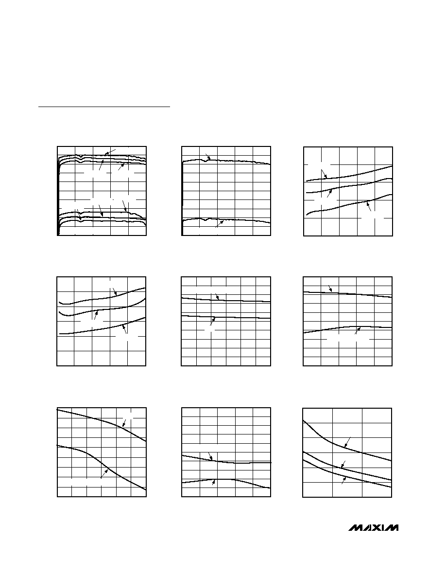
Typical Operating Characteristics
(MAX2130 EV kit, V
CC
= +5V, R
BIAS
= 15k
±1%, T
A
= +25∞C, unless otherwise noted.)
MAX2130
Broadband, Two-Output, Low-Noise
Amplifier for TV Tuner Applications
4
_______________________________________________________________________________________
Typical Operating Characteristics (continued)
(MAX2130 EV kit, V
CC
= +5V, R
BIAS
= 15k
±1%, T
A
= +25∞C, unless otherwise noted.)
7
10
9
8
11
12
13
14
15
16
17
0
400
200
600
800
1000
GAIN vs. FREQUENCY
R
BIAS
= 15k
MAX2130 toc04
FREQUENCY (MHz)
GAIN (dB)
LNA
LOOP-OUT AMPLIFIER
T
A
= -40
∞C
T
A
= +25
∞C
T
A
= +85
∞C
T
A
= -40
∞C
T
A
= +85
∞C
T
A
= +25
∞C
7
10
9
8
11
12
13
14
15
16
17
0
400
200
600
800
1000
GAIN vs. FREQUENCY
R
BIAS
= 25k
MAX2130 toc05
FREQUENCY (MHz)
GAIN (dB)
LOOP-OUT AMPLIFIER
LNA
0
1
3
2
4
5
0
400
200
600
800
1000
LNA NOISE FIGURE vs. FREQUENCY
MAX2130 toc06
FREQUENCY (MHz)
NOISE FIGURE (dB)
T
A
= +85
∞C
T
A
= +25
∞C
T
A
= -40
∞C
0
2
1
4
3
5
6
0
400
200
600
800
1000
LOOP-OUT AMPLIFIER
NOISE FIGURE vs. FREQUENCY
MAX2130 toc07
FREQUENCY (MHz)
NOISE FIGURE (dB)
T
A
= +25
∞C
T
A
= -40
∞C
T
A
= +85
∞C
0
1.5
1.0
0.5
2.0
2.5
3.0
3.5
4.0
4.5
5.0
10.0
15.0
12.5
17.5
20.0
22.5
25.0
NOISE FIGURE vs. R
BIAS
MAX2130 toc08
R
BIAS
(k
)
NOISE FIGURE (dB)
LNA
LOOP-OUT AMPLIFIER
-5
-2
-3
-4
-1
0
1
2
3
4
5
-40
10
-15
35
60
85
INPUT P1dB vs. TEMPERATURE
MAX2130 toc09
TEMPERATURE (
∞C)
INPUT P1dB (dBm)
LNA
LOOP-OUT AMPLIFIER
-5
-3
-4
0
-1
-2
3
2
1
4
10.0
15.0
12.5
17.5
20.0
22.5
25.0
INPUT P1dB vs. R
BIAS
MAX2130 toc10
R
BIAS
(k
)
INPUT P1dB (dBm)
LNA
LOOP-OUT AMPLIFIER
25
28
27
26
29
30
31
32
33
34
35
-40
10
-15
35
60
85
INPUT IP2 vs. TEMPERATURE
MAX2130 toc11
TEMPERATURE (
∞C)
INPUT IP2 (dBm)
LNA
LOOP-OUT AMPLIFIER
15
25
20
35
30
40
45
10
15
20
25
MAX2130 toc12
R
BIAS
(k
)
INPUT IP2 (dBm)
LNA
INPUT IP2 vs. R
BIAS
100MHz
600MHz
800MHz

MAX2130
Broadband, Two-Output, Low-Noise
Amplifier for TV Tuner Applications
_______________________________________________________________________________________
5
15.0
15.5
16.0
16.5
17.0
17.5
18.0
18.5
19.0
-40
-15
10
35
60
85
INPUT IP3 vs. TEMPERATURE
MAX2130-14
TEMPERATURE (
∞C)
INPUT IP3 (dBm)
LOOP-OUT AMPLIFIER
LNA
10
12
16
14
18
20
MAX2130 toc15
R
BIAS
(k
)
INPUT IP3 (dBm)
10
20
15
25
LNA
INPUT IP3 vs. R
BIAS
600MHz
800MHz
100MHz
10
12
16
14
18
20
MAX2130 toc16
R
BIAS
(k
)
INPUT IP3 (dBm)
10
20
15
25
LOOP-OUT AMPLIFIER
INPUT IP3 vs. R
BIAS
600MHz
800MHz
100MHz
-60
-40
-50
-20
-30
-10
0
0
400
200
600
800
1000
ISOLATION vs. FREQUENCY
MAX2130 toc17
FREQUENCY (MHz)
ISOLATION (dB)
OUT2 TO OUT1
OUT1 TO IN
OUT2 TO IN
0
15
5
25
20
35
30
40
0
400
200
600
800
1000
IN PORT
RETURN LOSS vs. FREQUENCY
MAX2130 toc18
FREQUENCY (MHz)
RETURN LOSS (dB)
10
Z
o
= 75
20
15
10
5
0
0
400
200
600
800
1000
OUT1 PORT
RETURN LOSS vs. FREQUENCY
MAX2130 toc19
FREQUENCY (MHz)
RETURN LOSS (dB)
Z
o
= 75
0
15
10
5
20
25
30
35
40
45
50
0
400
200
600
800
1000
OUT2 PORT
RETURN LOSS vs. FREQUENCY
MAX2130 toc20
FREQUENCY (MHz)
RETURN LOSS (dB)
Z
o
= 75
20
25
35
30
40
45
MAX2130 toc13
R
BIAS
(k
)
INPUT IP2 (dBm)
10
20
15
25
LOOP-OUT AMPLIFIER
INPUT IP2 vs. R
BIAS
100MHz
600MHz
800MHz
Typical Operating Characteristics (continued)
(MAX2130 EV kit, V
CC
= +5V, R
BIAS
= 15k
±1%, T
A
= +25∞C, unless otherwise noted.)