 | –≠–ª–µ–∫—Ç—Ä–æ–Ω–Ω—ã–π –∫–æ–º–ø–æ–Ω–µ–Ω—Ç: MAX2244 | –°–∫–∞—á–∞—Ç—å:  PDF PDF  ZIP ZIP |
General Description
The MAX2244/MAX2245/MAX2246 single-supply, low-
voltage power amplifiers (PAs) are designed for 20dBm
BluetoothTM Class 1 applications in the 2.4GHz to 2.5GHz
band. The MAX2244/MAX2245 deliver a peak output
power of 22dBm with greater than 20dB output-power
control range. The 22dBm output power compensates for
the filter loss between the PA and the antenna, allowing
20dBm to be delivered to the antenna. The MAX2246 pro-
vides a peak output power of 20dBm for a 30% reduction
in supply current.
The PAs integrate a power detector and closed-loop
power-control circuitry to provide nearly constant output
power over the full range of supply voltage, temperature,
and input power level. The voltage at the analog control
input precisely controls the output power level.
The MAX2244/MAX2245/MAX2246 feature a low-current
shutdown mode through a simple logic input. Internal cir-
cuitry automatically controls the ramp-up/down of the
output power level during turn-on and turn-off to meet
Bluetooth spurious emissions requirements.
The devices operate from a 3V to 3.6V single supply.
The MAX2244/MAX2246 have a power-control voltage
range of 0.5V to 2V, and the MAX2245 has a control
voltage range of 0.9V to 2.2V. The devices are pack-
aged in a miniature ultra chip-scale package (UCSPTM),
significantly reducing the required board area.
Applications
Bluetooth Class 1 Radios
802.11 FHSS/HomeRFTM Radios
2.4GHz Cordless Phones
Features
o 2.4GHz to 2.5GHz Operation
o Accurate Closed-Loop Output Power Control
Over Full Temperature, Supply, and Input Power
Range
o Convenient Analog Power-Control Interface
o 22dBm Peak Output Power (MAX2244/MAX2245)
o 20dBm Peak Output with 30% Reduced Supply
Current (MAX2246)
o Internal Bandwidth-Limited Power Ramping
o 50 Integrated Input Match
o 0.5µA Shutdown Supply Current
o Ultra Chip-Scale Package (1.56mm
1.56mm)
MAX2244/MAX2245/MAX2246
2.5GHz, 22dBm/20dBm Power Amplifiers with
Analog Closed-Loop Power Control
________________________________________________________________ Maxim Integrated Products
1
Ordering Information
19-2204; Rev 2; 8/03
For pricing, delivery, and ordering information, please contact Maxim/Dallas Direct! at
1-888-629-4642, or visit Maxim's website at www.maxim-ic.com.
PART
TEMP
RANGE
BUMP
PACKAGE
TOP
MARK
MAX2244EBL-T
-40
∞C to +85∞C
9 UCSP*-9
AAP
MAX2245EBL-T
-40
∞C to +85∞C
9 UCSP*-9
AAQ
MAX2246EBL-T
-40
∞C to +85∞C
9 UCSP*-9
AAY
*UCSP reliability is integrally linked to the user's assembly
methods, circuit board material, and environment. See the
UCSP Reliability Notice in the UCSP Reliability section of this
data sheet for more information.
Bluetooth is a trademark of Ericsson Corp.
UCSP is a trademark of Maxim Integrated Products, Inc.
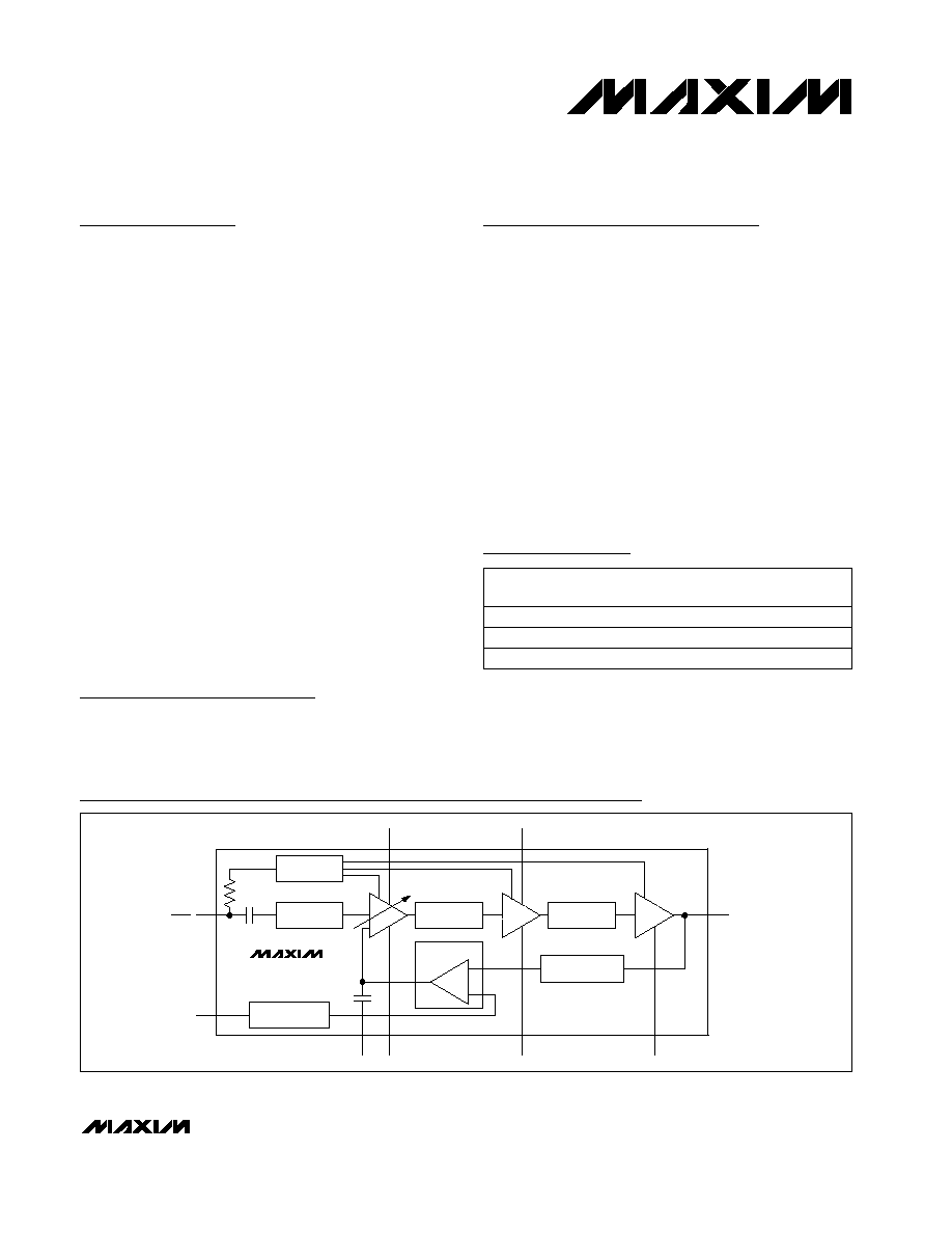
MATCH
MATCH
BIAS
SHUTDOWN
ANALOG
INTERFACE
MATCH
POWER
DETECTOR
C1
C3
B2
A3
B3
A2
C2
RFIN/
SHDN
PC
GND
GND
RFOUT
V
CC2
V
CC1
A1
B1
MAX2244
CONTROL
AMP
MAX2245
MAX2246
GND
GND
Functional Diagram
Pin Configuration appears at end of data sheet.
HomeRF is a trademark of The HomeRF Working Group.

MAX2244/MAX2245/MAX2246
2.5GHz, 22dBm/20dBm Power Amplifiers with
Analog Closed-Loop Power Control
2
_______________________________________________________________________________________
ABSOLUTE MAXIMUM RATINGS
DC ELECTRICAL CHARACTERISTICS
(Typical Application Circuit, V
CC
= 3V to 3.6V, no RF signals applied, V
SHDN
2V, V
PC
= 0, T
A
= -40∞C to +85∞C, unless otherwise
noted. Typical values are at V
CC
= 3V, T
A
= +25∞C, unless otherwise noted.) (Note 1)
Stresses beyond those listed under "Absolute Maximum Ratings" may cause permanent damage to the device. These are stress ratings only, and functional
operation of the device at these or any other conditions beyond those indicated in the operational sections of the specifications is not implied. Exposure to
absolute maximum rating conditions for extended periods may affect device reliability.
V
CC1
, V
CC2
, RFOUT to GND .................................-0.3V to +6.0V
RFIN/SHDN, PC to GND.............................-0.3V to (V
CC
+ 0.3V)
RF Input Power (RFIN)....................................................+10dBm
Load Mismatch (VSWR) Without Damage ..............................6:1
Continuous Power Dissipation (T
A
= +85∞C)
9-Pin UCSP (derate 8.8mW/∞C above T
A
= +85∞C).....700mW
Operating Temperature Range ...........................-40∞C to +85∞C
Junction Temperature .....................................................+150∞C
Storage Temperature Range .............................-65∞C to +150∞C
Continuous Operating Lifetime............10 years x 0.935
(T
A
- 65∞C)
(for operating temperature 65∞C < T
A
< 85∞C)
PARAMETER
CONDITIONS
MIN
TYP
MAX
UNITS
Supply Voltage
3.0
3.6
V
V
PC
= 0.5V, T
A
= +25
∞C
65
83
V
PC
= 0.5V, T
A
= -40
∞C to +85∞C
98
V
PC
= 2V, T
A
= +25
∞C
172
200
MAX2244
P
RF IN
= 0 to 4d Bm ,
2.45GH z
V
PC
= 2V, T
A
= -40
∞C to +85∞C
205
V
PC
= 0.9V, T
A
= +25
∞C
65
87
V
PC
= 0.9V, T
A
= -40
∞C to +85∞C
93
V
PC
= 2.2V, T
A
= +25
∞C
179
195
MAX2245
P
RF IN
= 0 to 4d Bm ,
2.45GH z
V
PC
= 2.2V, T
A
= -40
∞C to +85∞C
208
V
PC
= 0.5V, T
A
= +25
∞C
42
55
V
PC
= 0.5V, T
A
= -40
∞C to +85∞C
61
V
PC
= 2V, T
A
= +25
∞C
118
140
Supply Current (Note 2)
MAX2246
P
RFIN
= 0 to 4dBm,
2.45GHz
V
PC
= 2V, T
A
= -40
∞C to +85∞C
144
mA
Shutdown Supply Current
SHDN = GND
0.5
10
µA
SHDN Input Voltage High
2.0
V
SHDN Input Voltage Low
0.6
V
SHDN Input Current
-1
1
µA
MAX2244/MAX2246
0.5
2.0
PC Input Voltage Range
Active control range
MAX2245
0.9
2.5
V
MAX2244/MAX2246, V
PC
= 0 to 2.5V
-15
5
PC Input Current
MAX2245, V
PC
= 0 to 3V
-20
10
µA
CAUTION! ESD SENSITIVE DEVICE
MAX2244/MAX2245/MAX2246
2.5GHz, 22dBm/20dBm Power Amplifiers with
Analog Closed-Loop Power Control
_______________________________________________________________________________________
3
AC ELECTRICAL CHARACTERISTICS
(Typical Application Circuit, V
CC
= 3V, P
RFIN
= 0 to 4dBm, f
RFIN
= 2.45GHz, 50
system, V
SHDN
2V, T
A
= +25∞C, unless otherwise
noted. Typical values are at V
CC
= 3V, P
RFIN
= 2dBm, f
RFIN
= 2.45GHz, T
A
= +25∞C, unless otherwise noted.)
Note 1: Limits are 100% production tested at T
A
= +25∞C. Limits over the entire operating temperature range are guaranteed by
design and characterization, but are not production tested.
Note 2: Guaranteed by design and characterization.
Note 3: Assumes the output is optimally matched to cover the 2.4GHz to 2.5GHz band.
Note 4: Valid for the case in which the output stage is matched with a two-section transmission line, lowpass matching network to
minimize the 2nd and 3rd harmonics, as shown in the Typical Application Circuit.
Note 5: Output measured in a 100kHz RBW. Power on/off duty cycle = 50%. Test signal: GFSK, BT = 0.5, 1 bit/symbol, 1Mbps,
frequency deviation = 175kHz.
Note 6: The total turn-on and settling time required for the PA output power to settle to within ±1dB of the final value.
Note 7: The total turn-off time for the PA output power to drop to -10dBm.
PARAMETER
CONDITIONS
MIN
TYP
MAX
UNITS
Frequency Range (Note 3)
2.4
2.5
GHz
Input Power
0
4
dBm
MAX2244, V
PC
= 0.5V
T
A
= +25
∞C
0
4
7
T
A
= +25
∞C
20.5
22.0
23.5
MAX2244, V
PC
= 2V
T
A
= -40
∞C to +85∞C
20
24
MAX2245, V
PC
= 0.9V
T
A
= +25
∞C
0
4
7
T
A
= +25
∞C
20.5
22.0
23.5
MAX2245, V
PC
= 2.2V
T
A
= -40
∞C to +85∞C
20
24
MAX2246, V
PC
= 0.5V
T
A
= +25
∞C
-4.5
0.5
5.5
T
A
= +25
∞C
19
20
21
Output Power (Note 2)
MAX2246, V
PC
= 2V
T
A
= -40
∞C to +85∞C
17
21
dBm
MAX2244/MAX2245
-7
-1
Harmonic Output (Notes 2, 4)
P
RFOUT
at any level
MAX2246
-16
-13
dBm
Shutdown Mode Output (Note 2)
V
SHDN
0.6V, P
RFIN
= 4dBm
-30
dBm
Frequency offset =
±500kHz
-20
dBc
Frequency offset =
±1.5MHz
-20
In-Band Spurious (Notes 2, 3, 5)
Frequency offset = ±2.5MHz
-40
dBm
Nonharmonic Spurious Output
(Note 2)
All power levels, load VSWR
3:1
-30
dBm
MAX2244/MAX2246, V
PC
steps from 0 to 2V
4
Power Ramp Turn-On Time
(Notes 2, 6)
MAX2245/MAX2246, V
PC
steps from 0 to 2.5V
4
µs
MAX2244, V
PC
steps from 2V to 0
1.8
Power Ramp Turn-Off Time
(Notes 2, 7)
MAX2245, V
PC
steps from 2.5V to 0
1.8
µs
Input VSWR (Note 2)
R
S
= 50
, over full P
RFIN
range
1.5:1
2:1
MAX2244/MAX2245/MAX2246
2.5GHz, 22dBm/20dBm Power Amplifiers with
Analog Closed-Loop Power Control
4
_______________________________________________________________________________________
Typical Operating Characteristics
(Typical Application Circuit, V
CC
= 3V, P
RFIN
= 2dBm, f
RFIN
= 2.45GHz, SHDN = V
CC
, T
A
= +25∞C, unless otherwise noted.)
-20
-10
10
0
20
0
1.0
0.5
1.5
2.0
2.5
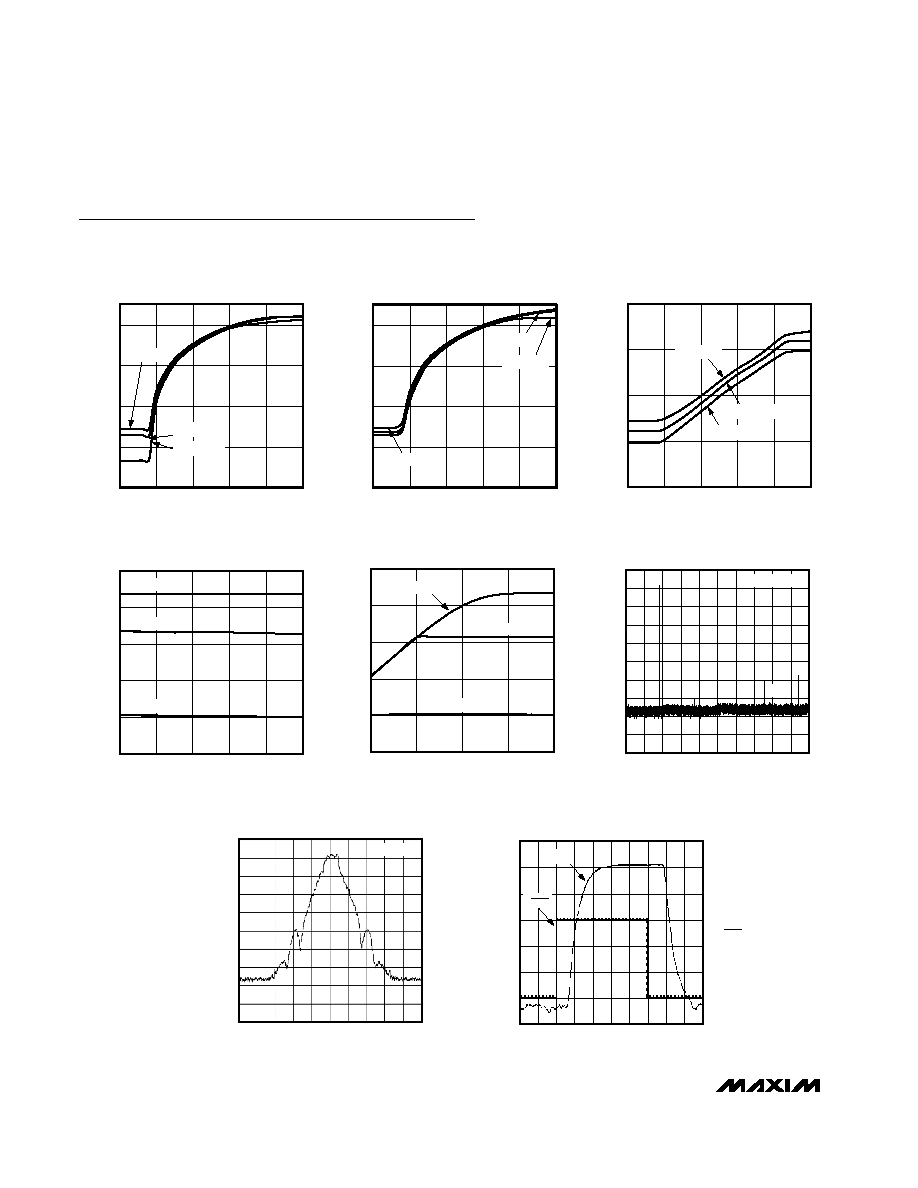
MAX2244
OUTPUT POWER vs. POWER CONTROL (V
PC
)
MAX2244-46 toc01
V
PC
(V)
OUTPUT POWER (dBm)
T
A
= +85
∞C
T
A
= +25
∞C
T
A
= -40
∞C
-20
-10
10
0
20
0
1.0
0.5
1.5
2.0
2.5
MAX2244
OUTPUT POWER vs. POWER CONTROL (V
PC
)
MAX2244-46 toc02
V
PC
(V)
OUTPUT POWER (dBm)
V
CC
= 5.0V
V
CC
= 3V
V
CC
= 4V
200
150
100
50
0
0
1.0
0.5
1.5
2.0
2.5
MAX2244 SUPPLY CURRENT
vs. POWER CONTROL (V
PC
)
MAX2244-46 toc03
V
PC
(V)
SUPPLY CURRENT (mA)
T
A
= +85
∞C
T
A
= +25
∞C
T
A
= -40
∞C
MAX2244
OUTPUT POWER vs. FREQUENCY
MAX2244-46 toc04
FREQUENCY (GHz)
OUTPUT POWER (dBm)
2.48
2.46
2.44
2.42
5
10
15
20
25
0
2.40
2.50
V
PC
= 0.5V
V
PC
= 1.0V
V
PC
= 2.0V
MAX2244
OUTPUT POWER vs. INPUT POWER
MAX2244-46 toc05
INPUT POWER (dBm)
OUTPUT POWER (dBm)
0
-5
-10
5
10
15
20
25
0
-15
5
V
PC
= 2V
V
PC
= 1V
V
PC
= 0.5V
MAX2244
HARMONIC OUTPUT SPECTRUM
MAX2244-46toc06
10dB/div
0.1
FREQUENCY (GHz)
13
0dBm
f
O
2f
O
3f
O
4f
O
5f
O
V
PC
= 2V
MAX2244
FSK MODULATED OUTPUT SPECTRUM
MAX2244-46 toc07
10dB/div
0dBm
V
PC
= 2V
2.45GHz
0.5MHz/div
MAX2244
POWER-ON/OFF CHARACTERISTICS
MAX2244-46 toc08
TIME (2
µs/div)
OUTPUT POWER (dBm)
-30
-20
-10
0
10
20
V
SHDN
(V)
0
1
2
3
4
5
30
-40
P
RFOUT
V
SHDN
Typical Operating Characteristics (continued)
(Typical Application Circuit, V
CC
= 3V, P
RFIN
= 2dBm, f
RFIN
= 2.45GHz, SHDN = V
CC
, T
A
= +25∞C, unless otherwise noted.)
MAX2244/MAX2245/MAX2246
2.5GHz, 22dBm/20dBm Power Amplifiers with
Analog Closed-Loop Power Control
_______________________________________________________________________________________
5
-20
0
-10
10
20
0
1.0
0.5
1.5
2.0
2.5
3.0
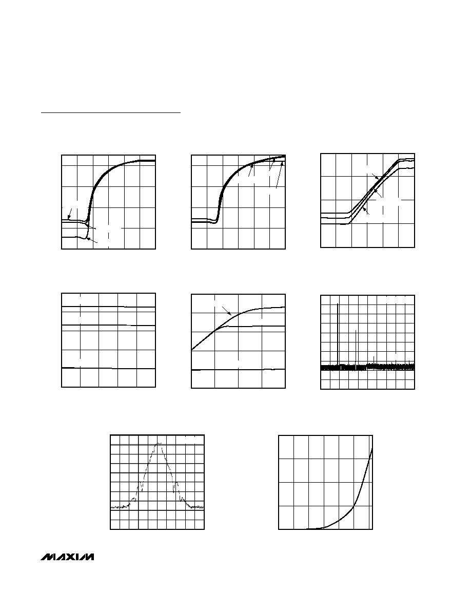
MAX2245
OUTPUT POWER vs. POWER CONTROL (V
PC
)
MAX2244-46 toc09
V
PC
(V)
OUTPUT POWER (dBm)
T
A
= +25
∞C
T
A
= -40
∞C
T
A
= +85
∞C
-20
-10
0
10
20
0
1.0
0.5
1.5
2.0
2.5
3.0
MAX2245
OUTPUT POWER vs. POWER CONTROL (V
PC
)
MAX2244-46 toc10
V
PC
(V)
OUTPUT POWER (dBm)
V
CC
= 3V
V
CC
= 4V
V
CC
= 5V
200
150
100
50
0
0
1.5
0.5
1.0
2.0
2.5
3.0
MAX2245
SUPPLY CURRENT vs. POWER CONTROL (V
PC
)
MAX2244-46 toc11
V
PC
(V)
SUPPLY CURRENT (mA)
T
A
= +25
∞C
T
A
= -40
∞C
T
A
= +85
∞C
MAX2245
OUTPUT POWER vs. FREQUENCY
MAX2244-46 toc12
FREQUENCY (GHz)
OUTPUT POWER (dBm)
2.48
2.46
2.44
2.42
5
10
15
20
25
0
2.40
2.50
V
PC
= 1V
V
PC
= 1.5V
V
PC
= 2.5V
MAX2245
OUTPUT POWER vs. INPUT POWER
MAX2244-46 toc13
INPUT POWER (dBm)
OUTPUT POWER (dBm)
0
-5
-10
5
10
15
20
25
0
-15
5
V
PC
= 2.5V
V
PC
= 1.5V
V
PC
= 1V
MAX2245
HARMONIC OUTPUT SPECTRUM
MAX2244/45 toc14
10dB/div
0dBm
0.1
FREQUENCY (GHz)
13
f
O
2f
O
3f
O
4f
O
5f
O
V
PC
= 2.2V
MAX2245
FSK MODULATED OUTPUT SPECTRUM
MAX2244-46 toc15
10dB/div
2.45GHz
0.5MHz/div
0dBm
V
PC
= 2.2V
SHUTDOWN CURRENT vs. TEMPERATURE
MAX2244-46 toc16
TEMPERATURE (
∞C)
SHUTDOWN CURRENT (nA)
80
60
40
20
0
-20
200
400
600
800
0
-40