
General Description
The MAX3070E≠MAX3079E 3.3V, ±15kV ESD-protected,
RS-485/RS-422 transceivers feature one driver and one
receiver. These devices include fail-safe circuitry, guar-
anteeing a logic-high receiver output when receiver
inputs are open or shorted. The receiver outputs a logic
high if all transmitters on a terminated bus are disabled
(high impedance). The MAX3070E≠MAX3079E include a
hot-swap capability to eliminate false transitions on the
bus during power-up or hot insertion.
The MAX3070E/MAX3071E/MAX3072E feature reduced
slew-rate drivers that minimize EMI and reduce reflec-
tions caused by improperly terminated cables, allowing
error-free data transmission up to 250kbps. The
MAX3073E/MAX3074E/MAX3075E also feature slew-
rate-limited drivers but allow transmit speeds up to
500kbps. The MAX3076E/MAX3077E/MAX3078E driver
slew rates are not limited, making transmit speeds up to
16Mbps possible. The MAX3079E slew rate is pin
selectable for 250kbps, 500kbps, and 16Mbps.
The MAX3072E/MAX3075E/MAX3078E are intended for
half-duplex communications, and the MAX3070E/
MAX3071E/MAX3073E/MAX3074E/MAX3076E/MAX307
7E are intended for full-duplex communications. The
MAX3079E is selectable for half-duplex or full-duplex
operation. It also features independently programmable
receiver and transmitter output phase through
separate pins.
The MAX3070E≠MAX3079E transceivers draw 800µA
of supply current when unloaded or when fully loaded
with the drivers disabled. All devices have a 1/8-unit
load receiver input impedance, allowing up to 256
transceivers on the bus.
Applications
Lighting Systems
Industrial Control
Telecom
Security Systems
Instrumentation
Features
o 3.3V Operation
o Electrostatic Discharge (ESD) Protection for
RS-485 I/O Pins
±15kV Human Body Model
o True Fail-Safe Receiver While Maintaining
EIA/TIA-485 Compatibility
o Hot-Swap Input Structure on DE and RE
o Enhanced Slew-Rate Limiting Facilitates Error-
Free Data Transmission
(MAX3070E≠MAX3075E/MAX3079E)
o Low-Current Shutdown Mode (Except
MAX3071E/MAX3074E/MAX3077E)
o Pin-Selectable Full-/Half-Duplex Operation
(MAX3079E)
o Phase Controls to Correct for Twisted-Pair
Reversal (MAX3079E)
o Allow Up to 256 Transceivers on the Bus
o Available in Industry-Standard 8-Pin SO Package
MAX3070E≠MAX3079E
+3.3V, ±15kV ESD-Protected, Fail-Safe,
Hot-Swap, RS-485/RS-422 Transceivers
________________________________________________________________ Maxim Integrated Products
1
Ordering Information
19-2668; Rev 1; 1/03
For pricing, delivery, and ordering information, please contact Maxim/Dallas Direct! at
1-888-629-4642, or visit Maxim's website at www.maxim-ic.com.
PART
TEMP RANGE
PIN-PACKAGE
MAX3070EEPD
-40∞C to +85∞C
14 Plastic DIP
MAX3070EESD
-40∞C to +85∞C
14 SO
MAX3070EAPD
-40∞C to +125∞C
14 Plastic DIP
MAX3070EASD
-40∞C to +125∞C
14 SO
MAX3071EEPA
-40∞C to +85∞C
8 Plastic DIP
MAX3071EESA
-40∞C to +85∞C
8 SO
MAX3071EAPA
-40∞C to +125∞C
8 Plastic DIP
MAX3071EASA
-40∞C to +125∞C
8 SO
Selector Guide, Pin Configurations, and Typical Operating
Circuits appear at end of data sheet.
Ordering Information continued at end of data sheet.
MAX3070E≠MAX3079E
+3.3V, ±15kV ESD-Protected, Fail-Safe,
Hot-Swap, RS-485/RS-422 Transceivers
2
_______________________________________________________________________________________
ABSOLUTE MAXIMUM RATINGS
DC ELECTRICAL CHARACTERISTICS
(V
CC
= 3.3V ±10%, T
A
=T
MIN
to T
MAX
, unless otherwise noted. Typical values are at V
CC
= 3.3V and T
A
= +25∞C.) (Note 1)
Stresses beyond those listed under "Absolute Maximum Ratings" may cause permanent damage to the device. These are stress ratings only, and functional
operation of the device at these or any other conditions beyond those indicated in the operational sections of the specifications is not implied. Exposure to
absolute maximum rating conditions for extended periods may affect device reliability.
(All voltages referenced to GND)
Supply Voltage (V
CC
).............................................................+6V
Control Input Voltage (RE, DE, SLR,
H/F, TXP, RXP)......................................................-0.3V to +6V
Driver Input Voltage (DI)...........................................-0.3V to +6V
Driver Output Voltage (Z, Y, A, B) .............................-8V to +13V
Receiver Input Voltage (A, B)....................................-8V to +13V
Receiver Input Voltage
Full Duplex (A, B) ..................................................-8V to +13V
Receiver Output Voltage (RO)....................-0.3V to (V
CC
+ 0.3V)
Driver Output Current .....................................................±250mA
Continuous Power Dissipation (T
A
= +70∞C)
8-Pin SO (derate 5.88mW/∞C above +70∞C) .................471mW
8-Pin Plastic DIP (derate 9.09mW/∞C above +70∞C) .....727mW
14-Pin SO (derate 8.33mW/∞C above +70∞C) ...............667mW
14-Pin Plastic DIP (derate 10.0mW/∞C above +70∞C) ...800mW
Operating Temperature Ranges
MAX307_EE_ _ ................................................-40∞C to +85∞C
MAX307_EA_ _ ..............................................-40∞C to +125∞C
Junction Temperature ......................................................+150∞C
Storage Temperature Range .............................-65∞C to +150∞C
Lead Temperature (soldering, 10s) .................................+300∞C
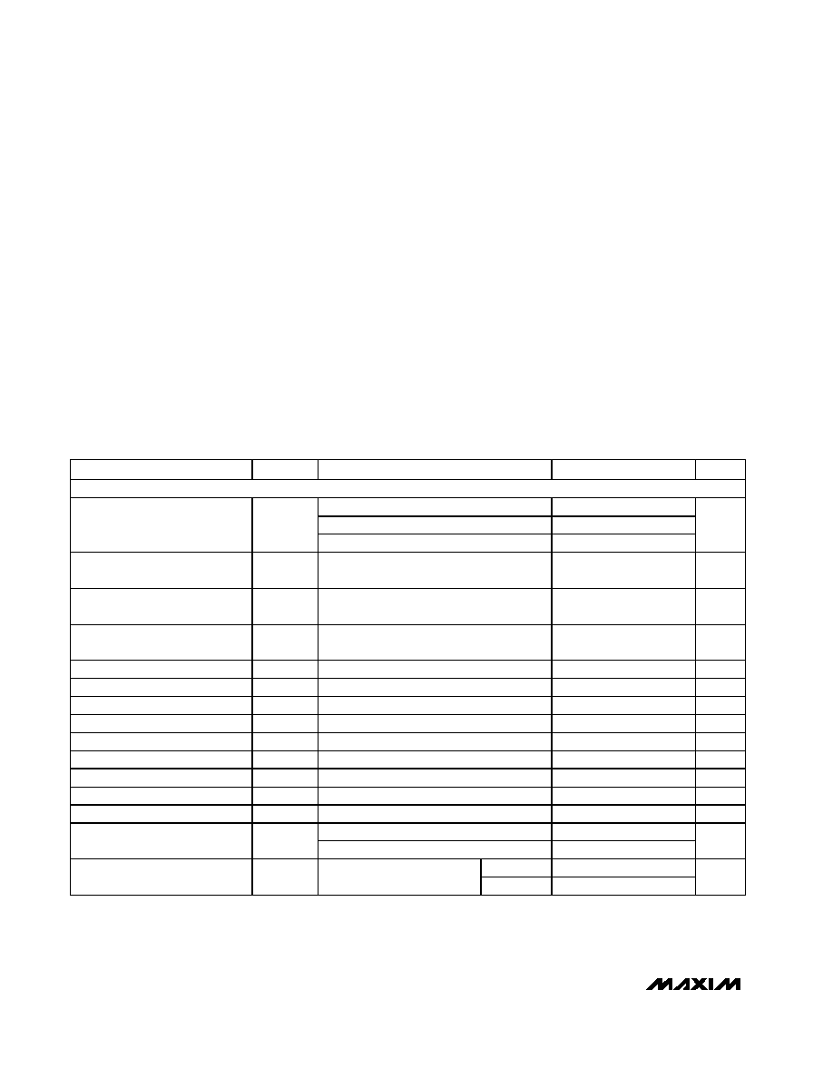
PARAMETER
SYMBOL
CONDITIONS
MIN
TYP
MAX
UNITS
DRIVER
R
L
= 100
(RS422), Figure 1
2
V
CC
R
L
= 54
(RS485), Figure 1
1.5
V
CC
Differential Driver Output
V
OD
No load
V
CC
V
Change in Magnitude of
Differential Output Voltage
V
OD
R
L
= 100
or 54, Figure 1 (Note 2)
0.2
V
Driver Common-Mode Output
Voltage
V
OC
R
L
= 100
or 54, Figure 1
V
CC
/ 2
3
V
Change in Magnitude of
Common-Mode Voltage
V
OC
R
L
= 100
or 54, Figure 1 (Note 2)
0.2
V
Input High Voltage
V
IH
DE, DI, RE, TXP, RXP, H/F
2
V
Input Low Voltage
V
IL
DE, DI, RE, TXP, RXP, H/F
0.8
V
Input Hysteresis
V
HYS
DE, DI, RE, TXP, RXP, H/F
100
mV
Input Current
I
IN1
DE, DI, RE
±1
µA
Input Impedance First Transition
DE
1
10
k
Input Current
I
IN2
TXP, RXP, H/F internal pulldown
10
40
µA
SRL Input High Voltage
V
CC
- 0.4
V
SRL Input Middle Voltage
V
CC
x 0.4 V
CC
x 0.6
V
SRL Input Low Voltage
0.4
V
SRL = V
CC
75
SRL Input Current
SRL = GND
-75
µA
V
IN
= +12V
125
Output Leakage (Y and Z)
Full Duplex
I
O
DE = GND,
V
CC
= GND or 3.6V
V
IN
= -7V
-100
µA

MAX3070E≠MAX3079E
+3.3V, ±15kV ESD-Protected, Fail-Safe,
Hot-Swap, RS-485/RS-422 Transceivers
_______________________________________________________________________________________
3
DC ELECTRICAL CHARACTERISTICS (continued)
(V
CC
= 3.3V ±10%, T
A
=T
MIN
to T
MAX
, unless otherwise noted. Typical values are at V
CC
= 3.3V and T
A
= +25∞C.) (Note 1)
PARAMETER
SYMBOL
CONDITIONS
MIN
TYP
MAX
UNITS
0
V
OUT
12V (Note 3)
40
250
Driver Short-Circuit Output
Current
I
OSD
-7V
V
OUT
V
CC
(Note 3)
-250
-40
mA
(V
CC
- 1V)
V
OUT
12V (Note 3)
20
Driver Short-Circuit Foldback
Output Current
I
OSDF
-7V
V
OUT
1V (Note 3)
-20
mA
Thermal-Shutdown Threshold
T
TS
175
∞C
Thermal-Shutdown Hysteresis
T
TSH
15
∞C
V
IN
= +12V
125
Input Current (A and B)
I
A, B
DE = GND,
V
CC
= GND or 3.6
V
IN
= -7V
-100
µA
RECEIVER
Receiver Differential Threshold
Voltage
V
TH
-7V
V
CM
12V
-200
-125
-50
mV
Receiver Input Hysteresis
V
TH
V
A
+ V
B
= 0V
15
mV
RO Output High Voltage
V
OH
I
O
= -1mA
V
CC
- 0.6
V
RO Output Low Voltage
V
OL
I
O
= 1mA
0.4
V
Three-State Output Current at
Receiver
I
OZR
0
V
O
V
CC
± 1
µA
Receiver Input Resistance
R
IN
-7V
V
CM
12V
96
k
Receiver Output Short-Circuit
Current
I
OSR
0V
V
RO
V
CC
±80
mA
SUPPLY CURRENT
No load, RE = 0, DE = V
CC
0.8
1.5
No load, RE = V
CC
, DE = V
CC
0.8
1.5
Supply Current
I
CC
No load, RE = 0, DE = 0
0.8
1.5
mA
Supply Current in Shutdown
Mode
I
SHDN
RE = V
CC
, DE = GND
0.05
10
µA
ESD PROTECTION
ESD Protection for Y, Z, A, and B
Human Body Model
±15
kV
Note 1: All currents into the device are positive. All currents out of the device are negative. All voltages are referred to device
ground, unless otherwise noted.
Note 2:
V
OD
and
V
OC
are the changes in V
OD
and V
OC
, respectively, when the DI input changes state.
Note 3: The short-circuit output current applies to peak current just prior to foldback current limiting. The short-circuit foldback out-
put current applies during current limiting to allow a recovery from bus contention.

MAX3070E≠MAX3079E
+3.3V, ±15kV ESD-Protected, Fail-Safe,
Hot-Swap, RS-485/RS-422 Transceivers
4
_______________________________________________________________________________________
DRIVER SWITCHING CHARACTERISTICS
MAX3070E/MAX3071E/MAX3072E/MAX3079E with SRL = UNCONNECTED (250kbps)
(V
CC
= 3.3V ±10%, T
A
= T
MIN
to T
MAX
, unless otherwise noted. Typical values are at V
CC
= 3.3V and T
A
= +25∞C.)
PARAMETER
SYMBOL
CONDITIONS
MIN
TYP
MAX
UNITS
t
DPLH
250
1500
Driver Propagation Delay
t
DPHL
C
L
= 50pF, R
L
= 54
, Figures 2 and 3
250
1500
ns
Driver Differential Output Rise or
Fall Time
t
DR ,
t
DF
C
L
= 50pF, R
L
= 54
, Figures 2 and 3
350
1600
ns
Differential Driver Output Skew
|t
DPLH
- t
DPHL
|
t
DSKEW
C
L
= 50pF, R
L
= 54
, Figures 2 and 3
200
ns
Maximum Data Rate
250
kbps
Driver Enable to Output High
t
DZH
Figure 4
2500
ns
Driver Enable to Output Low
t
DZL
Figure 5
2500
ns
Driver Disable Time from Low
t
DLZ
Figure 5
100
ns
Driver Disable Time from High
t
DHZ
Figure 4
100
ns
Driver Enable from Shutdown to
Output High
t
DZH(SHDN)
Figure 4
5500
ns
Driver Enable from Shutdown to
Output Low
t
DZL(SHDN)
Figure 5
5500
ns
Time to Shutdown
t
SHDN
50
200
600
ns
RECEIVER SWITCHING CHARACTERISTICS
MAX3070E/MAX3071E/MAX3072E/MAX3079E with SRL = UNCONNECTED (250kbps)
(V
CC
= 3.3V ±10%, T
A
= T
MIN
to T
MAX
, unless otherwise noted. Typical values are at V
CC
= 3.3V and T
A
= +25∞C.)
PARAMETER
SYMBOL
CONDITIONS
MIN
TYP
MAX
UNITS
t
RPLH
200
Receiver Propagation Delay
t
RPHL
C
L
= 15pF, Figures 6 and 7
200
ns
Receiver Output Skew
|t
RPLH
- t
RPHL
|
t
RSKEW
C
L
= 15pF, Figures 6 and 7
30
ns
Maximum Data Rate
250
kbps
Receiver Enable to Output Low
t
RZL
Figure 8
50
ns
Receiver Enable to Output High
t
RZH
Figure 8
50
ns
Receiver Disable Time from Low
t
RLZ
Figure 8
50
ns
Receiver Disable Time from High
t
RHZ
Figure 8
50
ns
Receiver Enable from Shutdown
to Output High
t
RZH(SHDN)
Figure 8
4000
ns
Receiver Enable from Shutdown
to Output Low
t
RZL(SHDN)
Figure 8
4000
ns
Time to Shutdown
t
SHDN
50
200
600
ns

MAX3070E≠MAX3079E
+3.3V, ±15kV ESD-Protected, Fail-Safe,
Hot-Swap, RS-485/RS-422 Transceivers
_______________________________________________________________________________________
5
DRIVER SWITCHING CHARACTERISTICS
MAX3073E/MAX3074E/MAX3075E/MAX3079E with SRL = V
CC
(500kbps)
(V
CC
= 3.3V ±10%, T
A
= T
MIN
to T
MAX
, unless otherwise noted. Typical values are at V
CC
= 3.3V and T
A
= +25∞C.)
PARAMETER
SYMBOL
CONDITIONS
MIN
TYP
MAX
UNITS
t
DPLH
180
800
Driver Propagation Delay
t
DPHL
C
L
= 50pF, R
L
= 54
, Figures 2 and 3
180
800
ns
Driver Differential Output Rise or
Fall Time
t
DR ,
t
DF
C
L
= 50pF, R
L
= 54
, Figures 2 and 3
200
800
ns
Differential Driver Output Skew
|t
DPLH
- t
DPHL
|
t
DSKEW
C
L
= 50pF, R
L
= 54
, Figures 2 and 3
100
ns
Maximum Data Rate
500
kbps
Driver Enable to Output High
t
DZH
Figure 4
2500
ns
Driver Enable to Output Low
t
DZL
Figure 5
2500
ns
Driver Disable Time from Low
t
DLZ
Figure 5
100
ns
Driver Disable Time from High
t
DHZ
Figure 4
100
ns
Driver Enable from Shutdown to
Output High
t
DZH(SHDN)
Figure 4
4500
ns
Driver Enable from Shutdown to
Output Low
t
DZL(SHDN)
Figure 5
4500
ns
Time to Shutdown
t
SHDN
50
200
600
ns
RECEIVER SWITCHING CHARACTERISTICS
MAX3073E/MAX3074E/MAX3075E/MAX3079E with SRL = V
CC
(500kbps)
(V
CC
= 3.3V ±10%, T
A
= T
MIN
to T
MAX
, unless otherwise noted. Typical values are at V
CC
= 3.3V and T
A
= +25∞C.)
PARAMETER
SYMBOL
CONDITIONS
MIN
TYP
MAX
UNITS
t
RPLH
200
Receiver Propagation Delay
t
RPHL
C
L
= 15pF, Figures 6 and 7
200
ns
Receiver Output Skew
|t
RPLH
- t
RPHL
|
t
RSKEW
C
L
= 15pF, Figures 6 and 7
30
ns
Maximum Data Rate
500
kbps
Receiver Enable to Output Low
t
RZL
Figure 8
50
ns
Receiver Enable to Output High
t
RZH
Figure 8
50
ns
Receiver Disable Time from Low
t
RLZ
Figure 8
50
ns
Receiver Disable Time from High
t
RHZ
Figure 8
50
ns
Receiver Enable from Shutdown
to Output High
t
RZH(SHDN)
Figure 8
4000
ns
Receiver Enable from Shutdown
to Output Low
t
RZL(SHDN)
Figure 8
4000
ns
Time to Shutdown
t
SHDN
50
200
600
ns