 | –≠–ª–µ–∫—Ç—Ä–æ–Ω–Ω—ã–π –∫–æ–º–ø–æ–Ω–µ–Ω—Ç: MAX313CPE | –°–∫–∞—á–∞—Ç—å:  PDF PDF  ZIP ZIP |

For free samples & the latest literature: http://www.maxim-ic.com, or phone 1-800-998-8800.
For small orders, phone 1-800-835-8769.
_______________General Description
Maxim's MAX312/MAX313/MAX314 analog switches
feature low on-resistance (10
max) and 1.5
on-resis-
tance matching between channels. These switches con-
duct equally well in either direction. They offer low
leakage over temperature (2.5nA at +85∞C). Low power
consumption and ESD tolerance greater than 2000V per
Method 3015.7 are guaranteed.
The MAX312/MAX313/MAX314 are quad, single-
pole/single-throw (SPST) analog switches. The MAX312
is normally closed (NC), and the MAX313 is normally
open (NO). The MAX314 has two NC switches and two
NO switches. All three devices operate from a single
supply of +4.5V to +30V or from dual supplies of ±4.5V
to ±20V.
________________________Applications
Test Equipment
Communication Systems
PBX, PABX Systems
Audio Signal Routing
Avionics
Sample-and-Hold Circuits
Data Acquisition Systems
____________________________Features
o
Pin Compatible with DG411/DG412/DG413
o
Low On-Resistance (6.5
typical)
o
Guaranteed R
ON
Match Between Channels (1.5
max)
o
Guaranteed R
ON
Flatness over Specified Signal
Range (2
max)
o
Guaranteed ESD Protection > 2000V per Method
3015.7
o
Crosstalk > 96dB at 20kHz
o
Single-Supply Operation: +4.5V to +30V
Dual-Supply Operation: ±4.5V to ±20V
o
Rail-to-Rail Signal Handling
MAX312/MAX313/MAX314
10
, Quad, SPST, CMOS Analog Switches
________________________________________________________________
Maxim Integrated Products
1
SWITCHES SHOWN FOR LOGIC "0" INPUT
MAX313
LOGIC
SWITCH
0
1
OFF
ON
TOP VIEW
DIP/SO/TSSOP
SO/MAX312
LOGIC
SWITCH
0
1
ON
OFF
MAX314
LOGIC
SWITCHES
1, 4
0
1
OFF
ON
SWITCHES
2, 3
ON
OFF
16
15
14
13
12
11
10
9
1
2
3
4
5
6
7
8
IN2
COM2
NC2
V+
V-
NO1
COM1
IN1
MAX314
VL
NC3
COM3
IN3
IN4
COM4
NO4
GND
16
15
14
13
12
11
10
9
1
2
3
4
5
6
7
8
IN2
COM2
NC2
V+
V-
NC1
COM1
IN1
MAX312
VL
NC3
COM3
IN3
IN4
COM4
NC4
GND
16
15
14
13
12
11
10
9
1
2
3
4
5
6
7
8
IN2
COM2
NO2
V+
V-
NO1
COM1
IN1
MAX313
VL
NO3
COM3
IN3
IN4
COM4
NO4
GND
DIP/SO/TSSOP
DIP/SO/TSSOP
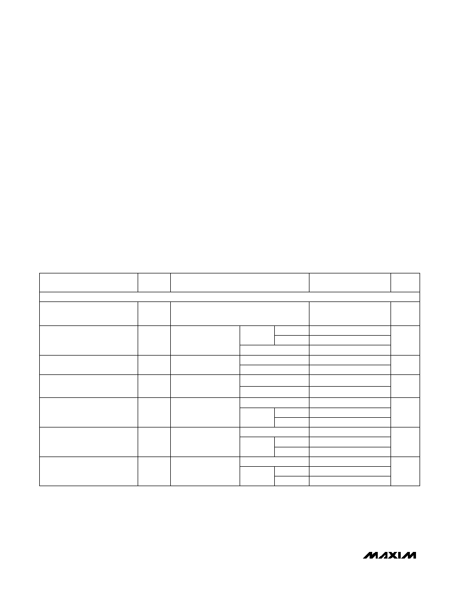
_____________________Pin Configurations/Functional Diagrams/Truth Tables
PART
MAX312
CPE
MAX312CSE
MAX312C/D
0∞C to +70∞C
0∞C to +70∞C
0∞C to +70∞C
TEMP. RANGE
PIN-PACKAGE
16 Plastic DIP
16 Narrow SO
Dice*
19-0420; Rev 1; 6/99
______________Ordering Information
Ordering Information continued at end of data sheet.
* Contact factory for dice specifications.
**Contact factory for availability.
MAX312EPE
MAX312ESE
-40∞C to +85∞C
-40∞C to +85∞C
16 Plastic DIP
16 Narrow SO
MAX312MJE
-55∞C to +125∞C
16 CERDIP**
MAX312CUE
0∞C to +70∞C
16 TSSOP
MAX312EUE
-40∞C to +85∞C
16 TSSOP
MAX312/MAX313/MAX314
10
, Quad, SPST, CMOS Analog Switches
2
_______________________________________________________________________________________
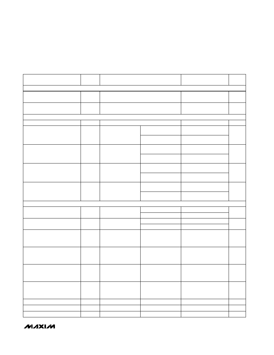
ABSOLUTE MAXIMUM RATINGS
ELECTRICAL CHARACTERISTICS--Dual Supplies
(V+ = 15V, V- = -15V, VL = 5V, GND = 0V, V
INH
= 2.4V, V
INL
= 0.8V, T
A
= T
MIN
to T
MAX
, unless otherwise noted.)
Stresses beyond those listed under "Absolute Maximum Ratings" may cause permanent damage to the device. These are stress ratings only, and functional
operation of the device at these or any other conditions beyond those indicated in the operational sections of the specifications is not implied. Exposure to
absolute maximum rating conditions for extended periods may affect device reliability.
Voltages Referenced to GND
V+ ...........................................................................-0.3V to +44V
V- ............................................................................+0.3V to -44V
V+ to V-...................................................................-0.3V to +44V
VL .....................................................(GND - 0.3V) to (V+ + 0.3V)
All Other Pins (Note 1) ................................(V- - 2V) to (V+ + 2V)
or 30mA (whichever occurs first)
Continuous Current (COM_, NO_, NC_).........................±100mA
Peak Current (COM_, NO_, NC_) ...................................±300mA
Continuous Power Dissipation (T
A
= +70∞C)
Plastic DIP (derate 10.53mW/∞C above +70∞C) ..........842mW
Narrow SO (derate 8.70mW/∞C above +70∞C) ............696mW
CERDIP (derate 10.00mW/∞C above +70∞C) ...............800mW
TSSOP (derate 6.7mW/∞C above +70∞C) ....................457mW
Operating Temperature Ranges
MAX31_C_ ..........................................................0∞C to +70∞C
MAX31_E_ .......................................................-40∞C to +85∞C
MAX31_M_.....................................................-55∞C to +125∞C
Storage Temperature Range .............................-65∞C to +150∞C
Lead Temperature (soldering, 10sec) .............................+300∞C
Note 1:
Signals on NC_, NO_, COM_, or IN_ exceeding V+ or V- will be clamped by internal diodes. Limit forward diode current to
maximum current rating.
(Note 3)
V
COM
= 10V,
V
NO
_ or V
NC
_ = ±10V
I
COM
= 10mA,
V
NO
_ or V
NC
_ = ±10V
I
COM
= 10mA,
V
NO
_ or V
NC
_ = ±10V
CONDITIONS
6.5
10
V
V-
V+
V
COM
_,
V
NO
_,
V
NC
_
Analog Signal Range
nA
-40
40
I
NO
I
NC
Off Leakage Current
(NO_ or NC_)
(Note 6)
-2.5
2.5
-0.5
-0.02
0.5
9
15
R
ON
On-Resistance
0.3
1.5
3
R
ON
On-Resistance Match Between
Channels (Note 4)
UNITS
MIN
TYP
MAX
(Note 2)
SYMBOL
PARAMETER
C, E
M
T
A
=
+25∞C
T
A
= T
MIN
to T
MAX
T
A
= +25∞C
T
A
= T
MIN
to T
MAX
T
A
= +25∞C
T
A
= T
MIN
to T
MAX
I
COM
= 10mA,
V
NO
_ or V
NC
_ = -5V,
0V, 5V
0.2
2
4
R
FLAT(ON)
On-Resistance Flatness
(Note 5)
T
A
= +25∞C
T
A
= T
MIN
to T
MAX
C, E
M
V
COM
= ±10V,
V
NO
_ or V
NC
_ = 10V
T
A
= +25∞C
T
A
= T
MIN
to T
MAX
C, E
M
nA
-40
40
I
NC(OFF)
COM Off Leakage Current
(Note 6)
-2.5
2.5
-0.5
-0.02
0.5
V
COM
= ±10V,
V
NO
_ or V
NC
_ = ±10V
T
A
= +25∞C
T
A
= T
MIN
to T
MAX
C, E
M
nA
-100
100
I
COM(ON)
COM On Leakage Current
(Note 6)
-5
5
-1
-0.04
1
ANALOG SWITCH
±
±
MAX312/MAX313/MAX314
10
, Quad, SPST, CMOS Analog Switches
_______________________________________________________________________________________
3
ELECTRICAL CHARACTERISTICS--Dual Supplies (continued)
(V+ = 15V, V- = -15V, VL = 5V, GND = 0V, V
INH
= 2.4V, V
INL
= 0.8V, T
A
= T
MIN
to T
MAX
, unless otherwise noted.)
IN_ = 2.4V, all others = 0.8V
CONDITIONS
-1
0.0001
1
µA
-0.500
0.005
0.500
I
INH
Input Current with Input Voltage
High
-5
5
µA
I+
UNITS
MIN
TYP
MAX
(Note 2)
SYMBOL
PARAMETER
T
A
= +25∞C
T
A
= T
MIN
to T
MAX
IN_ = 0.8V, all others = 2.4V
µA
-0.500
0.005
0.500
I
INL
Input Current with Input Voltage
Low
V
±4.5
±20.0
Power-Supply Range
Positive Supply Current
All channels on or off,
V
IN
= 0V or 5V,
V+ = 16.5V
V- = -16.5V
All channels on or off,
V
IN
= 0V or 5V,
V+ = 16.5V
V- = -16.5V
Negative Supply Current
-1
0.0001
1
-5
5
µA
I-
T
A
= +25∞C
T
A
= T
MIN
to T
MAX
All channels on or off,
V
IN
= 0V or 5V,
V+ = 16.5V
V- = -16.5V
Ground Current
-1
-0.0001
1
-5
5
µA
I
GND
T
A
= +25∞C
T
A
= T
MIN
to T
MAX
All channels on or off,
V
IN
= 0V or 5V,
V+ = 16.5V
V- = -16.5V
Logic Supply Current
-1
0.0001
1
-5
5
µA
I
L
T
A
= +25∞C
T
A
= T
MIN
to T
MAX
70
225
T
A
= +25∞C
MAX314 only, Figure 3,
R
L
= 300
,
C
L
= 35pF
t
D
Break-Before-Make Time Delay
ns
Figure 2,
V
COM
= ±10V
1
5
T
A
= +25∞C
t
ON
Turn-On Time
ns
275
T
A
= T
MIN
to T
MAX
65
185
T
A
= +25∞C
Figure 2,
V
COM
= ±10V
t
OFF
Turn-Off Time
ns
235
T
A
= T
MIN
to T
MAX
R
L
= 50
,
C
L
= 5pF,
f = 1MHz, Figure 6
V
CT
Crosstalk (Note 8)
dB
-85
T
A
= +25∞C
C
L
= 1.0nF
V
GEN
= 0V,
R
GEN
= 0
, Figure 4
V
CTE
Charge Injection
(Note 3)
pC
-30
20
30
T
A
= +25∞C
R
L
= 50
,
C
L
= 5pF,
f = 1MHz, Figure 5
V
ISO
Off Isolation (Note 7)
dB
-65
T
A
= +25∞C
f = 1MHz, Figure 7
C
(OFF)
NC or NO Capacitance
pF
15
T
A
= +25∞C
f = 1MHz, Figure 7
C
(COM)
COM Off Capacitance
pF
15
T
A
= +25∞C
f = 1MHz, Figure 7
C
(COM)
On Capacitance
pF
47
T
A
= +25∞C
LOGIC INPUT
POWER SUPPLY
DYNAMIC
MAX312/MAX313/MAX314
10
, Quad, SPST, CMOS Analog Switches
4
_______________________________________________________________________________________
ELECTRICAL CHARACTERISTICS--Single Supply
(V+ = 12V, V- = 0V, VL = 5V, GND = 0V, V
INH
= 2.4V, V
INL
= 0.8V, T
A
= T
MIN
to T
MAX
, unless otherwise noted.)
Note 2:
The algebraic convention, where the most negative value is a minimum and the most positive value a maximum, is used in
this data sheet.
Note 3:
Guaranteed by design.
Note 4:
R
ON
=
R
ON
max -
R
ON
min.
Note 5:
Flatness is defined as the difference between the maximum and minimum value of on-resistance as measured over the
specified analog signal range.
Note 6:
Leakage parameters are 100% tested at maximum-rated hot temperature and guaranteed by correlation at +25∞C.
Note 7:
Off isolation = 20log
10
[V
COM
/ (V
NC
or V
NO
)], V
COM
= output, V
NC
or V
NO
= input to off switch.
Note 8:
Between any two switches.
Note 9:
Leakage testing at single supply is guaranteed by testing with dual supplies.
(Note 3)
CONDITIONS
V
0
V+
V
COM
_,
V
NO
_,
V
NC
_
Analog Signal Range
UNITS
MIN
TYP
MAX
(Note 2)
SYMBOL
PARAMETER
12.5
25
I
COM
= 10mA,
V
NC
_ or V
NO
_ +10V
R
ON
Channel On-Resistance
35
-1
0.0001
1
T
A
= +25∞C
T
A
= T
MIN
to T
MAX
100
325
Figure 2,
V
NO
_ or V
NC
_ = 8V
ns
425
t
ON
Turn-On Time
(Note 3)
MAX314 only, Figure 3
R
L
= 300
,
C
L
= 35pF
t
D
Break-Before-Make Time Delay
(Note 3)
5
ns
I+
Positive Supply Current
-5
5
µA
T
A
= +25∞C
T
A
= T
MAX
V+ = 13.2V
all channels on or off,
V
IN
= 0V or 5V
-1
0.0001
1
V
L
= 5.5V
all channels on or off,
V
IN
= 0V or 5V
I
L
Logic Supply Current
-5
5
µA
T
A
= +25∞C
T
A
= T
MAX
-1
-0.0001
1
V
L
= 5.5V
all channels on or off,
V
IN
= 0V or 5V
I
GND
Ground Current
-5
5
µA
T
A
= +25∞C
T
A
= T
MAX
Figure 4,
C
L
= 1.0nF,
V
GEN
= 0V,
R
GEN
= 0V
V
CTE
Charge Injection
(Note 3)
-5
pC
T
A
= +25∞C
T
A
= T
MIN
to T
MAX
T
A
= +25∞C
T
A
= T
MIN
to T
MAX
95
175
Figure 2,
V
NO
_ or V
NC
_ = 8V
ns
225
t
OFF
Turn-Off Time
(Note 3)
T
A
= +25∞C
T
A
= +25∞C
ANALOG SWITCH
POWER SUPPLY
DYNAMIC

MAX312/MAX313/MAX314
10
, Quad, SPST, CMOS Analog Switches
_______________________________________________________________________________________
5
11
-15
-10
-5
10
5
ON-RESISTANCE vs. V
COM
(BIPOLAR SUPPLIES)
5
9
MAX312-01
V
COM
(V)
R
ON
(
)
0
15
7
15
19
17
13
A
B
C
A: V+, V- = ±5V,
B: V+, V- = ±10V,
C: V+, V- = ±15V
8
-15
-10
-5
10
5
ON-RESISTANCE vs. V
COM
AND
TEMPERATURE
2
6
MAX312-02
V
COM
(V)
R
ON
(
)
0
15
4
12
16
14
10
V+ = 15V,
V+ = -15V
A: T
A
= +125∞C
B: T
A
= +85∞C
C: T
A
= +70∞C
D: T
A
= +25∞C
E: T
A
= -55∞C
E
C
D
A
B
1000
1
0 1
3
5
15
ON-RESISTANCE vs. V
COM
(SINGLE SUPPLY, V- = 0V)
10
100
MAX312-03
V
COM
(V)
R
ON
(
)
2
4
11
13
12
14
6
8
10
7
9
A: V+ = 2.7V
B: V+ = 3.3V
C: V+ = 5V
D: V+ = 9V
E: V+ = 12V
F: V+ = 15V
E
F
C
D
A
B
8
0
2
4
10
8
ON-RESISTANCE vs. V
COM
AND
TEMPERATURE
2
6
MAX312-04
V
COM
(V)
R
ON
(
)
6
12
1
3
9
7
5
11
4
12
16
14
10
18
22
24
20
V+ = 12V,
V- = 0V
A: T
A
= +125∞C
B: T
A
= +85∞C
C: T
A
= +70∞C
D: T
A
= +25∞C
E: T
A
= -55∞C
E
C
D
A
B
-12
-8
4
0
CHARGE INJECTION
vs. V
COM
-40
-30
MAX312-07
V
COM
(V)
V
CTE
(pc)
-4
8 10 12 14
-14
-10
2
-2
-6
6
-10
0
20
10
-20
40
30
A: V+ = 15V, V- = -15V
B: V+ = 12V, V- = 0V
A
B
100
10
0.0001
-50
125
OFF LEAKAGE CURRENT
vs. TEMPERATURE
1
MAX312 TOC05
TEMPERATURE (
∞
C)
OFF LEAKAGE (nA)
25
0.01
0.001
-25
0
75
0.1
50
100
V+ = 15V,
V- = -15V,
V
NC
OR V
NO
= ±10V
V
COM
= 10V
±
100
10
0.0001
-50
125
ON LEAKAGE CURRENT
vs. TEMPERATURE
1
MAX312 TOC06
TEMPERATURE (
∞
C)
ON LEAKAGE (nA)
25
0.01
0.001
-25
0
75
0.1
50
100
V+ = 15V,
V- = -15V,
V
COM
= 10V
±
100
10
0.0001
-50
-75
125
1
MAX312 TOC08
TEMPERATURE (
∞
C)
I+, I-, I
L
(
µ
A)
25
0.01
0.001
-25
0
75
0.1
50
100
A: I+ = 16.5V
B: I- = -16.5V
C: I
L
= 5.5V
C
A
B
SUPPLY CURRENT
vs. TEMPERATURE
__________________________________________Typical Operating Characteristics
(T
A
= +25∞C, unless otherwise noted.)