 | –≠–ª–µ–∫—Ç—Ä–æ–Ω–Ω—ã–π –∫–æ–º–ø–æ–Ω–µ–Ω—Ç: MAX319 | –°–∫–∞—á–∞—Ç—å:  PDF PDF  ZIP ZIP |

_______________General Description
The MAX317/MAX318/MAX319 are precision, CMOS,
monolithic analog switches. The single-pole single-
throw (SPST) MAX317 is normally closed (NC), the
SPST MAX318 is normally open (NO), and the single-
pole double-throw (SPDT) MAX319 has one normally
open and one normally closed switch. All three parts
offer low on resistance (less than 35
), guaranteed to
match within 2
between channels and to remain flat
over the analog signal range (
3
max). They also
offer low leakage (less than 250pA at +25∞C and less
than 6nA at +85∞C) and fast switching (turn-on time
less than 175ns and turn-off time less than 145ns).
The MAX317/MAX318/MAX319 are fabricated with
Maxim's new improved silicon-gate process. Design
improvements guarantee extremely low charge injec-
tion (10pC), low power consumption (35µW), and elec-
trostatic discharge (ESD) greater than ±2000V. The
44V maximum breakdown voltage allows rail-to-rail ana-
log signal handling capability.
________________________Applications
Sample-and-Hold Circuits
Guidance and Control Systems
Heads-Up Displays
Test Equipment
Military Radios
Communications Systems
Battery-Powered Systems
PBX, PABX
____________________________Features
o
Low On Resistance <20
Typical (35
Max)
o
Guaranteed Matched On Resistance Between
Channels <2
o
Guaranteed Flat On Resistance over Analog
Signal Range
3
Max
o
Guaranteed Charge Injection <10pC
o
Guaranteed Off-Channel Leakage <6nA at +85∞C
o
ESD Guaranteed > 2000V per Method 3015.7
o
Single-Supply Operation (+10V to +30V)
Bipolar-Supply Operation (±4.5V to ±20V)
o
TTL-/CMOS-Logic Compatible
o
Rail-to-Rail Analog Signal Handling Capability
______________Ordering Information
MAX317/MAX318/MAX319
Precision, CMOS Analog Switches
_______________________________________________________________________
Maxim Integrated Products
1
Call toll free 1-800-998-8800 for free samples or literature.
19-0185; Rev 1; 11/94
Ordering Information continued on last page.
* Contact factory for dice specifications.
_____________________Pin Configurations/Functional Diagrams/Truth Tables
TOP VIEW
1
2
3
4
8
7
6
5
NO
V-
IN
VL
V+
GND
N.C.
COM
MAX318
DIP/SO
1
2
3
4
8
7
6
5
NC
V-
IN
VL
V+
GND
N.C.
COM
MAX317
DIP/SO
1
2
3
4
8
7
6
5
NO
V-
IN
VL
V+
GND
NC
COM
MAX319
DIP/SO
LOGIC
SWITCH
0
1
ON
OFF
SWITCHES SHOWN FOR LOGIC "0" INPUT
LOGIC
SWITCH
0
1
OFF
ON
LOGIC
NC
0
1
ON
OFF
NO
OFF
ON
MAX317
MAX318
MAX319
N.C. = No Connect
NC = Normally Closed
PART
TEMP. RANGE
PIN-PACKAGE
MAX317
CPA
0∞C to +70∞C
8 Plastic DIP
MAX317CSA
0∞C to +70∞C
8 SO
MAX317CJA
0∞C to +70∞C
8 CERDIP
MAX317C/D
0∞C to +70∞C
Dice*
MAX317EPA
-40∞C to +85∞C
8 Plastic DIP
MAX317ESA
-40∞C to +85∞C
8 SO
MAX317EJA
-40∞C to +85∞C
8 CERDIP
MAX317MJA
-55∞C to +125∞C
8 CERDIP

MAX317/MAX318/MAX319
Precision, CMOS Analog Switches
2
________________________________________________________________________________________________
Stresses beyond those listed under "Absolute Maximum Ratings" may cause permanent damage to the device. These are stress ratings only, and functional
operation of the device at these or any other conditions beyond those indicated in the operational sections of the specifications is not implied. Exposure to
absolute maximum rating conditions for extended periods may affect device reliability.
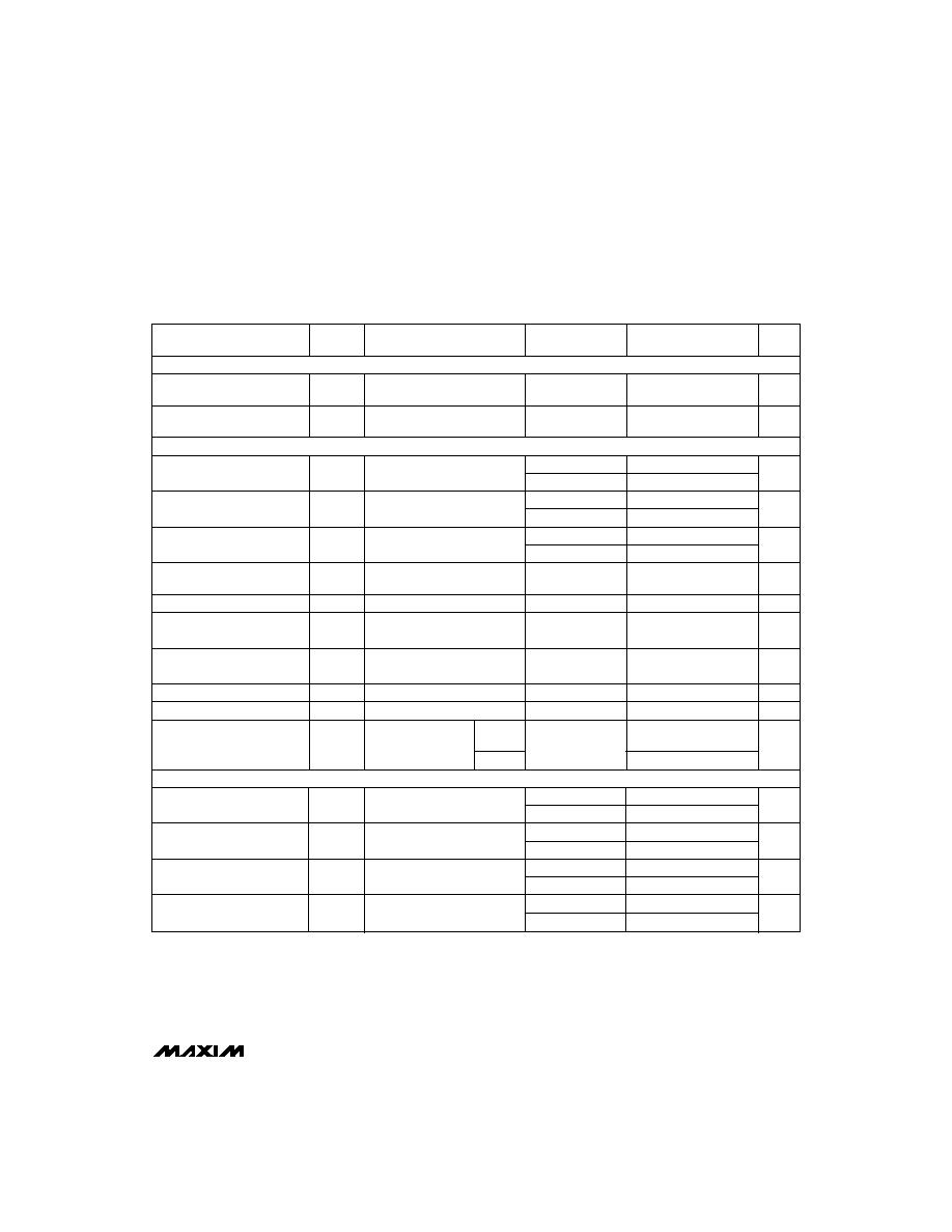
ELECTRICAL CHARACTERISTICS -- Dual Supplies
(V+ = 15V, V- = -15V, V
L
= 5V, GND = 0V, V
INL
= 0.8V, V
INH
= 2.4V, T
A
= T
MIN
to T
MAX
, unless otherwise noted.)
PARAMETER
SYMBOL
CONDITIONS
TEMP.
MIN
TYP
MAX
UNITS
(Note 2)
Analog-Signal Range
V
COM,
(Note 3)
-15
15
V
V
NO,
V
NC
V
COM
= ±12.5V,
20
35
On Resistance
R
ON
I
(NC or NO)
= -10mA,
T
A
= +25∞C
30
V+ = 13.5V, V- = -13.5V
T
A
= T
MIN
to T
MAX
45
On Resistance Match
R
ON
T
A
= +25∞C
2
Between Channels (Note 4)
T
A
= T
MIN
to T
MAX
3
On Resistance Flatness
R
ON
T
A
= +25∞C
3
(Note 4)
T
A
= T
MIN
to T
MAX
5
INC
(OFF)
V+ = 16.5V, V- = -16.5V,
T
A
= +25∞C
-0.25
0.25
NO or NC Off Leakage Current
or
V
COM
= ±15.5V,
C, E
-6
6
nA
INO
(OFF)
V
NC
or V
NO
=
±
15.5V
M
-20
20
MAX317,
T
A
= +25∞C
-0.25
-0.1
0.25
MAX318
C, E
-6
6
COM Off Leakage Current
ICOM
(OFF)
M
-20
20
nA
T
A
= +25∞C
-0.75
-0.1
0.75
MAX319
C, E
-10
10
M
-60
60
MAX317,
T
A
= +25∞C
-0.4
0.4
MAX318
C, E
-10
10
COM On Leakage Current
ICOM
(ON)
M
-40
40
nA
T
A
= +25∞C
-0.75
0.75
MAX319
C, E
-10
10
M
-60
60
ABSOLUTE MAXIMUM RATINGS
Voltage Referenced to V-
V+....................................................................................+44V
GND ................................................................................+25V
V
L
.................................................(GND - 0.3V) to (V+ + 0.3V)
IN, COM, NC, NO....................(V- - 2V) to (V+ + 2V) or 30mA,
whichever occurs first
Continuous Current (any terminal) .....................................30mA
Peak Current, NC, NO, COM
(pulsed at 1ms, 10% duty cycle max)..........................100mA
ESD .................................................................................±2000V
Continuous Power Dissipation (T
A
= +70∞C) (Note 1)
Plastic DIP (derate 9.09mW/∞C above +70∞C)............727mW
SO (derate 5.88mW/∞C above +70∞C) ........................471mW
CERDIP (derate 8.00mW/∞C above +70∞C) ................640mW
Operating Temperature Ranges:
MAX31_C_ _.......................................................0∞C to +70∞C
MAX31_E_ _ ....................................................-40∞C to +85∞C
MAX31_MJA..................................................-55∞C to +125∞C
Storage Temperature Range ............................-55∞C to +150∞C
Lead Temperature (soldering, 10sec) ............................+300∞C
Note 1:
All leads are soldered or welded to PC board.
I
(NC OR NO)
= -10mA,
V
COM
= 10V or -10V,
V+ = 15V, V- = -15V
I
(NC OR NO)
= -10mA,
V
COM
= 5V or -5V,
V+ = 15V, V- = -15V
V+ = 16.5V,
V- = -16.5V,
V
COM
= ±15.5V,
V
NC
or V
NO
= ≠
+15.5V
V+ = 16.5V,
V- = -16.5V,
V
NC
or V
NO
= V
D
=
±15.5V
M
C, E
MAX317/MAX318/MAX319
Precision, CMOS Analog Switches
_______________________________________________________________________________________
3
ELECTRICAL CHARACTERISTICS -- Dual Supplies (continued)
(V+ = 15V, V- = -15V, V
L
= 5V, GND = 0V, V
INL
= 0.8V, V
INH
= 2.4V, T
A
= T
MIN
to T
MAX
, unless otherwise noted.)
PARAMETER
SYMBOL
CONDITIONS
TEMP.
MIN
TYP
MAX
UNITS
(Note 2)
LOGIC INPUT
Logic Input Current
I
IH
V
IN
= 2.4V
-0.5
0.005
0.5
µA
(Input Voltage High)
Logic Input Current
I
IL
V
IN
= 0.8V
-0.5
0.005
0.5
µA
(Input Voltage Low)
DYNAMIC
Turn-On Time
t
ON
MAX317, MAX318, Figure 2,
T
A
= +25∞C
100
175
ns
V
COM
= ±10V
T
A
= T
MIN
to T
MAX
250
Turn-Off Time
t
OFF
MAX317, MAX318, Figure 2,
T
A
= +25∞C
60
145
ns
V
COM
= ±10V
T
A
= T
MIN
to T
MAX
210
Transition Time
t
TRANS
MAX319, Figure 3,
T
A
= +25∞C
175
ns
V
NO
= ±10V, V
NC
=
±
10V
T
A
= T
MIN
to T
MAX
250
Break-Before-Make Interval
t
D
MAX319, Figure 4,
T
A
= +25∞C
5
13
ns
V
NO
= V
NC
= ±10V
Charge Injection
Q
V
GEN
= 0V, Figure 5
T
A
= +25∞C
3
10
pC
Off Isolation (Note 5)
OIRR
R
L
= 50
, C
L
= 5pF,
T
A
= +25∞C
68
dB
f = 1MHz, Figure 7
Crosstalk (Note 6)
R
L
= 50
, C
L
= 5pF,
T
A
= +25∞C
85
dB
f = 1MHz, Figure 8
COM Off Capacitance
C
COM(OFF)
V
COM
= 0V, f = 1MHz, Figure 8
T
A
= +25∞C
8
pF
Off Capacitance NC or NO
C
(OFF)
V
COM
= 0V, f = 1MHz, Figure 8
T
A
= +25∞C
8
pF
Channel-On Capacitance
V
S
= 0V, f = 1MHz,
MAX317,
T
A
= +25∞C
30
pF
C
COM(ON)
Figure 9
MAX318
COM Terminal
MAX319
35
SUPPLY
Positive Supply Current
I+
V
IN
= 0V or 5V, V+ = 16.5V,
T
A
= +25∞C
-1
0.0001
1
µA
V- = -16.5V
T
A
= T
MIN
to T
MAX
-5
5
Negative Supply Current
I-
V
IN
= 0V or 5V, V+ = 16.5V,
T
A
= +25∞C
-1
-0.0001
1
µA
V- = -16.5V
T
A
= T
MIN
to T
MAX
-5
5
Logic Supply Current
I
L
V
IN
= 0V or 5V, V+ = 16.5V,
T
A
= +25∞C
-1
0.0001
1
µA
V- = -16.5V
T
A
= T
MIN
to T
MAX
-5
5
Ground Current
I
GND
V
IN
= 0V or 5V, V+ = 16.5V,
T
A
= +25∞C
-1
-0.0001
1
µA
V- = -16.5V
T
A
= T
MIN
to T
MAX
-5
5

MAX317/MAX318/MAX319
Precision, CMOS Analog Switches
4
_______________________________________________________________________________________
ELECTRICAL CHARACTERISTICS -- Single Supply
(V+ = 12V, V- = 0V, V
L
= 5V, GND = 0V, V
INH
= 2.4V, V
INL
= 0.8V, T
A
= +25∞C, unless otherwise noted.)
PARAMETER
SYMBOL
CONDITIONS
MIN
TYP
MAX
UNITS
(Note 2)
SWITCH
Analog-Signal Range
V
COM,
(Note 3)
0
12
V
V
NO,
V
NC
Drain-Source On Resistance
R
(ON)
I
(NC or NO)
= -10mA, V
COM
= 3.8V, V+ = 10.8V
40
100
DYNAMIC
Turn-On Time
t
ON
V
COM
= 8V, Figure 2
110
ns
Turn-Off Time
t
OFF
V
COM
= 8V, Figure 2
40
ns
Break-Before-Make
t
D
MAX319, R
L
= 1000
, C
L
= 35pF,
60
ns
Time Delay
Figure 4
Charge Injection
Q
C
L
= 10nF, V
GEN
= 0V, R
GEN
= 0V,
2
10
pC
Figure 5
SUPPLY
Positive Supply Current
I+
V+ = 13.2V, all channels on or off,
0.0001
µA
V
IN
= 0V or 5V, V
L
= 5.25V
Negative Supply Current
I-
V+ = 13.2V, all channels on or off,
0.0001
µA
V
IN
= 0V or 5V, V
L
= 5.25V
Logic Supply Current
I
L
V
L
= 5.25V, all channels on or off,
0.0001
µA
V
IN
= 0V or 5V
Ground Current
I
GND
V
L
= 5.25V, all channels on or off,
-0.0001
µA
V
IN
= 0V or 5V
Note 2:
Typical values are for
design aid only
, not guaranteed, not subject to production testing.
Note 3:
Guaranteed by design.
Note 4:
On resistance match between channels and flatness are guaranteed only with bipolar-supply operation.
Note 5:
Off Isolation = 20log
10
(
V
COM
)
, V
COM
= output, V
NC
or V
NO
= input to off switch.
V
NC
or V
NO
Note 6:
Between any two switches.

MAX317/MAX318/MAX319
Precision, CMOS Analog Switches
_______________________________________________________________________________________
5
45
5
-20
-10
10
ON RESISTANCE vs. V
COM
AND
POWER-SUPPLY VOLTAGE
15
35
MAX317-01
V
COM
(V)
R
ON
(
)
0
20
25
40
10
30
20
50
A
B
C
D
A: V+ = 5V,
V- = -5V
B: V+ = 10V,
V- = -10V
C: V+ = 15V,
V- = -15V
D: V+ = 20V,
V- = -20V
5
-20
-10
10
ON RESISTANCE vs. V
COM
AND
TEMPERATURE
30
MAX317-02
V
COM
(V)
R
ON
(
)
0
20
20
10
25
15
35
V+ = 15V
V- = -15V
T
A
= +125∞C
T
A
= +85∞C
T
A
= +25∞C
T
A
= -55∞C
20
0
5
15
ON RESISTANCE vs. V
COM
AND
TEMPERATURE
120
MAX317-03
V
COM
(V)
R
ON
(
)
10
20
80
40
100
60
140
V- = 0V
V+ = 5V
V+ = 10V
V+ = 15V
V+ = 20V
10
0
5
15
ON RESISTANCE vs. V
COM
(SINGLE-SUPPLY)
60
MAX317-04
V
COM
(V)
R
ON
(
)
10
20
40
20
50
30
70
V+ = 12V
V- = 0V
T
A
= +125∞C
T
A
= +85∞C
T
A
= +25∞C
-60
-20
CHARGE INJECTION vs.
ANALOG VOLTAGE
40
MAX317-07
V
COM
(V)
Q (pC)
0
20
0
-40
20
-20
60
-15 -10
-5
5
10
15
V+ = 15V
V- = -15V
0.0001
-55
OFF LEAKAGE CURRENTS vs.
TEMPERATURE
10
MAX317-05
TEMPERATURE (∞C)
OFF LEAKAGE
+25
+125
0.1
0.001
1
0.01
100
V+ = 16.5V
V- = -16.5V
V
COM
= ±15V
V
NC
OR V
NO
=
+15V
0.0001
-55
ON LEAKAGE CURRENTS vs.
TEMPERATURE
10
MAX317-06
TEMPERATURE (∞C)
ON LEAKAGE
+25
+125
0.1
0.001
1
0.01
100
V+ = 16.5V
V- = -16.5V
V
COM
= ±15V
V
NC
OR V
NO
= ±15V
0.0001
-55
SUPPLY CURRENT vs. TEMPERATURE
10
MAX317-08
TEMPERATURE (∞C)
I+, I-, I
L
(
µ
A)
+25
+125
0.1
0.001
1
0.01
100
A: I+ at V+ = 16.5V
B: I- at V- = -16.5V
C: I
L
at V
L
= 5V
A
B
C
__________________________________________Typical Operating Characteristics
(T
A
= +25∞C, unless otherwise noted).