 | –≠–ª–µ–∫—Ç—Ä–æ–Ω–Ω—ã–π –∫–æ–º–ø–æ–Ω–µ–Ω—Ç: MAX321 | –°–∫–∞—á–∞—Ç—å:  PDF PDF  ZIP ZIP |

_______________General Description
The MAX320/MAX321/MAX322 are precision, dual,
SPST analog switches designed to operate from ±3V to
±8V dual supplies. The MAX320 has two normally open
(NO) switches and the MAX321 has two normally
closed (NC) switches. The MAX322 has one NO and
one NC switch. Low power consumption (1.25mW)
makes these parts ideal for battery-powered equip-
ment. They offer low leakage currents (100pA max) and
fast switching speeds (t
ON
= 150ns max, t
OFF
= 100ns
max).
The MAX320 series, powered from ±5V supplies, offers
35
max on-resistance (R
ON
), 2
max matching
between channels, and 4
max R
ON
flatness.
These switches also offer 5pC max charge injection
and a minimum of 2000V ESD protection per Method
3015.7.
For equivalent devices specified for single-supply oper-
ation, see the MAX323/MAX324/MAX325 data sheet.
For quad versions of these switches, see the
MAX391/MAX392/MAX393 data sheet.
________________________Applications
Battery-Operated Systems
Sample-and-Hold Circuits
Heads-Up Displays
Guidance and Control Systems
Audio and Video Switching
Military Radios
Test Equipment
Communications Systems
±5V DACs and ADCs
PBX, PABX
____________________________Features
o
Low On-Resistance, 35
max (16
typical)
o
R
ON
Matching Between Channels <2
o
R
ON
Flatness <4
o
Guaranteed Charge Injection <5pC
o
Bipolar Supply Operation (±3V to ±8V)
o
Low Power Consumption, <1.25mW
o
Low Leakage Current Over Temperature,
<2.5nA at +85∞C
o
Fast Switching, t
ON
<150ns, t
OFF
<100ns
o
Guaranteed Break-Before-Make (MAX322 only)
______________Ordering Information
MAX320/MAX321/MAX322
Precision, Dual-Supply, SPST
Analog Switches
________________________________________________________________
Maxim Integrated Products
1
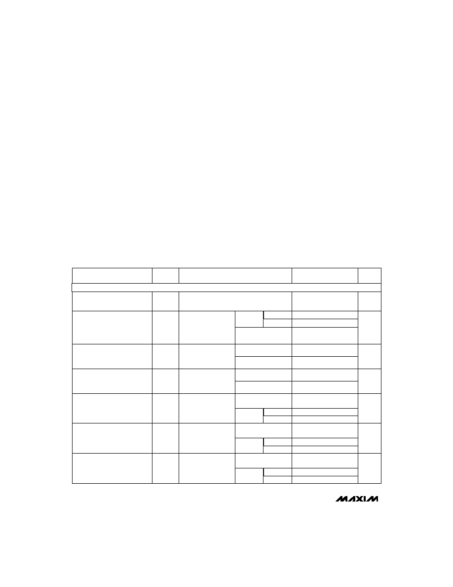
SWITCHES SHOWN FOR LOGIC "0" INPUT
MAX321
LOGIC
SWITCH
0
1
ON
OFF
TOP VIEW
DIP/SO/
µ
MAX
MAX320
LOGIC
SWITCH
0
1
OFF
ON
MAX322
LOGIC
SWITCH 1
0
1
OFF
ON
SWITCH 2
ON
OFF
8
7
6
5
1
2
3
4
V+
IN1
COM2
NO2
V-
IN2
COM1
NO1
MAX320
DIP/SO/
µ
MAX
8
7
6
5
1
2
3
4
V+
IN1
COM2
NC2
V-
IN2
COM1
NC1
MAX321
DIP/SO/
µ
MAX
8
7
6
5
1
2
3
4
V+
IN1
COM2
NC2
V-
IN2
COM1
NO1
MAX322
_____________________Pin Configurations/Functional Diagrams/Truth Tables
Call toll free 1-800-998-8800 for free samples or literature.
19-0350; Rev 0; 12/94
Ordering Information continued at end of data sheet.
* Contact factory for dice specifications.
** Contact factory for availability.
8 CERDIP**
-55∞C to +125∞C
MAX320MJA
8 CERDIP**
-40∞C to +85∞C
MAX320EJA
8 SO
-40∞C to +85∞C
MAX320ESA
8 Plastic DIP
-40∞C to +85∞C
MAX320EPA
Dice*
0∞C to +70∞C
MAX320C/D
8 SO
0∞C to +70∞C
MAX320CSA
8 Plastic DIP
0∞C to +70∞C
MAX320
CPA
PIN-PACKAGE
TEMP. RANGE
PART
8 µMAX
0∞C to +70∞C
MAX320CUA
Voltage Referenced to V-
V+ ................................................................(V- - 0.3V) to +17V
IN_, COM_, NC_, NO_ (Note 1) .........(V- - 0.3V) to (V+ + 0.3V)
Continuous Current (any terminal) ......................................30mA
Peak Current, COM_, NO_, NC_
(pulsed at 1ms, 10% duty cycle max) ..............................100mA
ESD per Method 3015.7 ..................................................>2000V
Continuous Power Dissipation
Plastic DIP (derate 9.09mW/∞C above +70∞C) .............727mW
Narrow SO (derate 5.88mW/∞C above +70∞C) .............471mW
µMAX (derate 4.10mW/∞C above +70∞C) .....................330mW
CERDIP (derate 8.00mW/∞C above +70∞C) ..................640mW
Operating Temperature Ranges
MAX32_C_ _ ........................................................0∞C to +70∞C
MAX32_E_ _......................................................-40∞C to +85∞C
MAX32_MJA ...................................................-55∞C to +125∞C
Storage Temperature Range .............................-65∞C to +150∞C
Lead Temperature (soldering, 10sec) .............................+300∞C
MAX320/MAX321/MAX322
Precision, Dual-Supply, SPST
Analog Switches
2
_______________________________________________________________________________________
Stresses beyond those listed under "Absolute Maximum Ratings" may cause permanent damage to the device. These are stress ratings only, and functional
operation of the device at these or any other conditions beyond those indicated in the operational sections of the specifications is not implied. Exposure to
absolute maximum rating conditions for extended periods may affect device reliability.
ABSOLUTE MAXIMUM RATINGS
Note 1:
Signals on NC_, NO_, COM_, or IN_ exceeding V+ or V- are clamped by internal diodes. Limit forward diode current to
maximum current rating.
ELECTRICAL CHARACTERISTICS
(V+ = +5V ±10%, V- = -5V ±10%, V
INH
= 3.5V, V
INL
= 2.5V, T
A
= T
MIN
to T
MAX
, unless otherwise noted.)
-10
10
-50
50
COM On Leakage Current
(Note 6)
nA
PARAMETER
SYMBOL
MIN
TYP
MAX
(Note 2)
UNITS
On-Resistance
R
ON
45
16
35
0.3
2
On-Resistance Match Between
Channels (Note 4)
R
ON
Analog Signal Range
V
COM
,
V
NO
,
V
NC
V-
V+
V
On-Resistance Flatness
(Note 5)
R
FLAT(ON)
1
4
-0.1
0.01
0.1
NO or NC Off Leakage Current
(Note 6)
I
NO(OFF)
or
I
NC(OFF)
nA
-5
5
COM Off Leakage Current
(Note 6)
-5
5
nA
I
COM(OFF)
I
COM(ON)
CONDITIONS
V+ = 5V, V- = -5V,
I
COM
= 1.0mA,
V
NO
or V
NC
= ±3V
V+ = 4.5V,
V- = -4.5V,
I
COM
= 1.0mA,
V
NO
or V
NC
= ±3.5V
V+ = 5V, V- = -5V,
I
COM
= 1.0mA,
V
NO
or V
NC
= ±3V
V+ = 5.5V,
V- = -5.5V,
V
COM
= ±4.5V,
V
NO
or V
NC
= 4.5V
(Note 3)
V+ = 5.5V,
V- = -5.5V,
V
COM
= ±4.5V,
V
NO
or V
NC
= 4.5V
V+ = 5.5V,
V- = -5.5V,
V
COM
= ±4.5V,
V
NO
or V
NC
= ±4.5V
T
A
= +25∞C
T
A
= +25∞C
T
A
= +25∞C
T
A
= T
MIN
to T
MAX
T
A
= +25∞C
T
A
= T
MIN
to T
MAX
T
A
= +25∞C
T
A
= T
MIN
to T
MAX
T
A
=
+25∞C
T
A
= T
MIN
to T
MAX
C, E
C, E
C, E
T
A
= T
MIN
to T
MAX
T
A
= T
MIN
to T
MAX
M
M
M
4
6
-0.1
0.01
0.1
-40
40
-40
40
-0.2
0.05
0.2
C, E
M
16
30
ANALOG SWITCH
±
±

MAX320/MAX321/MAX322
Precision, Dual-Supply, SPST
Analog Switches
_______________________________________________________________________________________
3
ELECTRICAL CHARACTERISTICS
(V+ = +5V ±10%, V- = -5V ±10%, V
INH
= 3.5V, V
INL
= 2.5V, T
A
= T
MIN
to T
MAX
, unless otherwise noted.)
PARAMETER
SYMBOL
MIN
TYP
MAX
(Note 2)
UNITS
Input Current with Input
Voltage High
I
INH
-0.5
0.005
0.5
µA
CONDITIONS
Input Current with Input
Voltage Low
I
INL
-0.5
0.005
0.5
µA
Turn-On Time
t
ON
65
150
ns
Charge Injection
(Note 3)
Q
2
5
pC
C
L
= 1.0nF, V
GEN
= 0V,
R
GEN
= 0
, Figure 4
T
A
= +25∞C
T
A
= T
MIN
to T
MAX
175
V
COM
= ±3V, Figure 2
T
A
= +25∞C
T
A
= T
MIN
to T
MAX
150
V
COM
= ±3V, Figure 2
Turn-Off Time
t
OFF
35
100
ns
Power-Supply Range
MAX322 only, R
L
= 300
, C
L
= 35pF, Figure 3
Break-Before-Make
Time Delay (Note 3)
t
D
2
5
ns
T
A
= +25∞C
T
A
= +25∞C
R
L
= 50
, C
L
= 5pF,
f = 1MHz, Figure 5
Off Isolation (Note 7)
OIRR
72
dB
T
A
= +25∞C
R
L
= 50
, C
L
= 5pF,
f = 1MHz, Figure 6
Crosstalk (Note 8)
85
dB
T
A
= +25∞C
f = 1MHz, Figure 7
NC or NO Capacitance
C
(OFF)
9
pF
T
A
= +25∞C
f = 1MHz, Figure 7
COM Off Capacitance
C
COM(OFF)
9
pF
T
A
= +25∞C
f = 1MHz, Figure 8
COM On Capacitance
C
COM(ON)
pF
±2.7
±8
V
Positive Supply Current
22
I+
V+ = 5.5V, V- = -5.5V,
V
IN
= 0V or V+,
all channels on or off
T
A
= T
MIN
to T
MAX
-200
200
µA
Negative Supply
Current
I-
V+ = 5.5V, V- = -5.5V,
V
IN
= 0V or V+,
all channels on or off
T
A
= +25∞C
-125
80
125
µA
Note 2:
The algebraic convention where the most negative value is a minimum and the most positive value a maximum is used in
this data sheet.
Note 3:
Guaranteed by design.
Note 4:
R
ON
=
R
ON
max -
R
ON
min.
Note 5:
Flatness is defined as the difference between the maximum and minimum value of on-resistance as measured over the
specified analog signal range.
Note 6:
Leakage parameters are 100% tested at maximum rated hot temperature and guaranteed by correlation at +25∞C.
Note 7:
Off Isolation = 20 log
10
[ V
COM
/ (V
NC or
V
NO
) ], V
COM
= output, V
NC or
V
NO
= input to off switch.
Note 8:
Between any two switches.
T
A
= T
MIN
to T
MAX
T
A
= +25∞C
-200
200
-125
80
125
Input Voltage High
V
INH
3.5
V
3V < V+ < 8V, V-
0V
V+ = 5V ±10%, V-
0V
V+ - 1.5
Input Voltage Low
V
INL
2.5
V
3V < V+ < 8V, V-
0V
V+ = 5V ±10%, V-
0V
V+ - 2.5
LOGIC INPUT
DYNAMIC
SUPPLY
MAX320/MAX321/MAX322
Precision, Dual-Supply, SPST
Analog Switches
4
_______________________________________________________________________________________
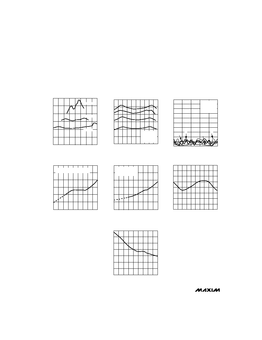
__________________________________________Typical Operating Characteristics
(V+ = +5V, V- = -5V, T
A
= +25∞C, unless otherwise noted.)
0.0001
-55
65
85
OFF LEAKAGE CURRENT vs. TEMPERATURE
10
MAX320-05
TEMPERATURE (∞C)
OFF LEAKAGE CURRENT (nA)
-15
5
25
45
-35
105 125
0.1
0.001
1
0.01
100
V+ = +5.5V, V- = -5.5V
V
COM
= ±4.5V
V
NC
or V
NO
= 4.5V
±
0
-8
-6
0
2
ON-RESISTANCE vs. VOLTAGE AT COM PIN
30
MAX320-01
V
COM
(V)
R
ON
(
)
-4
-2
4
6
8
20
5
25
10
15
V± = ±3V
V± = ±5V
V± = ±8V
0
-5
-3
-4
-2
3
4
ON-RESISTANCE vs. VOLTAGE AT COM PIN
(OVER TEMPERATURE)
30
MAX320-02
V
COM
(V)
R
ON
(
)
-1
0
1
2
5
20
5
25
15
10
A: T
A
= +125∞C
B: T
A
= +85∞C
C: T
A
= +25∞C
D: T
A
= -55∞C
D
C
B
A
0
-5
-1
ON-RESISTANCE MATCH vs. VOLTAGE
AT COM PIN (OVER TEMPERATURE)
MAX320-03
V
COM
(V)
R
ON
(
)
1
3
0.30
0.35
0.10
0.05
0.40
0.45
0.20
0.25
0.15
0.50
5
-3
A: T
A
= -55∞C
B: T
A
= +25∞C
C: T
A
= +85∞C
D: T
A
= +125∞C
C
A
B
D
0.0001
-55
65
85
ON LEAKAGE CURRENT vs. TEMPERATURE
10
MAX320-04
TEMPERATURE (∞C)
ON LEAKAGE CURRENT (nA)
-15
5
25
45
-35
105 125
0.1
0.001
1
0.01
100
V+ = +5.5V, V- = -5.5V
V
COM
= ±4.5V, V
NC
or V
NO
= ±4.5V
0
-55
65
85
SUPPLY CURRENT vs. TEMPERATURE
100
120
MAX320-07
TEMPERATURE (∞C)
I
SUPPLY
(
µ
A)
25
45
-35 -15
5
105 125
80
20
40
60
140
-20
-5
CHARGE INJECTION vs.
VOLTAGE AT COM PIN
15
MAX320-06
V
COM
(V)
Q (pC)
-1
0
5
0
-15
10
5
-10
-5
20
-4
-3
-2
1
2
3
4
MAX320/MAX321/MAX322
Precision, Dual-Supply, SPST
Analog Switches
_______________________________________________________________________________________
5
__________Applications Information
Logic Levels
Calculate the logic thresholds typically as follows: V
IH
=
(V+ - 1.5V) and V
IL
= (V+ - 2.5V).
Power-supply consumption is minimized when IN1 and
IN2 are driven with logic-high levels equal to V+ and logic-
low levels well below the calculated V
IL
of (V+ - 2.5V). IN1
and IN2 can be driven to V- without damage.
Analog Signal Levels
Analog signals that range over the entire supply voltage
(V- to V+) can be switched, with very little change in on-
resistance over the entire voltage range (see
Typical
Operating Characteristics). All switches are bidirec-
tional, so NO_, NC_, and COM_ pins can be used as
either inputs or outputs.
Power-Supply Sequencing
and Overvoltage Protection
Do not exceed the absolute maximum ratings, because
stresses beyond the listed ratings may cause perma-
nent damage to the devices.
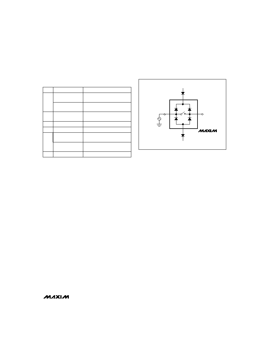
Proper power-supply sequencing is recommended for
all CMOS devices. Always apply V+, followed by V-,
before applying analog signals or logic inputs, especial-
ly if the analog or logic signals are not current-limited. If
this sequencing is not possible, and if the analog or
logic inputs are not current-limited to <30mA, add two
small signal diodes (D1, D2) as shown in Figure 1.
Adding protection diodes reduces the analog signal
range to a diode drop (about 0.7V) below V+ for D1,
and a diode drop above V- for D2. Leakage is not
affected by adding the diodes. On-resistance increas-
es by a small amount at low supply voltages. Maximum
supply voltage (V- to V+) must not exceed 17V.
Adding protection diode D1 causes the logic thresh-
olds to be shifted relative to the positive power-supply
rail. This can be significant when low positive supply
voltages (+5V or less) are used. Driving IN1 and IN2 all
the way to the supply rails (i.e., to a diode drop higher
than the V+ pin or a diode drop lower than the V- pin) is
always acceptable.
The protection diodes D1 and D2 also protect against
some overvoltage situations. With the circuit of Figure 1,
if the supply voltage is below the absolute maximum
rating and if a fault voltage up to the absolute maximum
rating is applied to an analog signal pin, no damage
will result. For example, with ±5V supplies, analog sig-
nals up to ±8.5V will not damage the circuit of Figure 1.
If only a single fault signal is present, the fault voltage
can rise to +12V or to -12V without damage.
_____________________Pin Description
POSITIVE SUPPLY
COM
D1
D2
NO
V-
Vg
V+
NEGATIVE SUPPLY
MAX320
MAX321
MAX322
Figure 1. Overvoltage Protection Using Two External Blocking
Diodes
5
Normally Closed Analog
Switch Terminal
NC2
(MAX321/MAX322)
Normally Open Analog
Switch Terminal
NO2
(MAX320)
Negative Supply
V-
4
Logic Inputs
IN2, IN1
3, 7
PIN
Analog Switch Common
Terminals
COM1, COM2
2, 6
Normally Closed Analog
Switch Terminal
NC1
(MAX321)
Normally Open Analog
Switch Terminal
NO1
(MAX320/MAX322)
1
FUNCTION
NAME
Positive Supply
V+
8