General Description
The MAX3222E/MAX3232E/MAX3237E/MAX3241E/
MAX3246E +3.0V-powered EIA/TIA-232 and V.28/V.24
communications interface devices feature low power con-
sumption, high data-rate capabilities, and enhanced
electrostatic-discharge (ESD) protection. The enhanced
ESD structure protects all transmitter outputs and
receiver inputs to ±15kV using IEC 1000-4-2 Air-Gap
Discharge, ±8kV using IEC 1000-4-2 Contact Discharge
(±9kV for MAX3246E), and ±15kV using the Human Body
Model. The logic and receiver I/O pins of the MAX3237E
are protected to the above standards, while the transmit-
ter output pins are protected to ±15kV using the Human
Body Model.
A proprietary low-dropout transmitter output stage delivers
true RS-232 performance from a +3.0V to +5.5V power
supply, using an internal dual charge pump. The charge
pump requires only four small 0.1µF capacitors for opera-
tion from a +3.3V supply. Each device guarantees opera-
tion at data rates of 250kbps while maintaining RS-232
output levels. The MAX3237E guarantees operation at
250kbps in the normal operating mode and 1Mbps in the
MegaBaudTM operating mode, while maintaining RS-232-
compliant output levels.
The MAX3222E/MAX3232E have two receivers and two
transmitters. The MAX3222E features a 1µA shutdown
mode that reduces power consumption in battery-pow-
ered portable systems. The MAX3222E receivers remain
active in shutdown mode, allowing monitoring of external
devices while consuming only 1µA of supply current. The
MAX3222E and MAX3232E are pin, package, and func-
tionally compatible with the industry-standard MAX242
and MAX232, respectively.
The MAX3241E/MAX3246E are complete serial ports
(three drivers/five receivers) designed for notebook and
subnotebook computers. The MAX3237E (five drivers/
three receivers) is ideal for peripheral applications that
require fast data transfer. These devices feature a shut-
down mode in which all receivers remain active, while
consuming only 1µA (MAX3241E/MAX3246E) or 10nA
(MAX3237E).
The MAX3222E, MAX3232E, and MAX3241E are avail-
able in space-saving SO, SSOP, and TSSOP packages.
The MAX3237E is offered in an SSOP package. The
MAX3246E is offered in the ultra-small 6 x 6 UCSPTM
package.
________________________Applications
Battery-Powered Equipment
Printers
Cell Phones
Smart Phones
Cell-Phone Data Cables
xDSL Modems
Notebook, Subnotebook,
and Palmtop Computers
Features
o ESD Protection for RS-232 I/O Pins
(MAX3222E/MAX3232E/MAX3241E/MAX3246E)
±15kV--Human Body Model
±8kV--IEC 1000-4-2, Contact Discharge
±9kV (MAX3246E Only)--IEC 1000-4-2, Contact
Discharge
±15kV--IEC 1000-4-2, Air-Gap Discharge
o ESD Protection for all Logic and Receiver I/O Pins
(MAX3237E)
±15kV--Human Body Model
±8kV--IEC 1000-4-2, Contact Discharge
±15kV≠IEC 1000-4-2, Air-Gap Discharge
o ESD Protection for Transmitter Output Pins
(MAX3237E)
±15kV--Human Body Model
o Guaranteed Data Rate
250kbps (MAX3222E/MAX3232E/MAX3241E/
MAX3246E/MAX3237E, Normal Operation)
1Mbps (MAX3237E, MegaBaud Operation)
o Latchup Free
o Low-Power Shutdown with Receivers Active
1µA (MAX3222E/MAX3241E/MAX3246E)
10nA (MAX3237E)
o Flow-Through Pinout (MAX3237E)
o Guaranteed Mouse Drivability (MAX3241E)
o Meets EIA/TIA-232 Specifications Down to +3.0V
MAX3222E/MAX3232E/MAX3237E/MAX3241E
/MAX3246E
±15kV ESD-Protected, Down to 10nA, 3.0V to 5.5V,
Up to 1Mbps, True RS-232 Transceivers
________________________________________________________________ Maxim Integrated Products
1
19-1298; Rev 7; 2/03
_______________Ordering Information
Ordering Information continued at end of data sheet.
Pin Configurations appear at end of data sheet.
Selector Guide appears at end of data sheet.
Typical Operating Circuits appear at end of data sheet.
For pricing, delivery, and ordering information, please contact Maxim/Dallas Direct! at
1-888-629-4642, or visit Maxim's website at www.maxim-ic.com.
PART
TEMP RANGE
PIN-PACKAGE
MAX3222ECUP
0∞C to +70∞C
20 TSSOP
MAX3222ECAP
0∞C to +70∞C
20 SSOP
MegaBaud is a trademark of Maxim Integrated Products, Inc.
UCSP is a trademark of Maxim Integrated Products, Inc.
Covered by U.S. Patent numbers 4,636,930; 4,679,134;
4,777,577; 4,797,899; 4,809,152; 4,897,774; 4,999,761; and
other patents pending.
MAX3222E/MAX3232E/MAX3237E/MAX3241E
/MAX3246E
±15kV ESD-Protected, Down to 10nA, 3.0V to 5.5V,
Up to 1Mbps, True RS-232 Transceivers
2
_______________________________________________________________________________________
ABSOLUTE MAXIMUM RATINGS
ELECTRICAL CHARACTERISTICS
(V
CC
= +3V to +5.5V, C1≠C4 = 0.1µF, T
A
= T
MIN
to T
MAX
, unless otherwise noted. Typical values are at T
A
= +25∞C.) (Notes 3, 4)
Stresses beyond those listed under "Absolute Maximum Ratings" may cause permanent damage to the device. These are stress ratings only, and functional
operation of the device at these or any other conditions beyond those indicated in the operational sections of the specifications is not implied. Exposure to
absolute maximum rating conditions for extended periods may affect device reliability.
V
CC
to GND ..............................................................-0.3V to +6V
V+ to GND (Note 1) ..................................................-0.3V to +7V
V- to GND (Note 1) ...................................................+0.3V to -7V
V+ + |V-| (Note 1).................................................................+13V
Input Voltages
T_IN, EN, SHDN, MBAUD to GND ........................-0.3V to +6V
R_IN to GND .....................................................................±25V
Output Voltages
T_OUT to GND...............................................................±13.2V
R_OUT, R_OUTB (MAX3241E)................-0.3V to (V
CC
+ 0.3V)
Short-Circuit Duration, T_OUT to GND.......................Continuous
Continuous Power Dissipation (T
A
= +70∞C)
16-Pin SSOP (derate 7.14mW/∞C above +70∞C) ..........571mW
16-Pin Wide SO (derate 9.52mW/∞C above +70∞C) .....762mW
18-Pin Wide SO (derate 9.52mW/∞C above +70∞C) .....762mW
18-Pin PDIP (derate 11.11mW/∞C above +70∞C)..........889mW
20-Pin TSSOP (derate 10.9mW/∞C above +70∞C) ........879mW
20-Pin SSOP (derate 8.00mW/∞C above +70∞C) ..........640mW
28-Pin SSOP (derate 9.52mW/∞C above +70∞C) ..........762mW
28-Pin Wide SO (derate 12.50mW/∞C above +70∞C) .............1W
28-Pin TSSOP (derate 12.8mW/∞C above +70∞C) ......1026mW
32-Lead QFN (derate 23.2mW/∞C above +70∞C) .........1860mW
6 x 6 UCSP (derate 12.6mW/∞C above +70∞C) .............1010mW
Operating Temperature Ranges
MAX32_ _EC_ _ ...................................................0∞C to +70∞C
MAX32_ _EE_ _.................................................-40∞C to +85∞C
Storage Temperature Range .............................-65∞C to +150∞C
Lead Temperature (soldering, 10s) .................................+300∞C
Bump Reflow Temperature (Note 2)
Infrared, 15s..................................................................+200∞C
Vapor Phase, 20s..........................................................+215∞C
Note 1: V+ and V- can have maximum magnitudes of 7V, but their absolute difference cannot exceed 13V.
Note 2: This device is constructed using a unique set of packaging techniques that impose a limit on the thermal profile the device
can be exposed to during board-level solder attach and rework. This limit permits only the use of the solder profiles recom-
mended in the industry-standard specification, JEDEC 020A, paragraph 7.6, Table 3 for IR/VPR and convection reflow.
Preheating is required. Hand or wave soldering is not allowed.
PARAMETER
CONDITIONS
MIN
TYP
MAX
UNITS
DC CHARACTERISTICS (V
CC
= +3.3V or +5V, T
A
= +25∞C)
MAX3222E, MAX3232E,
MAX3241E, MAX3246E
0.3
1
Supply Current
SHDN = V
CC
, no load
MAX3237E
0.5
2.0
mA
SHDN = GND
1
10
µA
Shutdown Supply Current
SHDN = R_IN = GND, T_IN = GND or V
CC
(MAX3237E)
10
300
nA
LOGIC INPUTS
Input Logic Low
T_IN, EN, SHDN, MBAUD
0.8
V
V
CC
= +3.3V
2.0
Input Logic High
T_IN, EN, SHDN, MBAUD
V
CC
= +5.0V
2.4
V
Transmitter Input Hysteresis
0.5
V
T_IN, EN, SHDN
MAX3222E, MAX3232E,
MAX3241E, MAX3246E
±0.01
±1
Input Leakage Current
T_IN, SHDN, MBAUD
MAX3237E (Note 5)
9
18
µA
RECEIVER OUTPUTS
Output Leakage Current
R_OUT (MAX3222E/MAX3237E/MAX3241E/
MAX3246E), EN = V
CC
, receivers disabled
±0.05
±10
µA
Output Voltage Low
IOUT = 1.6mA (MAX3222E/MAX3232E/MAX3241E/
MAX3246E), IOUT = 1.0mA (MAX3237E)
0.4
V

MAX3222E/MAX3232E/MAX3237E/MAX3241E
/MAX3246E
±15kV ESD-Protected, Down to 10nA, 3.0V to 5.5V,
Up to 1Mbps, True RS-232 Transceivers
_______________________________________________________________________________________
3
ELECTRICAL CHARACTERISTICS (continued)
(V
CC
= +3V to +5.5V, C1≠C4 = 0.1µF, T
A
= T
MIN
to T
MAX
, unless otherwise noted. Typical values are at T
A
= +25∞C.) (Notes 3, 4)
PARAMETER
CONDITIONS
MIN
TYP
MAX
UNITS
Output Voltage High
IOUT = -1.0mA
V
CC
-
0.6
V
CC
-
0.1
V
RECEIVER INPUTS
Input Voltage Range
-25
+25
V
V
CC
= +3.3V
0.6
1.1
Input Threshold Low
T
A
= +25∞C
V
CC
= +5.0V
0.8
1.5
V
V
CC
= +3.3V
1.5
2.4
Input Threshold High
T
A
= +25∞C
V
CC
= +5.0V
2.0
2.4
V
Input Hysteresis
0.5
V
Input Resistance
T
A
= +25∞C
3
5
7
k
TRANSMITTER OUTPUTS
Output Voltage Swing
All transmitter outputs loaded with 3k
to ground
±5
±5.4
V
Output Resistance
V
CC
= 0, transmitter output = ±2V
300
50k
Output Short-Circuit Current
±60
mA
Output Leakage Current
V
C C
= 0 or + 3.0V to + 5.5V , V
OU T
= ± 12V , tr ansm i tter s
d i sab l ed ( M AX 3222E /M AX 3232E /M AX 3241E /M AX 3246E )
±25
µA
MOUSE DRIVABILITY (MAX3241E)
Transmitter Output Voltage
T1IN = T2IN = GND, T3IN = V
CC
, T3OUT loaded with
3k
to GND, T1OUT and T2OUT loaded with 2.5mA
each
±5
V
ESD PROTECTION
Human Body Model
±15
IEC 1000-4-2 Air-Gap Discharge (except MAX3237E)
±15
IEC 1000-4-2 Contact Discharge (except MAX3237E)
±8
R_IN, T_OUT
IEC 1000-4-2 Contact Discharge (MAX3246E only)
±9
kV
Human Body Model
±15
IEC1000-4-2 Air-Gap Discharge
±15
T_IN, R_IN, R_OUT, EN, SHDN,
MBAUD
MAX3237E
IEC1000-4-2 Contact Discharge
±8
kV

MAX3222E/MAX3232E/MAX3237E/MAX3241E
/MAX3246E
±15kV ESD-Protected, Down to 10nA, 3.0V to 5.5V,
Up to 1Mbps, True RS-232 Transceivers
4
_______________________________________________________________________________________
TIMING CHARACTERISTICS--MAX3237E
(V
CC
= +3V to +5.5V, C1≠C4 = 0.1µF, T
A
= T
MIN
to T
MAX
, unless otherwise noted. Typical values are at T
A
= +25∞C.) (Note 3)
Note 3: MAX3222E/MAX3232E/MAX3241E: C1≠C4 = 0.1µF tested at +3.3V ±10%; C1 = 0.047µF, C2, C3, C4 = 0.33µF tested at +5.0V
±10%. MAX3237E: C1≠C4 = 0.1µF tested at +3.3V ±5%, C1≠C4 = 0.22µF tested at +3.3V ±10%; C1 = 0.047µF, C2, C3, C4 =
0.33µF tested at +5.0V ±10%. MAX3246E; C1-C4 = 0.22µF tested at +3.3V ±10%; C1 = 0.22µF, C2, C3, C4 = 0.54µF tested at
5.0V ±10%.
Note 4: MAX3246E devices are production tested at +25∞C. All limits are guaranteed by design over the operating temperature range.
Note 5: The MAX3237E logic inputs have an active positive feedback resistor. The input current goes to zero when the inputs are at
the supply rails.
Note 6: Transmitter skew is measured at the transmitter zero crosspoints.
PARAMETER
CONDITIONS
MIN
TYP
MAX
UNITS
R
L
= 3k
, C
L
= 1000pF, one transmitter switching,
MBAUD = GND
250
V
CC
= +3.0V to +4.5V, R
L
= 3k
, C
L
= 250pF,
one transmitter switching, MBAUD = V
CC
1000
Maximum Data Rate
V
CC
= +4.5V to +5.5V, R
L
= 3k
, C
L
= 1000pF,
one transmitter switching, MBAUD = V
CC
1000
kbps
t
PHL
0.15
Receiver Propagation Delay
R_IN to R_OUT, C
L
= 150pF
t
PLH
0.15
µs
Receiver Output Enable Time
Normal operation
2.6
Receiver Output Disable Time
Normal operation
2.4
µs
| t
PHL
- t
PLH
|, MBAUD = GND (Note 6)
Transmitter Skew
| t
PHL
- t
PLH
|, MBAUD = V
CC
(Note 6)
100
ns
Receiver Skew
| t
PHL
- t
PLH
|
50
ns
MBAUD = GND
6
30
C
L
= 150pF
to 1000pF
MBAUD = V
CC
24
150
V
CC
= +3.3V,
R
L
= 3k
to 7k,
+3.0V to ≠3.0V or
-3.0V to +3.0V,
T
A
= +25∞C
C
L
= 150pF to 2500pF,
MBAUD = GND
4
30
V/µs
Transition-Region Slew Rate
TIMING CHARACTERISTICS--MAX3222E/MAX3232E/MAX3241E/MAX3246E
(V
CC
= +3V to +5.5V, C1≠C4 = 0.1µF, T
A
= T
MIN
to T
MAX
, unless otherwise noted. Typical values are at T
A
= +25∞C.) (Notes 3, 4)
PARAMETER
SYMBOL
CONDITIONS
MIN
TYP
MAX
UNITS
T
A
= T
MIN
to T
MAX
(MAX3222E/MAX3232E/
MAX3241E)
250
Maximum Data Rate
R
L
= 3k
,
C
L
= 1000pF,
one transmitter
switching
T
A
= + 25∞C ( M AX 3246E ) 250
kbps
t
PHL
0.15
Receiver Propagation Delay
t
PLH
Receiver input to receiver output,
C
L
= 150pF
0.15
µs
Receiver Output Enable Time
Normal operation (except MAX3232E)
200
ns
Receiver Output Disable Time
Normal operation (except MAX3232E)
200
ns
Transmitter Skew
|t
PHL
- t
PLH
|
(Note 6)
100
ns
Receiver Skew
|t
PHL
- t
PLH
|
50
ns
Transition-Region Slew Rate
V
C C
= + 3.3V , T
A
= + 25∞C ,
R
L
= 3k
to 7k , m easur ed
fr om + 3.0V to ≠3.0V or ≠3.0V to
+ 3.0V , one tr ansm i tter sw i tchi ng
C
L
= 150pF
to 1000pF
6
30
V/µs
MAX3222E/MAX3232E/MAX3237E/MAX3241E
/MAX3246E
±15kV ESD-Protected, Down to 10nA, 3.0V to 5.5V,
Up to 1Mbps, True RS-232 Transceivers
_______________________________________________________________________________________
5
-6
-4
-2
0
2
4
6
0
MAX3237E
TRANSMITTER OUTPUT VOLTAGE
vs. LOAD CAPACITANCE (MBAUD = GND)
MAX3237E toc07
LOAD CAPACITANCE (pF)
TRANSMITTER OUTPUT VOLTAGE (V)
1000
1500
500
2000
2500
3000
FOR DATA RATES UP TO 250kbps
1 TRANSMITTER AT 250kbps
4 TRANSMITTERS AT 15.6kbps
ALL TRANSMITTERS LOADED
WITH 3k
+ C
L
5
3
1
-1
-3
-5
V
OUT+
V
OUT-
-6
-2
-4
2
0
4
6
-5
-3
1
-1
3
5
0
1000
1500
500
2000
2500
3000
MAX3246E toc07A
LOAD CAPACITANCE (pF)
TRANSMITTER OUTPUT VOLTAGE (V)
V
OUT-
V
OUT
+
FOR DATA RATES UP TO 250kbps
1 TRANSMITTER 250kbps
4 TRANSMITTERS 15.6kbps
ALL TRANSMITTERS LOADED
WITH 3k
+ C
L
MAX3237E
TRANSMITTER OUTPUT VOLTAGE
vs. LOAD CAPACITANCE
-7.5
-5.0
-2.5
0
2.5
5.0
7.5
0
MAX3237E
TRANSMITTER OUTPUT VOLTAGE
vs. LOAD CAPACITANCE (MBAUD = V
CC
)
MAX3237E toc08
LOAD CAPACITANCE (pF)
TRANSMITTER OUTPUT VOLTAGE (V)
500
1000
1500
2000
1 TRANSMITTER AT FULL DATA RATE
4 TRANSMITTERS AT 1/16 DATA RATE
3k
+ C
L
LOAD, EACH OUTPUT
2Mbps
1.5Mbps
1Mbps
2Mbps
1Mbps
1.5Mbps
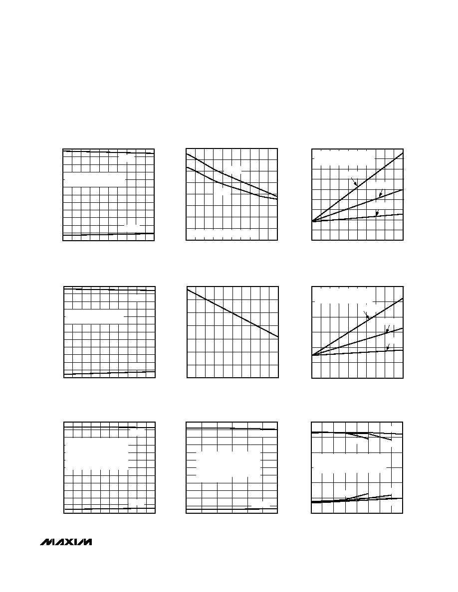
__________________________________________Typical Operating Characteristics
(V
CC
= +3.3V, 250kbps data rate, 0.1µF capacitors, all transmitters loaded with 3k
and C
L
, T
A
= +25∞C, unless otherwise noted.)
-6
-5
-4
-3
-2
-1
0
1
2
3
4
5
6
0
1000
2000
3000
4000
5000
MAX3241E
TRANSMITTER OUTPUT VOLTAGE
vs. LOAD CAPACITANCE
MAX3237E to04
LOAD CAPACITANCE (pF)
TRANSMITTER OUTPUT VOLTAGE (V)
1 TRANSMITTER AT 250kbps
2 TRANSMITTERS AT 15.6kbps
V
OUT+
V
OUT-
0
30
20
10
40
50
60
0
2000
1000
3000
4000
5000
MAX3241E
OPERATING SUPPLY CURRENT
vs. LOAD CAPACITANCE
MAX3237E toc06
LOAD CAPACITANCE (pF)
SUPPLY CURRENT (mA)
250kbps
120kbps
20kbps
1 TRANSMITTER AT 250kbps
2 TRANSMITTERS AT 15.6kbps
0
4
2
8
6
12
10
14
0
1000
2000
3000
4000
5000
MAX3241E
SLEW RATE vs. LOAD CAPACITANCE
MAX3237E toc05
LOAD CAPACITANCE (pF)
SLEW RATE (V/
µ
s)
-6
-5
-4
-3
-2
-1
0
1
2
3
4
5
6
0
1000
2000
3000
4000
5000
MAX3222E/MAX3232E
TRANSMITTER OUTPUT VOLTAGE
vs. LOAD CAPACITANCE
MAX3237E toc01
LOAD CAPACITANCE (pF)
TRANSMITTER OUTPUT VOLTAGE (V)
T1 TRANSMITTING AT 250kbps
T2 TRANSMITTING AT 15.6kbps
V
OUT+
V
OUT-
0
6
2
4
10
8
14
12
16
0
1000
2000
3000
4000
5000
MAX3222E/MAX3232E
SLEW RATE vs. LOAD CAPACITANCE
MAX3237E toc02
LOAD CAPACITANCE (pF)
SLEW RATE (V/
µ
s)
+SLEW
FOR DATA RATES UP TO 250kbps
-SLEW
0
25
20
15
5
10
35
30
40
45
0
2000
1000
3000
4000
5000
MAX3222E/MAX3232E
OPERATING SUPPLY CURRENT
vs. LOAD CAPACITANCE
MAX3237E toc03
LOAD CAPACITANCE (pF)
SUPPLY CURRENT (mA)
250kbps
120kbps
20kbps
T1 TRANSMITTING AT 250kbps
T2 TRANSMITTING AT 15.6kbps