 | –≠–ª–µ–∫—Ç—Ä–æ–Ω–Ω—ã–π –∫–æ–º–ø–æ–Ω–µ–Ω—Ç: MAX328EWE | –°–∫–∞—á–∞—Ç—å:  PDF PDF  ZIP ZIP |

General Description
The MAX328/MA329 are monolithic CMOS analog multi-
plexers. The MAX328 is a single-ended, 1-of-8 device,
and the MAX329 is a differential, 2-of-8 device.
Designed to provide the lowest possible on- and off-
leakages, these multiplexers switch signals from high
source impedance, providing the mux operates into a
high-input-impedance op amp or A/D converter. The
MAX328/MAX329 are pin-for-pin replacements for the
popular DG508/DG509 in these applications.
Adding an external 40k
resistor to each input makes
the MAX328/MAX329 an excellent fault-tolerant multi-
plexer. Low leakage (less than 1pA at +25∞C) and
2.5k
on-resistance allow the circuit to sustain 110V
AC faults indefinitely while maintaining an error of less
than 40nV for normal signals (i.e., 1pA times 40k
).
The MAX328/MAX329 work equally well with a single
supply of 10V to 30V or dual supplies of ±5V to ±18V.
They also perform well with unbalanced combinations of
supply voltage, such as +12V and -5V or +5V and -15V.
Low power dissipation (1.9mW with ±15V supplies)
allows use in portable applications.
Applications
Control Systems
Data Logging Systems
Aircraft Heads-Up Displays
Data-Acquisition Systems
Signal Routing
Features
o Ultra-Low Off- and On-Leakage: 1pA Typ
o Bidirectional Operation (Use as Mux or Demux)
o TTL and CMOS Logic Compatibility
o Analog Signal Range Includes Power-Supply Rails
o Switching Speeds Less Than 1.5µs
o Pin Compatible with DG508/DG509 and
MAX358/MAX359
o Latchup Proof Construction
MAX328/MAX329
Ultra-Low Leakage Monolithic CMOS
Analog Multiplexers
________________________________________________________________ Maxim Integrated Products
1
16
15
14
13
12
11
10
9
1
2
3
4
5
6
7
8
A0
A1
A2
GND
V+
S5
S6
S7
S8
TOP VIEW
MAX328
DIP/SO
EN
V-
S3
S1
S2
S4
D
16
15
14
13
12
11
10
9
1
2
3
4
5
6
7
8
A0
A1
GND
V+
S1B
S2B
S3B
S4B
DB
MAX329
DIP/SO
EN
V-
S3A
S1A
S2A
S4A
DA
Pin Configurations
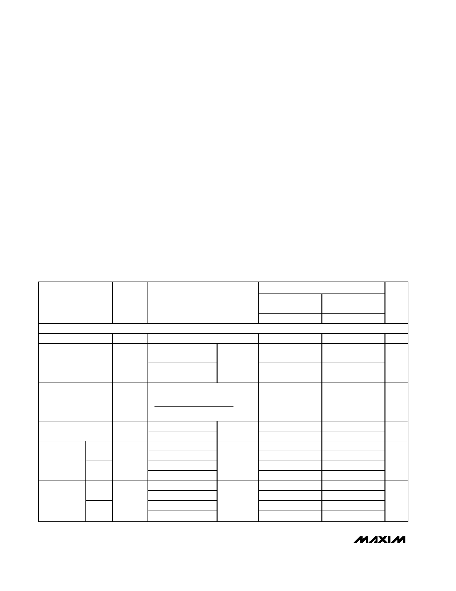
Ordering Information
MAX328
V+
V-
GND
A
0
A
1
A
2
EN
S1
S8
D
OP
AMP
+15V
-15V
40k
1/2W
40k
1/2W
ANALOG
INPUT
ANALOG
INPUT
DM7493
+15V
+15V
N.C.
CLK IN
N.C.
GND
V
02
V
01
AIN
BIN
Q
B
Q
C
Q
O
Q
A
V+
EN IN
(MUX ON/OFF CONTROL)
OUT
i BIAS < 1pA
1-OF-8 CHANNEL SEQUENTIAL MUX WITH 120V AC FAULT CAPABILITY
Typical Operating Circuit
19-1006; Rev 2; 9/01
For pricing, delivery, and ordering information, please contact Maxim/Dallas Direct! at
1-888-629-4642, or visit Maxim's website at www.maxim-ic.com.
*Contact factory for dice specifications.
**Contact factory for availability. Substrate may be allowed to
float or be connected to V+.
Ordering Information and Pin Configurations continued at
end of data sheet.
PART
TEMP RANGE
PIN-PACKAGE
MAX328CPE
0∞C to +70∞C
16 Plastic DIP
MAX328CWE
0∞C to +70∞C
16 Wide SO
MAX328CJE
0∞C to +70∞C
16 CERDIP
MAX328C/D
0∞C to +70∞C
Dice*
MAX328EGE
-40∞C to +85∞C
16 QFN
MAX328EPE
-40∞C to +85∞C
16 Plastic DIP
MAX328EWE
-40∞C to +85∞C
16 Wide SO
MAX328EJE
-40∞C to +85∞C
16 CERDIP**
MAX328MJE
-55∞C to +125∞C
16 CERDIP**
MAX328/MAX329
Ultra-Low Leakage Monolithic CMOS
Analog Multiplexers
2
_______________________________________________________________________________________
ABSOLUTE MAXIMUM RATINGS
ELECTRICAL CHARACTERISTICS
(V+ = +15V, V- = -15V, GND = 0V, T
A
= +25∞C, unless otherwise noted.)
Stresses beyond those listed under "Absolute Maximum Ratings" may cause permanent damage to the device. These are stress ratings only, and functional
operation of the device at these or any other conditions beyond those indicated in the operational sections of the specifications is not implied. Exposure to
absolute maximum rating conditions for extended periods may affect device reliability.
Voltage Referenced to V-
V+ ........................................................................................+44V
GND .....................................................................................+25V
Digital Inputs (Note 1), V
S
, V
D
............................-2V to (V+ + 2V)
Current (Any Terminal, Except S or D)................................30mA
Continuous Current, S or D
(pulsed at 1ms, 10% duty cycle max) ............................40mA
Operating Temperature Range
MAX328/329 C _ _ ..............................................0∞C to +70∞C
MAX328/329 E _ _ ...........................................-40∞C to +85∞C
MAX328/329 M _ _.........................................-55∞C to +125∞C
Power Dissipation (Package) (Note 1)
16-Pin CERDIP (Note 2) ...............................................900mW
16-Pin Plastic DIP (Note 3)...........................................470mW
16-Pin Wide SO (Note 4) ..............................................750mW
16-Pin QFN (Note 5) ...................................................1538mw
Storage Temperature.........................................-65∞C to +150∞C
LIMITS
MAX328M
MAX329M
MAX328C/E
MAX329C/E
PARAMETER
SYMBOL
TEST CONDITIONS
MIN
TYP
MAX
MIN
TYP
MAX
UNITS
SWITCH
Analog Signal Range
V
ANALOG
±15
±15
V
V
D
= 10V,
I
S
= 100µA
1.5
2.5
1.5
3.5
Drain-Source
On-Resistance
R
DS(ON)
V
D
= -10V,
I
S
= 100µA
Seq. each
switch on,
V
AL
= 0.8V,
V
AH
= 2.4V
1.0
2.5
1.0
3.5
k
Greatest Change in
Drain-Source On-
Resistance Between
Channels
R
DS(ON)
R
DS(on)
=
R
DS(ON)
Max - R
DS(ON)
Min
( )
R
DS(ON)
Ave
2
2
%
V
S
= 10V, V
D
= -10V
0.1
±10
0.1
±10
Source Off-Leakage
Current (Note 6)
I
S(OFF)
V
S
= -10V, V
D
= 10V
V
EN
= 0V
0.3
±10
0.3
±10
pA
V
D
= 10V, V
S
= -10V
0.3
±10
0.3
±10
MAX328
V
D
= -10V, V
S
= 10V
1.0
±10
1.0
±10
V
D
= 10V, V
S
= -10V
0.3
±10
0.3
±10
Drain Off-
Leakage
Current (Note 6) MAX329
I
D(OFF)
V
D
= -10V, V
S
= 10V
V
EN
= 0V
0.5
±10
0.5
±10
pA
V
S
(all) = V
D
= 10V
3.0
±10
3.0
±10
MAX328
V
S
(all) = V
D
= -10V
2.0
±10
2.0
±10
V
S
(all) = V
D
= 10V
1.5
±10
1.5
±10
Drain On-
Leakage
Current (Note 6) MAX329
I
D(ON)
V
S
(all) = V
D
= -10V
Seq. each
switch on,
V
AL
= 0.8V,
V
AH
= 2.4V
1.0
±10
1.0
±10
pA
Note 1: All leads soldered or welded to PC board.
Note 2: Derate 12mW/∞C above +75∞C.
Note 3: Derate 6.3mW/∞C above +75∞C.
Note 4: Derate 10mW/∞C above +75∞C.
Note 5: Derate 19.2mW/∞C above +75∞C.

MAX328/MAX329
Ultra-Low Leakage Monolithic CMOS
Analog Multiplexers
_______________________________________________________________________________________
3
ELECTRICAL CHARACTERISTICS (continued)
(V+ = +15V, V- = -15V, GND = 0V, T
A
= +25∞C, unless otherwise noted.)
LIMITS
MAX328M
MAX329M
MAX328C/E
MAX329C/E
PARAMETER
SYMBOL
TEST CONDITIONS
MIN
TYP
MAX
MIN
TYP
MAX
UNITS
INPUT
V
A
= 2.4V
0.001
±1
0.001
±1
Address Input Current,
Input Voltage High
I
AH
V
A
= 15V
0.001
±1
0.001
±1
µA
V
EN
= 2.4V
0.001
±1
0.001
±1
Address Input Current,
Input Voltage Low
I
AL
V
EN
= 0V
All
V
A
= 0V
0.001
±1
0.001
±1
µA
DYNAMIC
Switching Time of
Multiplexer
t
TRANSITION
See Figure 1
1.0
1.5
µs
Break-Before-Make
Interval
t
OPEN
See Figure 2
0.2
0.2
µs
Enable Turn-On Time
t
ON(EN)
See Figure 3
1.0
1.5
µs
Enable Turn-Off Time
t
OFF(EN)
See Figure 3
0.7
1.0
µs
Off-Isolation
OIRR
V
EN
= 0V, R
L
= 1k
, C
L
= 15pF,
V
S
= 7V
RMS
, f = 500kHz
84
84
dB
Source Off-Capacitance
C
S(OFF)
V
S
= 0V
V
EN
= 0V,
f = 1MHz
1.8
1.8
pF
MAX328
8.0
8.0
Drain Off-
Capacitance
MAX329
C
D(OFF)
V
D
= 0V
V
EN
= 0V,
f = 1MHz
4.0
4.0
pF
V
A
= +10V
1
1
V
A
= 0V
2
5
2
5
Charge Injection (Note 8)
Q
(INJ)
V
A
= -10V
4
4
pc
SUPPLY
Positive Supply Current
I+
V
EN
= 2.4V
V
A
= 0V/5V
4.5
200
4.5
200
µA
Negative Supply Current
I-
V
EN
= 2.4V
V
A
= 0V/5V
1
-100
1
-100
µA
Power-Supply Range for
Continuous Operation
(Note 7)
V
OP
±5
±18
±5
±18
V
Note 6: All leakage parameters are 100% tested at maximum rated operating temperature, i.e., +70∞C, +85∞C, +125∞C, and guaran-
teed by correlation at +25∞C.
Note 7: Electrical characteristics, such as On-Resistance, change when power supplies other than ±15V are used. Power-supply
range is a design characteristic, not production tested.
Note 8: Guaranteed by design.
Typical values are for DESIGN AID ONLY, not guaranteed or subject to production testing.
MAX328/MAX329
Ultra-Low Leakage Monolithic CMOS
Analog Multiplexers
4
_______________________________________________________________________________________
ELECTRICAL CHARACTERISTICS (Over Temperature)
(V+ = +15V, V- = -15V, GND = 0V, T
A
= T
MIN
to T
MAX
, unless otherwise noted.)
LIMITS
MAX328M
MAX329M
MAX328C/E
MAX329C/E
PARAMETER
SYMBOL
TEST CONDITIONS
MIN
TYP
MAX
MIN
TYP
MAX
UNITS
SWITCH
Analog Signal Range
V
ANALOG
±15
±15
V
V
D
= 10V,
I
S
= 100µA
2.2
4
1.9
5
Drain-Source
On-Resistance
R
DS(ON)
V
D
= -10V,
I
S
= 100µA
Seq. each
switch on,
V
AL
= 0.8V,
V
AH
= 2.4V
1.5
4
1.2
5
k
V
S
= 10V, V
D
= -10V
±5
±5
Source Off-
Leakage Current (Note 9)
I
S(OFF)
V
S
= -10V, V
D
= 10V
V
EN
= 0V
±5
±5
nA
V
D
= 10V, V
S
= -10V
±20
±20
MAX328
V
D
= -10V, V
S
= 10V
±20
±20
V
D
= 10V, V
S
= -10V
±10
±10
Drain Off-
Leakage
Current (Note 9) MAX329
I
D(OFF)
V
D
= -10V, V
S
= 10V
V
EN
= 0V
±10
±10
nA
V
S
(all) = V
D
= 10V
±20
±20
MAX328
V
S
(all) = V
D
= -10V
±20
±20
V
S
(all) = V
D
= 10V
±10
±10
Drain On-
Leakage
Current (Note 9) MAX329
I
D(ON)
V
S
(all) = V
D
= -10V
Seq. each
switch on,
V
AL
= 0.8V,
V
AH
= 2.4V
±10
±10
nA
INPUT
V
A
= 2.4V
0.01
±1
0.01
±1
Address Input Current,
Input Voltage High
I
AH
V
A
= 15V
0.01
±1
0.01
±1
µA
V
EN
= 2.4V
0.01
±1
0.01
±1
Address Input Current,
Input Voltage Low
I
AL
V
EN
= 0V
All
V
A
= 0V
0.01
±1
0.01
±1
µA
Note 9: Leakage parameters are 100% tested at maximum rated operating temperature, i.e., +70∞C, etc.

MAX328/MAX329
Ultra-Low Leakage Monolithic CMOS
Analog Multiplexers
_______________________________________________________________________________________
5
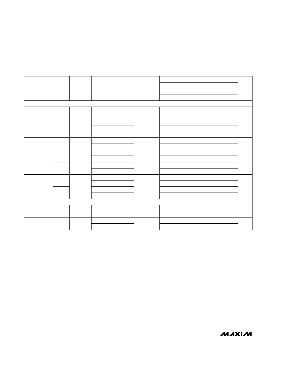
Typical Operating Characteristics
(T
A
= +25∞C, unless otherwise noted.)
R
DS(ON)
vs. ANALOG INPUT
FOR DUAL SUPPLIES
MAX328/MAX329 toc01
ANALOG INPUT (V)
R
DS(ON)
(k
)
10
5
0
-5
-10
1
2
3
4
5
6
7
8
9
0
-15
15
±5V SUPPLIES
±15V SUPPLIES
R
DS(ON)
vs. ANALOG INPUT
FOR SINGLE SUPPLY
MAX328/MAX329 toc02
ANALOG INPUT (V)
R
DS(ON)
(k
)
10
5
1
2
3
4
5
0
0
15
WITH +15V SUPPLY
I
S(OFF)
vs. TEMPERATURE
MAX328/MAX329 toc03
TEMPERATURE (
∞C)
LEAKAGE (nA)
105
85
65
45
25
5
-15
-35
0.001
0.01
0.1
1.0
10.0
0.0001
-55
125
V+ = 15V
V- = 15V
MAX328/
MAX329
I
D(ON),
I
D(OFF)
vs. TEMPERATURE
MAX328/MAX329 toc04
TEMPERATURE (
∞C)
LEAKAGE (nA)
105
85
65
45
25
5
-15
-35
0.01
0.1
1.0
10
100
0.001
-55
125
V+ = 15V
V- = 15V
MAX328