 | –≠–ª–µ–∫—Ç—Ä–æ–Ω–Ω—ã–π –∫–æ–º–ø–æ–Ω–µ–Ω—Ç: MAX338EJE | –°–∫–∞—á–∞—Ç—å:  PDF PDF  ZIP ZIP |

_______________General Description
The MAX338/MAX339 are monolithic, CMOS analog
multiplexers (muxes). The 8-channel MAX338 is
designed to connect one of eight inputs to a common
output by control of a 3-bit binary address. The dual, 4-
channel MAX339 is designed to connect one of four
inputs to a common output by control of a 2-bit binary
address. Both devices can be used as either a mux or
a demux. On-resistance is 400
max, and the devices
conduct current equally well in both directions.
These muxes feature extremely low off leakages (less
than 20pA at +25∞C), and extremely low on-channel
leakages (less than 50pA at +25∞C). The new design
offers guaranteed low charge injection (1.5pC typ) and
electrostatic discharge (ESD) protection greater than
2000V, per method 3015.7. These improved muxes are
pin-compatible upgrades for the industry-standard
DG508A and DG509A. For similar Maxim devices with
lower leakage and charge injection but higher on-resis-
tance, see the MAX328 and MAX329.
The MAX338/MAX339 operate from a single +4.5V to
+30V supply or from dual supplies of ±4.5V to ±20V.
All control inputs (whether address or enable) are TTL
compatible (+0.8V to +2.4V) over the full specified tem-
perature range and over the ±4.5V to ±18V supply
range. These parts are fabricated with Maxim's 44V sili-
con-gate process.
________________________Applications
Data-Acquisition Systems
Sample-and-Hold Circuits
Test Equipment
Heads-Up Displays
Military Radios
Communications Systems
Guidance and Control Systems
PBX, PABX
____________________________Features
o On-Resistance, <400 max
o Transition Time, <500ns
o On-Resistance Match, <10
o NO-Off Leakage Current, <20pA at +25∞C
o 1.5pC Charge Injection
o Single-Supply Operation (+4.5V to +30V)
Bipolar-Supply Operation (±4.5V to ±20V)
o Plug-In Upgrade for Industry-Standard
DG508A/DG509A
o Rail-to-Rail Signal Handling
o TTL/CMOS-Logic Compatible
o ESD Protection >2000V, per Method 3015.7
______________Ordering Information
MAX338/MAX339
8-Channel/Dual 4-Channel,
Low-Leakage, CMOS Analog Multiplexers
________________________________________________________________ Maxim Integrated Products
1
CMOS DECODE LOGIC
A2
A1
A0
EN
NO8
NO7
NO6
NO5
NO4
NO3
NO2
NO1
COM
V+
V-
GND
MAX338 8-CHANNEL SINGLE-ENDED MULTIPLEXER
16
15
14
13
12
11
10
9
1
2
3
4
5
6
7
8
A1
A2
GND
V+
NO1
V-
EN
A0
TOP VIEW
MAX338
NO5
NO6
NO7
NO8
COM
NO4
NO3
NO2
DIP/SO
Continued at end of data sheet.
_____________________Pin Configurations/Functional Diagrams/Truth Tables
19-0272; Rev 1; 9/01
PART
MAX338CPE
MAX338CSE
MAX338C/D
0∞C to +70∞C
0∞C to +70∞C
0∞C to +70∞C
TEMP. RANGE
PIN-PACKAGE
16 Plastic DIP
16 Narrow SO
Dice*
Ordering Information continued at end of data sheet.
* Contact factory for dice specifications.
** Contact factory for availability.
MAX338EPE
-40∞C to +85∞C
16 Plastic DIP
MAX338ESE
-40∞C to +85∞C
16 Narrow SO
MAX338EJE
-40∞C to +85∞C
16 CERDIP
MAX338MJE
-55∞C to +125∞C
16 CERDIP**
For pricing, delivery, and ordering information, please contact Maxim/Dallas Direct! at
1-888-629-4642, or visit Maxim's website at www.maxim-ic.com.
MAX338EGE
-40∞C to +85∞C
16 QFN

1.5
5
T
A
= +25∞C
MAX338/MAX339
8-Channel/Dual 4-Channel,
Low-Leakage, CMOS Analog Multiplexers
2
_______________________________________________________________________________________
ABSOLUTE MAXIMUM RATINGS
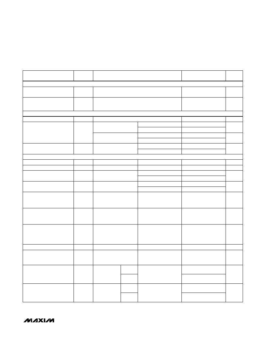
ELECTRICAL CHARACTERISTICS--Dual Supplies
(V+ = +15V, V- = -15V, GND = 0V, V
AH
= +2.4V, V
AL
= +0.8V, T
A
= T
MIN
to T
MAX
, unless otherwise noted.)
Stresses beyond those listed under "Absolute Maximum Ratings" may cause permanent damage to the device. These are stress ratings only, and functional
operation of the device at these or any other conditions beyond those indicated in the operational sections of the specifications is not implied. Exposure to
absolute maximum rating conditions for extended periods may affect device reliability.
Voltage Referenced to V-
V+ ............................................................................-0.3V, 44V
GND .........................................................................-0.3V, 25V
Digital Inputs, NO, COM (Note 1)...........(V- - 2V) to (V+ + 2V) or
30mA (whichever occurs first)
Continuous Current (any terminal) ......................................30mA
Peak Current, NO or COM
(pulsed at 1ms, 10% duty cycle max) ..........................100mA
Continuous Power Dissipation (TA = +70∞C)
Plastic DIP (derate 10.53mW/∞C above +70∞C) ..........842mW
Narrow SO (derate 8.70mW/∞C above +70∞C) ............696mW
QFN (derate 19.2mW/∞C above +70∞C) ....................1538mW
CERDIP (derate 10.00mW/∞C above +70∞C) ...............800mW
Operating Temperature Ranges
MAX33_C__ ........................................................0∞C to +70∞C
MAX33_E__......................................................-40∞C to +85∞C
MAX33_MJE ..................................................-55∞C to +125∞C
Storage Temperature Range .............................-65∞C to +150∞C
Lead Temperature (soldering, 10sec) .............................+300∞C
V
COM
= ±10V,
V
NO
= ±10V,
sequence
each switch
on
V
NO
= +10V,
V
COM
= ±10V,
V
EN
= 0V
V
COM
= +10V,
V
NO
= ±10V,
V
EN
= 0V
I
NO
= 0.2mA,
V
COM
= ±10V
V
NO
= ±10V,
V
COM
= +10V,
V
EN
= 0V
CONDITIONS
nA
-20
20
I
COM(ON)
COM-On Leakage Current
(Note 5)
-1.65
1.65
-0.05
0.008
0.05
-40
40
-3.25
3.25
-0.05
0.006
0.05
nA
-20
20
I
COM(OFF)
COM-Off Leakage Current
(Note 5)
-1.65
1.65
-0.05
0.005
0.05
-40
40
220
400
-3.25
3.25
-0.05
0.005
0.05
nA
-20
20
I
NO(OFF)
NO-Off Leakage Current
(Note 5)
-1.25
1.25
500
R
ON
On-Resistance
UNITS
MIN
TYP
MAX
(Note 2)
SYMBOL
PARAMETER
Note 1:
Signals on NO, COM, EN, A0, A1, or A2 exceeding V+ or V- are clamped by internal diodes. Limit forward current to
maximum current ratings.
V
-15
15
V
NO
,
V
COM
Analog Signal Range
I
NO
= 0.2mA,
V
COM
= ±10V (Note 4)
4
10
R
ON
On-Resistance Matching
Between Channels
(Note 3)
T
A
= +25∞C
T
A
= T
MIN
to T
MAX
T
A
= +25∞C
-0.02
0.001
0.02
T
A
= +25∞C
T
A
= T
MIN
to T
MAX
T
A
= +25∞C
T
A
= T
MIN
to T
MAX
T
A
= +25∞C
T
A
= T
MIN
to T
MAX
T
A
= +25∞C
T
A
= T
MIN
to T
MAX
T
A
= +25∞C
T
A
= T
MIN
to T
MAX
MAX339
MAX338
MAX339
MAX338
C, E
M
C, E
M
C, E
M
C, E
M
C, E
M
SWITCH
T
A
= T
MIN
to T
MAX
15
MAX338/MAX339
8-Channel/Dual 4-Channel,
Low-Leakage, CMOS Analog Multiplexers
_______________________________________________________________________________________
3
ELECTRICAL CHARACTERISTICS--Dual Supplies (continued)
(V+ = +15V, V- = -15V, GND = 0V, V
AH
= +2.4V, V
AL
= +0.8V, T
A
= T
MIN
to T
MAX
, unless otherwise noted.)
Off Isolation
(Note 6)
dB
-75
V
ISO
1.5
5
Q
Charge Injection
(Note 3)
100
500
ns
750
t
ON(EN)
Enable Turn-On Time
160
500
ns
10
140
t
OPEN
Break-Before-Make Interval
µA
-1.0
1.0
I
AL
Input Current with
Input Voltage Low
µA
-1.0
0.001
1.0
I
AH
Input Current with
Input Voltage High
µA
-10
10
I-
Negative Supply Current
-1
1
µA
600
I+
Positive Supply Current
290
500
V
±4.5
±20
Power-Supply Range
50
100
µA
150
UNITS
MIN
TYP
MAX
(Note 2)
SYMBOL
PARAMETER
Crosstalk Between Channels
V
CT
-92
dB
Logic Input Capacitance
C
IN
2
pF
NO-Off Capacitance
C
NO(OFF)
3
pF
11
COM-Off Capacitance
C
COM(OFF)
f = 1MHz,
V
EN
= 0.8V,
V
COM
= 0V,
Figure 8
6
pF
16
COM-On Capacitance
C
COM(ON)
f = 1MHz,
V
EN
= 2.4V,
V
COM
= 0V,
Figure 8
9
pF
T
A
= +25∞C
V
EN
= 0V or 2.4V,
V
A
= 0V
T
A
= +25∞C
V
A
= 2.4V or 15V
T
A
= +25∞C
T
A
= T
MIN
to T
MAX
T
A
= T
MIN
to T
MAX
T
A
= +25∞C
T
A
= +25∞C
T
A
= +25∞C
T
A
= T
MIN
to T
MAX
T
A
= +25∞C
T
A
= +25∞C
T
A
= T
MIN
to T
MAX
CONDITIONS
T
A
= +25∞C
T
A
= +25∞C
T
A
= +25∞C
T
A
= +25∞C
T
A
= +25∞C
V
EN
= 0V,
R
L
= 1k
,
f = 100kHz
C
L
= 100pF,
V
NO
= 0V,
R
S
= 0
, Figure 6
Figure 3
V
EN
= 0V or 2.4V,
V
A(ALL)
= 0V, 2.4V or 5V
Figure 4
V
EN
= 2.4V,
V
A(ALL)
= 2.4V
V
EN
= V
A
= 0V
V
EN
= 2.4V,
f = 100kHz,
V
GEN
= 1V
P-P
,
R
L
= 1k
, Figure 7
f = 1MHz
f = 1MHz,
V
EN
= V
NO
= 0V,
Figure 8
MAX338
MAX339
MAX338
MAX339
ns
200
500
t
TRANS
Transistion Time
T
A
= +25∞C
Figure 2
pC
ns
750
t
OFF(EN)
Enable Turn-Off Time
T
A
= T
MIN
to T
MAX
Figure 3
INPUT
SUPPLY
DYNAMIC

MAX338/MAX339
8-Channel/Dual 4-Channel,
Low-Leakage, CMOS Analog Multiplexers
4
_______________________________________________________________________________________
(Note 3)
CONDITIONS
C
L
= 100pF,
V
NO
= 0V,
R
S
= 0
V
INH
= 2.4V,
V
INL
= 0V,
V
NO1
= 5V,
Figure 3
V
INH
= 2.4V,
V
INL
= 0V,
V
NO1
= 5V,
Figure 3
V
NO1
= 8V,
V
NO8
= 0V,
V
IN
= 2.4V,
Figure 1
I
NO
= 0.2mA
V
COM
= 3V or 10V
pC
1.8
5
Q
Charge Injection
(Note 3)
ns
110
500
t
OFF(EN)
Enable Turn-Off Time
(Note 3)
V
0
12
V
NO
,
V
COM
Analog Signal Range
ns
280
500
t
ON(EN)
Enable Turn-On Time
(Note 3)
ns
210
500
t
TRANS
Transition Time
(Note 3)
460
650
R
ON
On-Resistance
UNITS
MIN
TYP
MAX
(Note 2)
SYMBOL
PARAMETER
ELECTRICAL CHARACTERISTICS--Single Supply
(V+ = +12V, V- = 0V, GND = 0V, V
AH
= +2.4V, V
AL
= +0.8V, T
A
= T
MIN
to T
MAX
, unless otherwise noted.)
Note 2: The algebraic convention where the most negative value is a minimum and the most positive value a maximum is used in
this data sheet.
Note 3: Guaranteed by design.
Note 4:
R
ON
= R
ON(MAX)
- R
ON(MIN).
Note 5: Leakage parameters are 100% tested at the maximum rated hot temperature and guaranteed by correlation at +25∞C.
Note 6: Worst-case isolation is on channel 4 because of its proximity to the drain pin. Off isolation = 20log V
COM
/V
NO
, where
V
COM
= output and V
NO
= input to off switch.
T
A
= +25∞C
T
A
= +25∞C
T
A
= +25∞C
T
A
= +25∞C
T
A
= +25∞C
SWITCH
DYNAMIC

MAX338/MAX339
8-Channel/Dual 4-Channel,
Low-Leakage, CMOS Analog Multiplexers
_______________________________________________________________________________________
5
600
ON-RESISTANCE vs. V
COM
(DUAL SUPPLIES)
500
MAX338/9 TOC-01
0
100
200
300
-20
20
-15
15
-10
10
-5
5
0
400
V
COM
(V)
±5V
±10V
±15V
±20V
R
ON
(
)
ON-RESISTANCE vs. V
COM
OVER
TEMPERATURE (DUAL SUPPLIES)
MAX338/9 TOC-02
0
100
200
300
-15
15
-10
10
-5
5
0
400
V
COM
(V)
+125∞C
+85∞C
+25∞C
-55∞C
R
ON
(
)
V+ = +15V
V- = -15V
1200
1400
ON-RESISTANCE vs. V
COM
(SINGLE SUPPLY)
1000
MAX338/9 TOC-03
0
200
400
600
15
20
10
5
0
800
V
COM
(V)
R
ON
(
)
+5V
+12V
+15V
+20V
600
700
ON-RESISTANCE vs. V
COM
OVER
TEMPERATURE (SINGLE SUPPLY)
500
MAX338/9 TOC-04
0
100
200
300
15
10
5
0
400
V
COM
(V)
R
ON
(
)
+125∞C
+85∞C
+25∞C
-55∞C
V+ = +15V
V- = 0V
30
CHARGE INJECTION vs. V
COM
20
MAX338/9 TOC-07
-30
-20
-10
0
-15
15
-10
10
-5
5
0
10
V
COM
(V)
Q
j
(pC)
C
L
= 100pF
V- = 0V
±15V
40
+12V
+5V
10
0.0001
-55
125
OFF LEAKAGE vs. TEMPERATURE
1
MAX338/9 TOC-05
TEMPERATURE (
∞C)
OFF LEAKAGE (nA)
25
0.01
0.001
-35 -15
65
0.1
100
1000
45
85 105
5
I
NO (OFF)
I
COM (OFF)
V+ = +15V
V- = -15V
10
0.0001
-55
125
ON LEAKAGE vs. TEMPERATURE
1
MAX338/9 TOC-06
TEMPERATURE (
∞C)
ON LEAKAGE (nA)
25
0.01
0.001
-35 -15
65
0.1
100
1000
45
85 105
5
I
COM (ON)
V+ = +15V
V- = -15V
100
0.001
-55
125
SUPPLY CURRENT vs. TEMPERATURE
10
MAX338/9 TOC-08
TEMPERATURE (
∞C)
I+, I- (
µ
A)
25
0.1
0.01
-35 -15
65
1
45
85 105
5
I-
1000
I+, V
A(ALL)
= 2.4V
I+, V
A
= 0V
600
1000
900
800
700
TRANSITION TIME vs.
POWER SUPPLIES
500
MAX338/9 TOC-09
0
100
200
300
±15
±20
±10
OR 10V
(SINGLE)
±5
OR 5V
(SINGLE)
0
400
SUPPLY VOLTAGE (V)
t
TRANS
(nS)
SINGLE SUPPLY
DUAL SUPPLIES
R
L
= 1k
__________________________________________Typical Operating Characteristics
(T
A
= +25∞C, unless otherwise noted.)