 | –≠–ª–µ–∫—Ç—Ä–æ–Ω–Ω—ã–π –∫–æ–º–ø–æ–Ω–µ–Ω—Ç: MAX354 | –°–∫–∞—á–∞—Ç—å:  PDF PDF  ZIP ZIP |

_______________General Description
The MAX354/MAX355 fault-protected multiplexers
(muxes) use a series N-channel, P-channel, N-channel
structure that protects the devices from overvoltage up
to 40V beyond the supply rails during power-up, power-
down, and fault conditions. The MAX354/MAX355 also
protect sensitive circuit components against voltages
near or beyond the normal supplies.
The MAX354 single 8-channel mux and the MAX355
dual 4-channel mux protect analog signals while oper-
ating from a single 4.5V to 36V supply or ±4.5V to ±18V
dual supplies. These muxes have 350
on-resistance
and can be used for demultiplexing as well as multi-
plexing. Input leakage current is less than 0.5nA at
+25∞C and less than 5nA at +85∞C.
All digital inputs have 0.8V and 2.4V logic thresholds,
ensuring both TTL and CMOS logic compatibility with-
out pull-up resistors. Break-before-make operation is
guaranteed and power consumption is less than
1.5mW.
________________________Applications
Data-Acquisition Systems
Industrial and Process Control
Avionics
ATE Equipment
Signal Routing
Redundant/Backup Systems
____________________________Features
o
350
Max On-Resistance
o
Improved 2nd Source for MAX358/MAX359 and
DG458/DG459
o
Pin Compatible with ADG508F/ADG509F
o
All Switches Off with Supplies Off
o
On Switch Turns Off with Overvoltage
o
Output Clamps at 1.5V Below Supply Rails
o
0.5nA Max Input Leakage at +25∞C (5nA at +85∞C)
o
No Power-Up Sequencing Required
o
TTL and CMOS-Logic Compatibility
______________Ordering Information
* Dice are tested at T
A
= +25∞C only.
** Contact factory for availability.
________________________________________________________________
Maxim Integrated Products
1
16
15
14
13
12
11
10
9
1
2
3
4
5
6
7
8
A1
A2
GND
V+
NO1
V-
EN
A0
TOP VIEW
MAX354
NO5
NO6
NO7
NO8
COM
NO4
NO3
NO2
DIP/SO
LOGIC
16
15
14
13
12
11
10
9
1
2
3
4
5
6
7
8
A1
GND
V+
NO1B
NO1A
V-
EN
A0
MAX355
NO2B
NO3B
NO4B
COMB
COMA
NO4A
NO3A
NO2A
DIP/SO
LOGIC
__________________________________________________________Pin Configurations
For free samples & the latest literature: http://www.maxim-ic.com, or phone 1-800-998-8800
PART
MAX354
CPE
MAX354CWE
MAX354C/D
0∞C to +70∞C
0∞C to +70∞C
0∞C to +70∞C
TEMP. RANGE
PIN-PACKAGE
16 Plastic DIP
16 Wide SO
Dice*
MAX354EPE
MAX354EWE
-40∞C to +85∞C
-40∞C to +85∞C
16 Plastic DIP
16 Wide SO
MAX354MJE
-55∞C to +125∞C
16 CERDIP**
19-0389; Rev. 2; 9/96
MAX355
CPE
MAX355CWE
MAX355C/D
0∞C to +70∞C
0∞C to +70∞C
0∞C to +70∞C
16 Plastic DIP
16 Wide SO
Dice*
MAX355EPE
MAX355EWE
-40∞C to +85∞C
-40∞C to +85∞C
16 Plastic DIP
16 Wide SO
MAX355MJE
-55∞C to +125∞C
16 CERDIP**
MAX354/MAX355
Fault-Protected Analog Multiplexers

MAX354/MAX355
Fault-Protected Analog Multiplexers
2
_______________________________________________________________________________________
ABSOLUTE MAXIMUM RATINGS
ELECTRICAL CHARACTERISTICS
(V+ = +15V, V- = -15V, GND = 0V, V
AH
= V
ENH
= 2.4V, V
AL
= V
ENL
= 0.8V, T
A
= T
MIN
to T
MAX
, unless otherwise noted.)
Stresses beyond those listed under "Absolute Maximum Ratings" may cause permanent damage to the device. These are stress ratings only, and functional
operation of the device at these or any other conditions beyond those indicated in the operational sections of the specifications is not implied. Exposure to
absolute maximum rating conditions for extended periods may affect device reliability.
(Voltages referenced to GND, unless otherwise noted.)
V+ ...........................................................................-0.3V to +44V
V- ............................................................................+0.3V to -44V
V+ to V-...................................................................-0.3V to +44V
Digital Inputs.........................................(V+ + 0.3V) to (V- - 0.3V)
Input Overvoltage with Mux Power On
V+ = +15V ....................................................................... +25V
V- = -15V ............................................................................-25V
Input Overvoltage with Mux Power Off
V+ = 0V.............................................................................+40V
V- = 0V ...............................................................................-40V
Continuous Current into Any Terminal .............................±30mA
Peak Current into Any Terminal ........................................±50mA
Continuous Power Dissipation (T
A
= +70∞C)
Plastic DIP (derate 10.53mW/∞C above +70∞C) ...........842mW
Wide SO (derate 9.52mW/∞C above +70∞C)................ 762mW
CERDIP (derate 10.00mW/∞C above +70∞C) ...............800mW
Operating Temperature Ranges
MAX35_C_ _ ........................................................0∞C to +70∞C
MAX35_E_ _......................................................-40∞C to +85∞C
MAX35_M_ _ ...................................................-55∞C to +125∞C
Storage Temperature Range .............................-65∞C to +150∞C
Lead Temperature (soldering, 10sec) ............................ +300∞C
V
COM
= ±10V,
V
NO
= ±10V,
V
EN
= 0V
V
COM
= ±10V,
V
NO
= ±10V,
V
EN
= 0V
CONDITIONS
-50
50
I
COM(OFF)
COM-Off Leakage Current
(Note 4)
-15
15
-0.5
0.02
0.5
-100
100
-25
25
nA
-0.5
0.02
0.5
V
(V+ - 40)
(V- + 40)
V
COM
, V
NO
Analog Signal Range
500
R
ON
On-Resistance
(Note 2)
450
285
350
UNITS
MIN
TYP
MAX
SYMBOL
PARAMETER
T
A
= T
MIN
to T
MAX
T
A
= T
MIN
to T
MAX
T
A
= T
MIN
to T
MAX
MAX355
I
NO
= 1.0mA, V
COM
= ±10V
MAX354
(Note 1)
M
C, E
M
C, E
T
A
= +25∞C
M
T
A
= +25∞C
C, E
T
A
= +25∞C
V
COM
= ±10V,
V
NO
= ±10V,
sequence each
switch on
-100
100
I
COM(ON)
COM-On Leakage Current
(Note 4)
-15
15
-0.5
0.02
0.5
-200
200
-30
30
nA
-0.5
0.02
0.5
T
A
= T
MIN
to T
MAX
T
A
= T
MIN
to T
MAX
MAX355
MAX354
M
C, E
T
A
= +25∞C
M
C, E
T
A
= +25∞C
-12
12
Fault-Free Analog
Signal Range
V+ = +15V, V- = -15V (Note 1)
7
12
-50
50
I
NO(OFF)
NO-Off Leakage Current
(Note 4)
-5.0
5.0
nA
-0.5
0.01
0.5
15
R
ON
On-Resistance Matching
Between Channels
T
A
= T
MIN
to T
MAX
V
COM
= ±10V,
V
NO
= ±10V,
V
EN
= 0V
I
NO
= 1.0mA, V
COM
= ±10V
(Note 3)
T
A
= +25∞C
M
C, E
T
A
= +25∞C
T
A
= T
MIN
to T
MAX
SWITCH
±
±
±
V

pF
V
EN
= V
A
= 0V
MAX354/MAX355
Fault-Protected Analog Multiplexers
_______________________________________________________________________________________
3
CONDITIONS
pF
1.6
C
NO(OFF)
NO-Off Capacitance
V
CT
Crosstalk Between Channels
dB
92
ns
50
100
t
OPEN
Break-Before-Make Interval
ns
400
t
ON(EN)
Enable Turn-On Time
160
250
nA
-5
0.01
5
Output Leakage Current
(with Overvoltage)
ns
180
250
t
TRANS
Transition Time
V
±4.5
±18
Power-Supply Range
µA
-300
300
I+
Positive Supply Current
µA
-1
1
I-
Negative Supply Current
UNITS
MIN
TYP
MAX
SYMBOL
PARAMETER
f = 1MHz, V
EN
= V
D
= 0V
V
EN
= 2.4V, f = 100kHz,
V
GEN
= 1V
p-p
, R
L
= 1k
,
Figure 6
Figure1
Figure 3
Figure 2
V
D
= 0V,
analog overvoltage = ±33V
T
A
= +25∞C
T
A
= +25∞C
T
A
= +25∞C
T
A
= +25∞C
T
A
= +25∞C
T
A
= +25∞C
T
A
= T
MIN
to T
MAX
T
A
= +25∞C
ELECTRICAL CHARACTERISTICS (continued)
(V+ = +15V, V- = -15V, GND = 0V, V
AH
= V
ENH
= 2.4V, V
AL
= V
ENL
= 0.8V, T
A
= T
MIN
to T
MAX
, unless otherwise noted.)
T
A
= +25∞C
µA
V
A
= V
EN
= 0.8V
V
A
= V
EN
= 2.4V
µA
-1
1
I
A_H
, I
ENH
Input Current with
Input Voltage High
-1
1
I
A_L
, I
ENL
Input Current with
Input Voltage Low
V
EN
= V
A
= 5V
ns
300
t
OFF(EN)
Enable Turn-Off Time
80
200
Figure 2
T
A
= T
MIN
to T
MAX
T
A
= +25∞C
V
T
A
= T
MIN
to T
MAX
T
A
= T
MIN
to T
MAX
V
2.4
V
A_H
, V
ENH
Logic High Input Voltage
0.8
V
A_L
, V
ENL
Logic Low Input Voltage
T
A
= T
MIN
to T
MAX
µA
-2
2
T
A
= +25∞C
T
A
= T
MIN
to T
MAX
µA
-2
2
-0.1
0.001
0.1
Input Leakage Current
(with Overvoltage)
V
IN
= ±25V, V
O
= ±10V
T
A
= +25∞C
T
A
= T
MIN
to T
MAX
µA
-2
2
-0.1
0.001
0.1
Input Leakage Current
(with Power Supplies Off)
V
IN
= ±25V, V
EN
= V
O
= 0V,
V
A0
= V
A1
= V
A2
= 0V or 5V
T
A
= +25∞C
T
A
= T
MIN
to T
MAX
T
A
= +25∞C
T
A
= T
MIN
to T
MAX
-5
5
-5
5
T
A
= T
MIN
to T
MAX
-500
500
T
A
= T
MIN
to T
MAX
-100
100
T
A
= T
MIN
to T
MAX
400
pC
80
V
CTE
Charge Injection
C
L
= 10nF, V
S
= 0V, R
S
= 0
,
Figure 4
T
A
= +25∞C
dB
100
V
ISO
Off Isolation
V
EN
= 0V, R
L
= 1k
, f = 100kHz,
Figure 5
T
A
= +25∞C
pF
2.5
C
IN
Logic Input Capacitance
f = 1MHz, Figure 7
T
A
= +25∞C
FAULT
SUPPLY
DYNAMIC
DIGITAL LOGIC INPUT
MAX354/MAX355
Fault-Protected Analog Multiplexers
4
_______________________________________________________________________________________
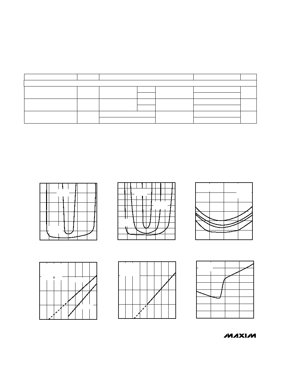
__________________________________________Typical Operating Characteristics
(T
A
= +25∞C, unless otherwise noted.)
100
10
0.0001
-15
15
ON-RESISTANCE vs. ANALOG VOLTAGE
1
MAX354/5-1a
ANALOG VOLTAGE (V)
R
ON
(M
)
0
0.01
0.001
-10
-5
10
0.1
5
V+ = +5V
V- = -5V
V+ = +15V
V- = -15V
2000
1600
1800
0
-15
15
ON-RESISTANCE vs. ANALOG VOLTAGE
800
1000
1200
1400
MAX354/5-1b
ANALOG VOLTAGE (V)
R
ON
(
)
0
400
200
-10
-5
10
600
5
V+ = +5V
V- = -5V
V+ = +15V
V- = -15V
V+ = +10V
V- = -10V
700
600
100
ON-RESISTANCE vs.
V
COM
AND TEMPERATURE
500
MAX354/5-2
V
COM
(V)
R
ON
(
)
0
300
200
-10
-5
10
400
5
A: +125∞C
B: +85∞C
C: +70∞C
D: +25∞C
V+ = +15V
V- = -15V
A
C
D
B
100
0.01
-75
75 100 125
OFF LEAKAGE vs. TEMPERATURE
10
MAX354-3
TEMPERATURE (∞C)
OFF LEAKAGE (nA)
0
0.1
-50
-25
50
1
25
V+ = +15V
V- = -15V
V
NO_
= ±10V
V
COM_
= 10V
I
COM(OFF)
I
NO(OFF)
100
0.01
-75
75 100 125
ON LEAKAGE vs. TEMPERATURE
10
MAX354-4
TEMPERATURE (∞C)
ON LEAKAGE (nA)
0
0.1
-50
-25
50
1
25
V+ = +15V
V- = -15V
V
COM_
= ±10V
200
-200
-10
5
10
CHARGE INJECTION vs. V
COM
100
150
MAX354-5
V
COM
(V)
Q
j
(pC)
-100
-150
-5
50
0
-50
0
V+ = +15V
V- = -15V
Note 1:
When the analog signal exceeds +13.5V or -13.5V, the blocking action of Maxim's gate structure goes into operation. Only
leakage currents flow, and the channel on-resistance rises to infinity (see
Typical Operating Characteristics).
Note 2:
Electrical characteristics such as on-resistance will change when power supplies other than ±15V are used.
Note 3:
R
ON
= R
ON(MAX)
- R
ON(MIN)
Note 4:
Leakage parameters are 100% tested at maximum rated hot operating temperature, and guaranteed by correlation at +25∞C.
Note 5:
Guaranteed by design.
ELECTRICAL CHARACTERISTICS (continued)
(V+ = +15V, V- = -15V, GND = 0V, V
AH
= V
ENH
= 2.4V, V
AL
= V
ENL
= 0.8V, T
A
= T
MIN
to T
MAX
, unless otherwise noted.)
f = 1MHz, Figure 7,
V
EN
= V
D
= 0V
f = 1MHz, Figure 7,
V
EN
= V
D
= 0V
CONDITIONS
14
C
COM(ON)
COM-On Capacitance
pF
28
5
C
COM(OFF)
COM-Off Capacitance
pF
11
0.1%
2.5
t
SETT
Setting Time (Note 5)
UNITS
MIN
TYP
MAX
SYMBOL
PARAMETER
MAX355
MAX354
MAX355
MAX354
µs
1
T
A
= +25∞C
0.01%
T
A
= +25∞C
T
A
= +25∞C
DYNAMIC (cont'd)

MAX354/MAX355
Fault-Protected Analog Multiplexers
_______________________________________________________________________________________
5
____________________________Typical Operating Characteristics (continued)
(T
A
= +25∞C, unless otherwise noted.)
______________________________________________________________Pin Description
1000
0.1
-75
75 100 125
SUPPLY CURRENT vs. TEMPERATURE
100
MAX354-6
TEMPERATURE (∞C)
I+, I- (
µ
A)
0
1
-50
-25
50
10
25
V+ = +15V
V- = -15V
V
EN
= +5V
I+ (V
A_
= 0V)
I-
I+ (V
A_
= 5V)
10m
10p
1n
-70
-10
10
30
50
70
FAULT CURRENT vs. FAULT VOLTAGE
1m
FAULT VOLTAGE (V)
FAULT CURRENT (A)
100p
-50
100
µ
10
µ
1
µ
100m
10n
-30
V+ = V- = 0V
V+ = +15V
V- = -15V
Ground
GND
15
14
Positive Supply Voltage Input
V+
14
13
Analog Inputs--bidirectional "B" switch
NO4B≠NO1B
10≠13
--
Analog Inputs--bidirectional
NO8≠NO5
--
9≠12
Analog Outputs--bidirectional
COMA, COMB
8, 9
--
Analog Output--bidirectional
COM
--
8
Analog Inputs--bidirectional "A" switch
NO1A≠NO4A
4≠7
--
Analog Inputs--bidirectional
NO1≠NO4
--
4≠7
Negative Supply Voltage Input. Connect to GND for single-supply operation.
V-
3
3
Enable Logic Input. See truth tables.
EN
2
2
Address Logic Inputs
A0, A1
--
--
Address Logic Inputs
A0, A2, A1
1, 15, 16
FUNCTION
NAME
MAX355
MAX354
PIN
1, 16
Note:
Analog inputs and outputs are electrically identical and completely interchangeable.