 | –≠–ª–µ–∫—Ç—Ä–æ–Ω–Ω—ã–π –∫–æ–º–ø–æ–Ω–µ–Ω—Ç: MAX379 | –°–∫–∞—á–∞—Ç—å:  PDF PDF  ZIP ZIP |
_______________General Description
The MAX378 8-channel single-ended (1-of-8) multiplexer
and the MAX379 4-channel differential (2-of-8) multiplexer
use a series N-channel/P-channel/N-channel structure to
provide significant fault protection. If the power supplies to
the MAX378/MAX379 are inadvertently turned off while
input voltages are still applied,
all channels in the muxes
are turned off, and only a few nanoamperes of leakage cur-
rent will flow into the inputs. This protects not only the
MAX378/MAX379 and the circuitry they drive, but also the
sensors or signal sources that drive the muxes.
The series N-channel/P-channel/N-channel protection
structure has two significant advantages over the simple
current-limiting protection scheme of the industry's first-
generation fault-protected muxes. First, the Maxim protec-
tion scheme limits fault currents to nanoamp leakage
values rather than many milliamperes. This prevents dam-
age to sensors or other sensitive signal sources. Second,
the MAX378/MAX379 fault-protected muxes can withstand
a
continuous ±60V input, unlike the first generation, which
had a continuous ±35V input limitation imposed by power
dissipation considerations.
All digital inputs have logic thresholds of 0.8V and 2.4V,
ensuring both TTL and CMOS compatibility without requir-
ing pull-up resistors. Break-before-make operation is
guaranteed. Power dissipation is less than 2mW.
________________________Applications
Data Acquisition Systems
Industrial and Process Control Systems
Avionics Test Equipment
Signal Routing Between Systems
____________________________Features
o
Fault Input Voltage ±75V with Power Supplies Off
o
Fault Input Voltage ±60V with ±15V Power Supplies
o
All Switches Off with Power Supplies Off
o
On Channel Turns OFF if Overvoltage Occurs on
Input or Output
o
Only Nanoamperes of Input Current Under All
Fault Conditions
o
No Increase in Supply Currents Due to Fault
Conditions
o
Latchup-Proof Construction
o
Operates from ±4.5V to ±18V Supplies
o
All Digital Inputs are TTL and CMOS Compatible
o
Low-Power Monolithic CMOS Design
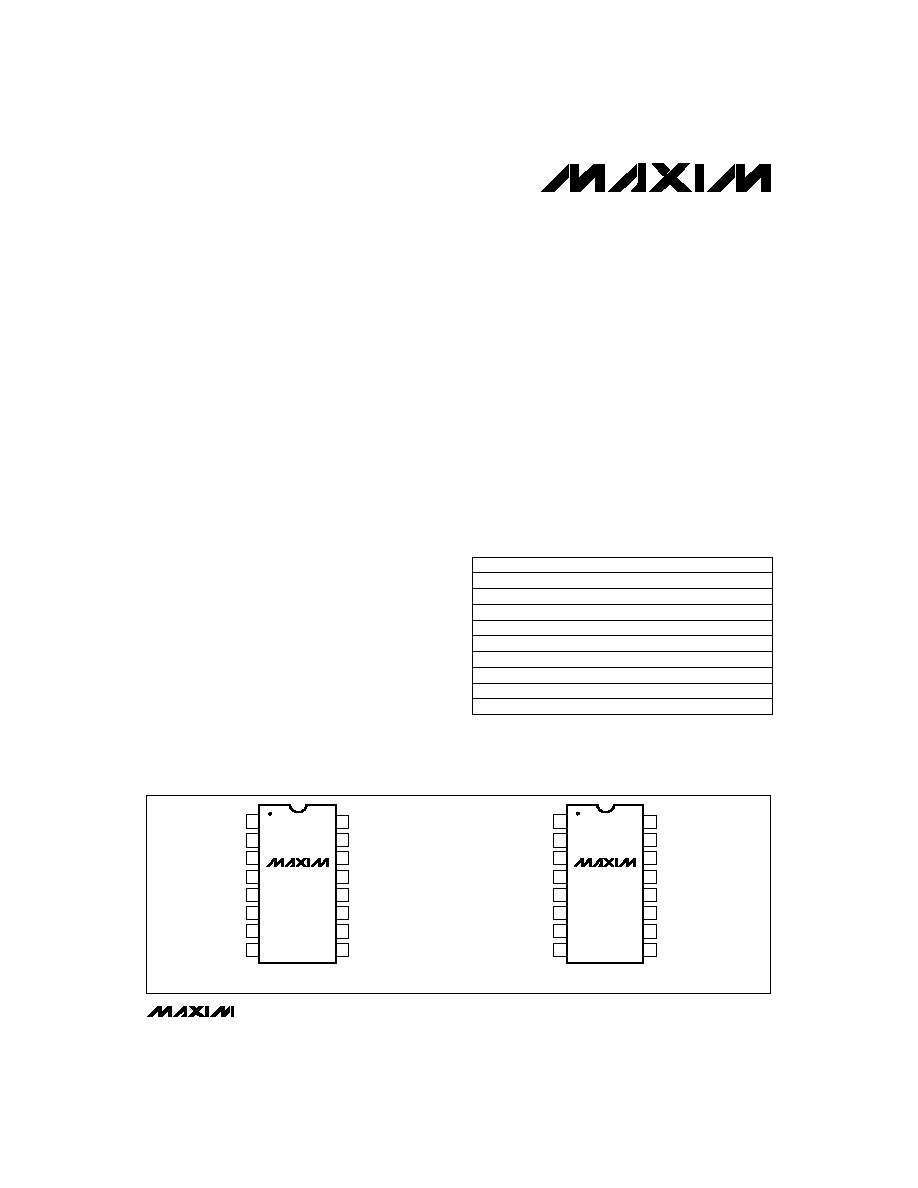
______________Ordering Information
Ordering Information continued at end of data sheet.
* Contact factory for availability.
**The substrate may be allowed to float or be tied to V+ (JI CMOS).
MAX378/MAX379
High-Voltage, Fault-Protected
Analog Multiplexers
________________________________________________________________
Maxim Integrated Products
1
16
15
14
13
12
11
10
9
1
2
3
4
5
6
7
8
A1
A2
GND
V+
IN1
V-
EN
A0
TOP VIEW
MAX378
IN5
IN6
IN7
IN8
OUT
IN4
IN3
IN2
DIP
16
15
14
13
12
11
10
9
1
2
3
4
5
6
7
8
A1
GND
V+
IN1B
IN1A
V-
EN
A0
MAX379
IN2B
IN3B
IN4B
OUTB
OUTA
IN4A
IN3A
IN2A
DIP
__________________________________________________________Pin Configurations
Call toll free 1-800-998-8800 for free samples or literature.
19-1902; Rev 1; 8/94
PART
MAX378
CPE
MAX378CWG
MAX378CJE
0∞C to +70∞C
0∞C to +70∞C
0∞C to +70∞C
TEMP. RANGE
PIN-PACKAGE
16 Plastic DIP
24 Wide SO
16 CERDIP
MAX378EPE
MAX378EWG
-40∞C to +85∞C
-40∞C to +85∞C
16 Plastic DIP
24 Wide SO
MAX378EJE
MAX378MJE
-55∞C to +125∞C
-40∞C to +85∞C
16 CERDIP
16 CERDIP
MAX378MLP
-55∞C to +125∞C
20 LCC*
Pin Configurations continued at end of data sheet.
MAX378C/D
0∞C to +70∞C
Dice**
MAX378/MAX379
High-Voltage, Fault-Protected
Analog Multiplexers
2
_______________________________________________________________________________________
ABSOLUTE MAXIMUM RATINGS
ELECTRICAL CHARACTERISTICS
(V+ = +15V, V- = -15V; V
AH
(Logic Level High) = +2.4V, V
AL
(Logic Level Low) = +0.8V, unless otherwise noted.)
Stresses beyond those listed under "Absolute Maximum Ratings" may cause permanent damage to the device. These are stress ratings only, and functional
operation of the device at these or any other conditions beyond those indicated in the operational sections of the specifications is not implied. Exposure to
absolute maximum rating conditions for extended periods may affect device reliability.
Voltage between Supply Pins ..............................................+44V
V+ to Ground ...................................................................+22V
V- to Ground......................................................................-22V
Digital Input Overvoltage:
V+......................................................................+4V
V- ........................................................................-4V
Analog Input with Multiplexer Power On..............................±65V
Recommended
V+ .....................................+15V
Power Supplies
V- .......................................-15V
Analog Input with Multiplexer Power Off..............................±80V
Continuous Current, IN or OUT...........................................20mA
Peak Current, IN or OUT
(Pulsed at 1ms, 10% duty cycle max) ............................40mA
Power Dissipation (Note 1) (CERDIP) ................................1.28W
Operating Temperature Range:
MAX378/379C .....................................................0∞C to +70∞C
MAX378/379E ..................................................-40∞C to +85∞C
MAX378/379M ...............................................-55∞C to +125∞C
Storage Temperature Range .............................-65∞C to +150∞C
(Note 4)
V
IN
= ±60V, V
OUT
= ±10V
(Notes 3, 4)
(Note 2)
MAX379 only
(Note 6)
V
A
= 5V or 0V (Note 5)
V
OUT
= 0V, V
IN
= ±60V
(Notes 3, 4)
(Note 4)
µA
-1.0
1.0
I
A
Input Leakage Current
(High or Low)
V
2.4
V
AH
Input High Threshold
-100
100
k
3.0
4.0
V
0.8
V
AL
Input Low Threshold
µA
25
I
IN(OFF)
Input Leakage Current
(with Overvoltage)
µA
10
V
-15
+15
V
AN
Analog Signal Range
nA
-50
50
I
DIFF
Differential OFF Output
Leakage Current
nA
20
I
OUT(OFF)
Output Leakage Current
(with Input Overvoltage)
V
EN
, V
A
{
{
}
Note 1:
Derate 12.8mW/∞C above T
A
= +75∞C
V
OUT
= ±10V, I
IN
= 100µA
V
AL
= 0.8V, V
AH
= 2.4V
2.0
3.0
r
DS(ON)
ON Resistance
Full
+25∞C
Full
Full
Full
+25∞C
Full
+25∞C
-1.0
1.0
2.4
-100
100
3.0
4.0
0.8
40
20
-15
+15
-50
50
20
2.0
3.5
nA
-50
50
V
IN
= ±10V, V
OUT
= 10V
V
EN
= 0.8V (Note 6)
-0.5
0.03
0.5
I
IN(OFF)
OFF Input Leakage Current
+25∞C
-50
50
-1.0
0.03
1.0
nA
-200
200
V
OUT
= ±10V, V
IN
= 10V
V
EN
= 0.8V
MAX378
(Note 6)
MAX379
-1.0
0.1
1.0
I
OUT(OFF)
OFF Output Leakage Current
+25∞C
-200
200
-2.0
0.1
2.0
nA
-600
600
V
IN(ALL)
= V
OUT
= ±10V
V
AH
= V
EN
= 2.4V
MAX378
V
AL
= 0.8V (Note 5)
MAX379
-10
0.1
10
I
OUT(ON)
ON Channel Leakage Current
+25∞C
-600
600
-20
0.1
20
-300
300
-300
300
V
IN
= ±75V, V
EN
= V
OUT
= 0V
A
0
= A
1
= A
2
= 0V or 5V
µA
10
I
IN(OFF)
Input Leakage Current
(with Power Supplies Off)
+25∞C
20
MIN TYP MAX
MIN TYP MAX
CONDITIONS
UNITS
-55∞C to +125∞C
SYMBOL
PARAMETER
TEMP
0∞C to +70∞C
and
-40∞C to +85∞C
STATIC
FAULT
CONTROL
±
±
Full
Full
Full
Full
Full
Full
Full

MAX378/MAX379
High-Voltage, Fault-Protected
Analog Multiplexers
_______________________________________________________________________________________
3
Note 2:
When the analog signal exceeds +13.5V or -12V, the blocking action of Maxim's gate structure goes into operation. Only
leakage currents flow and the channel ON resistance rises to infinity.
Note 3:
The value shown is the steady-state value. The transient leakage is typically 50µA. See
Detailed Description.
Note 4:
Guaranteed by other static parameters.
Note 5:
Digital input leakage is primarily due to the clamp diodes. Typical leakage is less than 1nA at +25∞C.
Note 6:
Leakage currents not tested at T
A
= cold temp.
Note 7:
Electrical characteristics, such as ON Resistance, will change when power supplies other than ±15V are used.
ELECTRICAL CHARACTERISTICS (continued)
(V+ = +15V, V- = -15V; V
AH
(Logic Level High) = +2.4V, V
AL
(Logic Level Low) = +0.8V, unless otherwise noted.)
pF
0.1
C
DS(OFF)
Input to Output Capacitance
V
EN
= 0.8V or 2.4V
All V
A
= 0V or 5V
+25∞C
V
EN
= 0.8V, R
L
= 1k
, C
L
= 15pF
V = 7V
RMS
, f = 100kHz
(Note 7)
MAX378
MAX379
CONDITIONS
0.1
V
±4.5
±18
V
OP
Power-Supply Range for
Continuous Operation
0.3
0.7
ns
1000
mA
0.1
0.6
I+
Positive Supply Current
pF
5
C
A
Digital Input Capacitance
12
dB
50
68
OFF
(ISO)
"OFF Isolation"
pF
5
C
IN(OFF)
Channel Input Capacitance
pF
25
C
OUT(OFF)
Channel Output Capacitance
UNITS
-55∞C to +125∞C
SYMBOL
PARAMETER
Figure 3
400
750
t
ON(EN)
Enable Delay (ON)
+25∞C
+25∞C
+25∞C
+25∞C
+25∞C
+25∞C
TEMP
+25∞C
±4.5
±18
0.5
1.0
1500
0.2
1.0
5
12
50
68
5
25
0∞C to +70∞C
and
-40∞C to +85∞C
400 1000
µs
3.5
1.2
t
SETT
Settling Time (0.1%)
(0.01%)
+25∞C
3.5
1.2
Figure 1
µs
0.5
1.0
t
A
Access Time
+25∞C
0.5
1.0
V
EN
= +5V, V
IN
= ±10V
A
0
, A
1
, A
2
strobed
ns
25
200
t
ON
-t
OFF
Break-Before-Make Delay
(Figure 2)
+25∞C
25
200
ns
1000
Figure 3
300
500
t
OFF(EN)
Enable Delay (OFF)
+25∞C
1000
300
V
EN
= 0.8V or 2.4V
All V
A
= 0V or 5V
0.02
0.2
mA
0.01
0.1
I-
Negative Supply Current
+25∞C
0.02
0.1
0.01
0.1
MIN TYP MAX
MIN TYP MAX
SUPPLY
DYNAMIC
Full
Full
Full
Full

MAX378/MAX379
High-Voltage, Fault-Protected
Analog Multiplexers
4
_______________________________________________________________________________________
1m
10p
-100
-50
50
100
INPUT LEAKAGE vs.
INPUT VOLTAGE WITH V+ = V- = 0V
1n
10
µ
MAX378-1
V
IN
(V)
INPUT CURRENT (A)
0
100n
100p
10n
100
µ
1
µ
-80V
+80V
OPERATING
RANGE
100
µ
1p
-120
-60
60
120
OFF CHANNEL LEAKAGE CURRENT vs.
INPUT VOLTAGE WITH ±15V SUPPLIES
100p
1
µ
MAX378-2
V
IN
(V)
I
IN(OFF)
(A)
0
10n
10p
1n
10
µ
100n
OPERATING
RANGE
-60V
+60V
10n
1p
-120
-60
60
120
OUTPUT LEAKAGE CURRENT vs. OFF CHANNEL
OVERVOLTAGE WITH ±15V SUPPLIES
100p
MAX378-3
V
IN(OFF)
(V)
I
OUT(OFF)
(A)
0
10p
1n
OPERATING
RANGE
-60V
+60V
0
-10
-5
5
15
-15
0
20
DRAIN-SOURCE ON-RESISTANCE vs.
ANALOG INPUT VOLTAGE
MAX3784
ANALOG INPUT (V)
R
DS(ON)
(k
)
10
1
3
2
4
5
6
7
±5V
SUPPLIES
±15V
SUPPLIES
+13V
+13V
+3.5V
+4V
__________________________________________Typical Operating Characteristics
NOTE:
Typical R
DS(ON)
match @ +10V
Analog in (±15V supplies) = 2%
for lowest to highest R
DS(ON)
channel; @ -10V Analog in,
match = 3%.
MAX378
GND
14pF
PROBE
OUT
+V
AH
IN8
IN2-IN7
IN1
IN2
A2
A1
V
A
MAX378: V
AH
= 3.0V
0V
-10V
OUTPUT A
90%
+10V
50%
t
A
A0
10V
±
EN
10M
50
±10V
ADDRESS
DRIVE (V
A
)
Figure 1. Access Time vs. Logic Level (High)

MAX378/MAX379
High-Voltage, Fault-Protected
Analog Multiplexers
_______________________________________________________________________________________
5
MAX378*
GND
V
OUT
OUT
2.4V
IN8
IN2-IN7
IN1
IN2
A2
A1
V
A
MAX358: V
AH
= 3.0V
ADDRESS
DRIVE (V
A
)
OUTPUT
50%
50%
0V
t
OPEN
A0
EN
*SIMILAR CONNECTION FOR MAX379
12.5pF
1k
50
+5V
Figure 2. Break-Before-Make Delay (t
OPEN
)
MAX378*
GND
OUT
IN2-IN7
IN1
A2
A1
V
A
A0
EN
*SIMILAR CONNECTION FOR MAX379
12.5pF
1k
50
+10V
MAX378: V
AH
= 3.0V
0V
ENABLE DRIVE
OUTPUT
90%
50%
t
ON(EN)
t
OFF(EN)
90%
Figure 3. Enable Delay (t
ON(EN)
, t
OFF(EN)
)
MAX378
V-
±60V
V-
GND
OUT
A0
A1
A2
EN
IN1
IN8
10k
+15V
+5V
-15V
I
V
±10V
ANALOG
SIGNAL
Figure 4. Input Leakage Current (Overvoltage)
MAX378
V-
±75V
V-
GND
OUT
A0
A1
A2
EN
IN1
10k
0V
+5V
or
0V
0V
I
Figure 5. Input Leakage Current (with Power Supplies OFF)