 | –≠–ª–µ–∫—Ç—Ä–æ–Ω–Ω—ã–π –∫–æ–º–ø–æ–Ω–µ–Ω—Ç: MAX393 | –°–∫–∞—á–∞—Ç—å:  PDF PDF  ZIP ZIP |
General Description
The MAX391/MAX392/MAX393 are precision, quad,
single-pole/single-throw (SPST) analog switches
designed to operate at +3V, +5V, or ±5V. The MAX391
has four normally closed (NC) switches, and the
MAX392 has four normally open (NO) switches. The
MAX393 has two NO and two NC switches. All three
devices offer low leakage (100pA max) and fast switch-
ing speeds (t
ON
130ns, t
OFF
75ns). Power con-
sumption is just 1µW--ideal for battery-operated equip-
ment. All devices operate from a single +3V to +15V
supply or from dual ±3.0V to ±8V supplies.
With ±5V supplies, the MAX391/MAX392/MAX393 offer
guaranteed 2
max channel-to-channel matching, 30
max on-resistance (R
ON
), and 4
max R
ON
flatness
over the specified range.
These switches are also fully specified for single +5V
operation, with 2
max R
ON
match, 60
max R
ON, and
6
max flatness.
These low-voltage switches also offer 5pC max charge
injection, and ESD protection is greater than 2000V, per
method 3015.7.
________________________Applications
Battery-Operated Systems Sample-and-Hold Circuits
Heads-Up Displays
Guidance and Control Systems
Audio and Video Switching Military Radios
Test Equipment
Communications Systems
±5V DACs and ADCs
PBX, PABX
Features
o Low On-Resistance, 20 Typical
o Guaranteed On-Resistance Match Between
Channels, <2
o Guaranteed On-Resistance Flatness Over Signal
Range, 4
Max
o Guaranteed Charge Injection, <5pC
o Improved Leakage Over Temperature,
<2.5nA at +85∞C
o Electrostatic Discharge >2000V per Method
3015.7
o Single-Supply Operation (+3V to +15V)
Bipolar-Supply Operation (±3V to ±8V)
o Low Power Consumption, <1µW
o TTL/CMOS-Logic Compatible
Ordering Information
MAX391/MAX392/MAX393
Precision, Quad, SPST Analog Switches
________________________________________________________________ Maxim Integrated Products
1
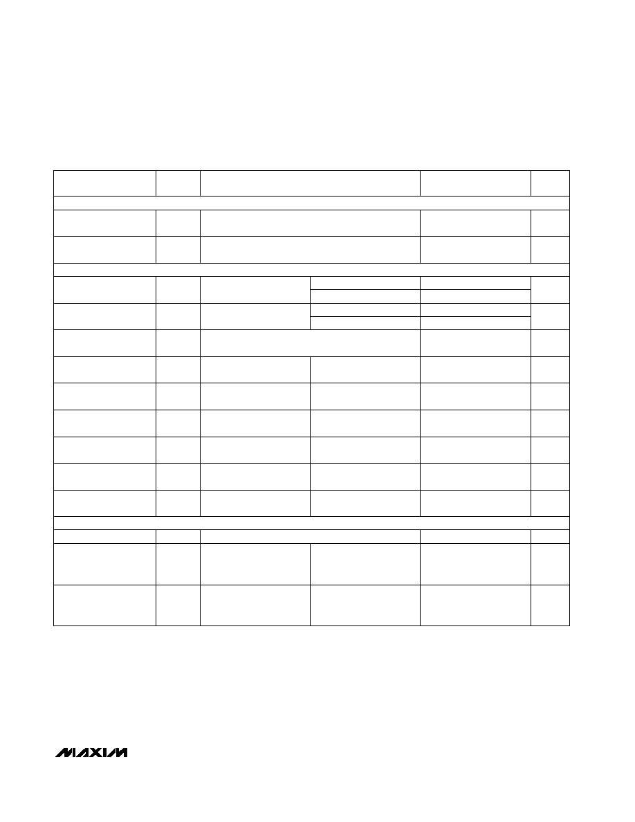
SWITCHES SHOWN FOR LOGIC "0" INPUT
DIP/SO/TSSOP
MAX392
LOGIC
SWITCH
0
1
OFF
ON
TOP VIEW
DIP/SO/TSSOP
MAX391
LOGIC
SWITCH
0
1
ON
OFF
DIP/SO/TSSOP
MAX393
LOGIC
SWITCHES
1, 4
0
1
OFF
ON
SWITCHES
2, 3
ON
OFF
16
15
14
13
12
11
10
9
1
2
3
4
5
6
7
8
IN2
COM2
NC2
V+
V-
NO1
COM1
IN1
MAX393
N.C.
NC3
COM3
IN3
IN4
COM4
NO4
GND
16
15
14
13
12
11
10
9
1
2
3
4
5
6
7
8
IN2
COM2
NC2
V+
V-
NC1
COM1
IN1
MAX391
N.C.
NC3
COM3
IN3
IN4
COM4
NC4
GND
16
15
14
13
12
11
10
9
1
2
3
4
5
6
7
8
IN2
COM2
NO2
V+
V-
NO1
COM1
IN1
MAX392
N.C.
NO3
COM3
IN3
IN4
COM4
NO4
GND
N.C. = NO CONNECT
_____________________Pin Configurations/Functional Diagrams/Truth Tables
For free samples & the latest literature: http://www.maxim-ic.com, or phone 1-800-998-8800.
For small orders, phone 1-800-835-8769.
19-0236; Rev 1; 6/99
Ordering Information continued at end of data sheet.
* Contact factory for dice specifications.
** Contact factory for availability and processing to MIL-STD-883.
16 TSSOP
-40∞C to +85∞C
MAX391EUE
16 Narrow SO
-40∞C to +85∞C
MAX391ESE
16 Plastic DIP
-40∞C to +85∞C
MAX391EPE
16 Narrow SO
0∞C to +70∞C
MAX391CSE
16 Plastic DIP
0∞C to +70∞C
MAX391CPE
PIN-PACKAGE
TEMP. RANGE
PART
16 TSSOP
0∞C to +70∞C
MAX391CUE
Dice*
0∞C to +70∞C
MAX391C/D

MAX391/MAX392/MAX393
Precision, Quad, SPST Analog Switches
2
_______________________________________________________________________________________
Voltage Referenced to V-
V+ .......................................................................-0.3V to +17V
GND....................................................................-0.3V to +17V
GND..........................................................-0.3V to (V+ + 0.3V)
V
IN
, V
COM
, V
NC
, V
NO
(Note 1) ........................................V- to V+
Current (any terminal) .........................................................30mA
Peak Current, COM, NO, NC
(pulsed at 1ms, 10% duty cycle max) ..........................100mA
ESD per Method 3015.7 ..................................................>2000V
Continuous Power Dissipation (T
A
= +70∞C)
Plastic DIP (derate 10.53mW/∞C above+70∞C) ...........842mW
Narrow SO (derate 8.70mW/∞C above +70∞C) ............696mW
TSSOP (derate 6.7mW/∞C above +70∞C) ....................457mW
CERDIP (derate 10.00mW/∞C above +70∞C) ...............800mW
Operating Temperature Ranges
MAX39_C_ _ .......................................................0∞C to +70∞C
MAX39_E_ _.....................................................-40∞C to +85∞C
MAX39_M_ _ ..................................................-55∞C to +125∞C
Storage Temperature Range .............................-65∞C to +150∞C
Lead Temperature (soldering, 10s) .................................+300∞C
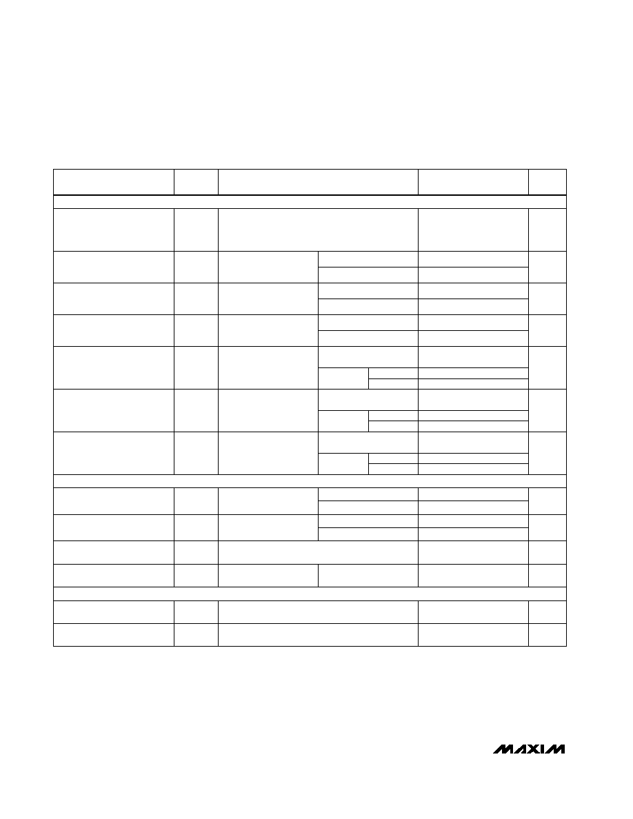
ELECTRICAL CHARACTERISTICS--Dual Supplies
(V+ = +5V ±10%, V- = -5V ±10%, GND = 0V, V
INH
= 2.4V, V
INL
= 0.8V, T
A
= T
MIN
to T
MAX
, unless otherwise noted.)
Stresses beyond those listed under "Absolute Maximum Ratings" may cause permanent damage to the device. These are stress ratings only, and functional
operation of the device at these or any other conditions beyond those indicated in the operational sections of the specifications is not implied. Exposure to
absolute maximum rating conditions for extended periods may affect device reliability.
Note 1:
Signals on NC, NO, COM, or IN exceeding V+ or V- are clamped by internal diodes. Limit forward diode current to maxi-
mum current rating.
ABSOLUTE MAXIMUM RATINGS
±
±
-5.0
5.0
-20
20
COM On Leakage Current
(Note 6)
nA
PARAMETER
SYMBOL
MIN
TYP
MAX
(Note 2)
UNITS
On-Resistance
R
ON
45
20
35
0.3
2
On-Resistance Match Between
Channels (Note 4)
R
ON
Analog Signal Range
V
COM
,
V
NO
,
V
NC
V-
V+
V
On-Resistance Flatness
(Note 5)
R
FLAT(ON)
1
4
-0.1
0.01
0.1
NO or NC Off Leakage Current
(Note 6)
I
NO(OFF)
or
I
NC(OFF)
nA
-2.5
2.5
COM Off Leakage Current
(Note 6)
-2.5
2.5
nA
I
COM(OFF)
I
COM(ON)
CONDITIONS
V+ = 5V, V- = -5V,
I
COM
= -10mA,
V
NO
or V
NC
= ±3V
V+ = 4.5V,
V- = -4.5V,
I
COM
= -10mA,
V
NO
or V
NC
= ±3.5V
V+ = 5V, V- = -5V,
I
COM
= -10mA,
V
NO
or V
NC
= ±3V
V+ = 5.5V,
V- = -5.5V,
V
COM
= ±4.5V,
V
NO
or V
NC
= 4.5V
(Note 3)
V+ = 5.5V,
V- = -5.5V,
V
COM
= ±4.5V,
V
NO
or V
NC
= 4.5V
V+ = 5.5V,
V- = -5.5V,
V
COM
= ±4.5V,
V
NO
or V
NC
= ±4.5V
T
A
= +25∞C
T
A
= +25∞C
T
A
= +25∞C
T
A
= T
MIN
to T
MAX
T
A
= +25∞C
T
A
= T
MIN
to T
MAX
T
A
= +25∞C
T
A
= T
MIN
to T
MAX
T
A
=
+25∞C
T
A
= T
MIN
to T
MAX
C, E
C, E
C, E
T
A
= T
MIN
to T
MAX
T
A
= T
MIN
to T
MAX
M
M
M
4
6
-0.1
0.01
0.1
-5
5
-5
5
-0.2
0.01
0.2
C, E
M
20
30
ANALOG SWITCH
MAX391/MAX392/MAX393
Precision, Quad, SPST Analog Switches
_______________________________________________________________________________________
3
ELECTRICAL CHARACTERISTICS--Dual Supplies (continued)
(V+ = +5V ±10%, V- = -5V ±10%, GND = 0V, V
INH
= 2.4V, V
INL
= 0.8V, T
A
= T
MIN
to T
MAX
, unless otherwise noted.)
PARAMETER
SYMBOL
MIN
TYP
MAX
(Note 2)
UNITS
Input Current with Input
Voltage High
I
INH
-0.5
0.005
0.5
µA
CONDITIONS
IN = 2.4V, all others = 0.8V
Input Current with Input
Voltage Low
I
INL
-0.5
0.005
0.5
µA
IN = 0.8V, all others = 2.4V
Turn-On Time
t
ON
65
130
ns
Charge Injection
(Note 3)
Q
2
5
pC
C
L
= 1.0nF, V
GEN
= 0V,
R
GEN
= 0
, Figure 4
T
A
= +25∞C
T
A
= T
MIN
to T
MAX
175
V
COM
= ±3V, Figure 2
T
A
= +25∞C
T
A
= T
MIN
to T
MAX
100
V
COM
= ±3V, Figure 2
Turn-Off Time
t
OFF
35
75
ns
MAX393 only, R
L
= 300
, C
L
= 35pF, Figure 3
Break-Before-Make
Time Delay (Note 3)
t
D
5
10
ns
T
A
= +25∞C
T
A
= +25∞C
R
L
= 50
, C
L
= 5pF,
f = 1MHz, Figure 5
Off Isolation (Note 7)
OIRR
72
dB
T
A
= +25∞C
R
L
= 50
, C
L
= 5pF,
f = 1MHz, Figure 6
Crosstalk (Note 8)
85
dB
T
A
= +25∞C
f = 1MHz, Figure 7
NC or NO Capacitance
C
(OFF)
9
pF
T
A
= +25∞C
f = 1MHz, Figure 7
COM Off Capacitance
C
COM(OFF)
9
pF
T
A
= +25∞C
f = 1MHz, Figure 8
COM On Capacitance
C
COM(ON)
pF
22
Power-Supply Range
-8.0
+8.0
V
Positive Supply Current
I+
V+ = 5.5V, V- = -5.5V,
V
IN
= 0V or V+,
All channels on or off
T
A
= T
MIN
to T
MAX
-1
1
µA
Negative Supply
Current
I-
V+ = 5.5V, V- = -5.5V,
V
IN
= 0V or V+,
All channels on or off
T
A
= T
MIN
to T
MAX
-1
1
µA
LOGIC INPUT
SUPPLY
DYNAMIC
MAX391/MAX392/MAX393
Precision, Quad, SPST Analog Switches
4
_______________________________________________________________________________________
ELECTRICAL CHARACTERISTICS--Single +5V Supply
(V+ = +5V ±10%, V- = 0V ±10%, GND = 0V, V
INH
= 2.4V, V
INL
= 0.8V, T
A
= T
MIN
to T
MAX
, unless otherwise noted.)
PARAMETER
SYMBOL
MIN
TYP
MAX
(Note 2)
UNITS
Analog Signal Range
V
COM,
V
NO,
V
NC
0
V+
V
CONDITIONS
(Note 3)
On-Resistance
R
ON
30
60
V+ = 4.5V,
I
COM
= -10mA,
V
NO
or V
NC
= 3.5V
Turn-On Time
t
ON
85
170
ns
V
NO
or V
NC
= 3V
Break-Before-Make Time
Delay (Note 3)
t
D
10
ns
MAX393 only, R
L
= 300
, C
L
= 35pF
Turn-Off Time
t
OFF
25
50
ns
V
NO
or V
NC
= 3V
Negative Supply Current
I-
-1
1
µA
Positive Supply Current
I+
-1
1
µA
Charge Injection
(Note 3)
Q
1
5
pC
C
L
= 1.0nF, V
GEN
= 0V,
R
GEN
= 0
, Figure 4
On-Resistance Match
Between Channels (Note 4)
R
ON
0.8
2
V+ = 5V,
I
COM
= -1.0mA,
V
NO
or V
NC
= 3V
On-Resistance Flatness
(Notes 3, 5)
R
FLAT(ON)
2
6
V+ = 5V,
I
COM
= -1.0mA,
V
NO
or V
NC
= 1V, 3V
NO or NC Off Leakage
Current (Note 9)
I
NO(OFF)
or
I
NC(OFF)
-0.25
0.01
0.25
nA
V+ = 5.5V,
V
COM
= 0V,
V
NO
or V
NC
= 4.5V
COM Off Leakage Current
(Note 9)
I
COM(OFF)
-0.1
0.1
nA
V+ = 5.5V,
V
COM
= 0V,
V
NO
or V
NC
= 4.5V
COM On Leakage Current
(Note 9)
I
COM(ON)
-0.2
0.2
nA
V+ = 5.5V,
V
COM
= 5V,
V
NO
or V
NC
= 4.5V
T
A
= +25∞C
T
A
= +25∞C
T
A
= +25∞C
T
A
= +25∞C
T
A
= +25∞C
T
A
= +25∞C
T
A
= T
MIN
to T
MAX
T
A
= T
MIN
to T
MAX
T
A
= T
MIN
to T
MAX
75
4
8
-0.1
0.1
-2.5
2.5
T
A
= T
MIN
to T
MAX
T
A
= T
MIN
to T
MAX
T
A
= T
MIN
to T
MAX
C, E
M
C, E
M
C, E
M
-5.0
5.0
-2.5
2.5
-20
20
-5.0
5.0
T
A
= +25∞C
T
A
= +25∞C
T
A
= T
MIN
to T
MAX
T
A
= T
MIN
to T
MAX
240
100
T
A
= +25∞C
V+ = 5.5V, V
IN
= 0V or V+, all channels on or off
V+ = 5.5V, V
IN
= 0V or V+, all channels on or off
ANALOG SWITCH
DYNAMIC
SUPPLY

MAX391/MAX392/MAX393
Precision, Quad, SPST Analog Switches
_______________________________________________________________________________________
5
ELECTRICAL CHARACTERISTICS--Single +3.3V Supply
(V+ = +3.0V to +3.6V, GND = 0V, V
INH
= 2.4V, V
INL
= 0.8V, T
A
= T
MIN
to T
MAX
, unless otherwise noted.)
Note 2:
The algebraic convention, where the most negative value is a minimum and the most positive value a maximum, is used in
this data sheet.
Note 3:
Guaranteed by design.
Note 4:
R
ON
=
R
ON
max -
R
ON
min.
Note 5:
Flatness is defined as the difference between the maximum and minimum value of on-resistance as measured over the
specified analog signal range.
Note 6:
Leakage parameters are 100% tested at maximum rated hot temperature and guaranteed by correlation at +25∞C.
Note 7:
Off Isolation = 20log
10
[ V
COM
/ (V
NC or
V
NO)
], V
COM
= output, V
NC or
V
NO
= input to off switch.
Note 8:
Between any two switches.
Note 9:
Leakage testing at single supply is guaranteed by testing with dual singles.
PARAMETER
SYMBOL
MIN
TYP
MAX
(Note 2)
UNITS
Analog Signal Range
V
COM,
V
NO,
V
NC
0
V+
V
CONDITIONS
(Note 3)
Channel On-Resistance
R
ON
83
175
V+ = 3V,
I
COM
= -1.0mA,
V
NO
or V
NC
= 1.5V
Turn-On Time (Note 3)
t
ON
160
400
ns
V
NO
or V
NC
= 1.5V
Break-Before-Make Time
Delay (Note 3)
t
D
20
ns
MAX393 only,
R
L
= 300
, C
L
= 35pF
Turn-Off Time (Note 3)
t
OFF
40
125
ns
V
NO
or V
NC
= 1.5V
Negative Supply Current
I-
-1
1
µA
Positive Supply Current
I+
-1
1
µA
Charge Injection (Note 3)
Q
1
5
pC
C
L
= 1.0nF,
V
GEN
= 0V, R
GEN
= 0V
V+ = 3.6V, V
IN
= 0V or V+, all channels on or off
V+ = 3.6V, V
IN
= 0V or V+, all channels on or off
T
A
= +25∞C
T
A
= +25∞C
T
A
= +25∞C
T
A
= +25∞C
T
A
= +25∞C
T
A
= T
MIN
to T
MAX
T
A
= T
MIN
to T
MAX
T
A
= T
MIN
to T
MAX
275
500
175
ANALOG SWITCH
DYNAMIC
SUPPLY