 | ÐлекÑÑоннÑй компоненÑ: MAX4163 | СкаÑаÑÑ:  PDF PDF  ZIP ZIP |
MAX4162/3/4 DS
General Description
The MAX4162/MAX4163/MAX4164 are single/dual/quad,
micropower operational amplifiers that combine an
exceptional bandwidth to power consumption ratio with
true rail-to-rail inputs and outputs. They consume a
mere 25µA quiescent current per amplifier, yet achieve
200kHz gain-bandwidth product and are unity-gain
stable while driving any capacitive load. The MAX4162/
MAX4163/MAX4164 operate from either a single supply
(2.7V to 10V) or dual supplies (±1.35V to ±5V), with an
input common-mode voltage range that extends 250mV
beyond either supply rail. These amplifiers use a propri-
etary architecture to achieve a very high input common-
mode rejection ratio without the midswing nonlinearities
present in other Rail-to-Rail
®
op amps. This architec-
ture also maintains high open-loop gain and output
swing while driving substantial loads.
The combination of excellent bandwidth/power perfor-
mance, single-supply operation, and miniature footprint
makes these op amps ideal for portable equipment and
other low-power, single-supply applications. The single
MAX4162 is available in 8-pin SO and space-saving
5-pin SOT23 packages. The MAX4163 is available in an 8-
pin ultra chip-scale package (UCSPTM) and an 8-pin µMAX
or SO package. The MAX4164 is available in a 14-pin SO
package.
________________________Applications
Battery-Powered Devices
Medical Instruments
pH Probes
Ionization Detectors
Portable Equipment
Cellular Phones
Low-Power, Low-Voltage
Equipment
Features
o UCSP Package (MAX4163)
o 1.0pA Typical Input Bias Current
o Single-Supply Operation from 2.7V to 10V
o Input Common-Mode Voltage Range Extends
250mV Beyond Either Supply Rail
o Rail-to-Rail Output Swing
o 200kHz Gain-Bandwidth Product
o 25µA Quiescent Current per Amplifier
o Excellent CMRR, PSRR, and Gain Linearity
o No Phase Reversal for Overdriven Inputs
o Unity-Gain Stable
o Stable with Any Capacitive Load
o Internally Short-Circuit Protected to Either Rail
MAX4162/MAX4163/MAX4164
UCSP, Micropower, Single-Supply, 10V,
Rail-to-Rail I/O Op Amps
________________________________________________________________ Maxim Integrated Products
1
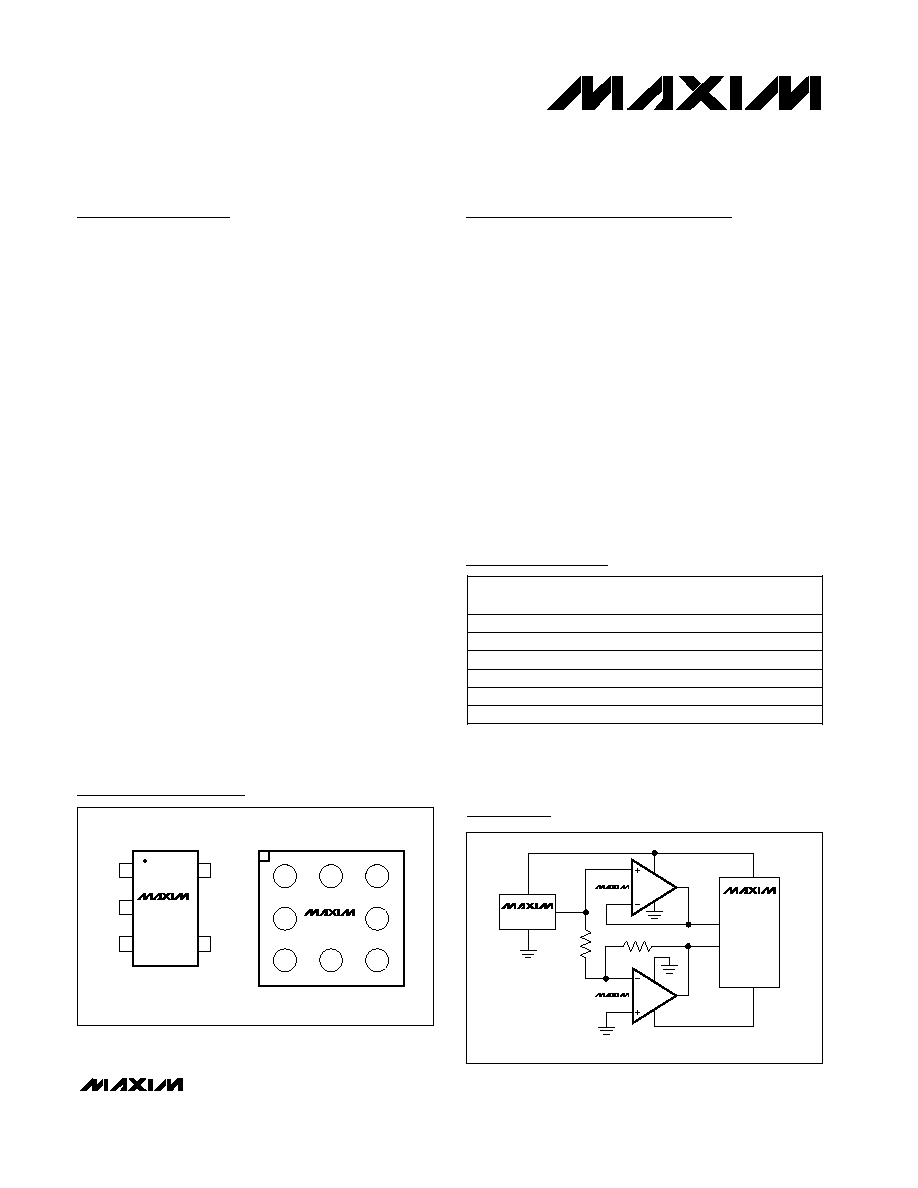
MAX152
1/2 MAX4163
1/2 MAX4163
MAX6120
MICROPOWER
±1.2V REFERENCE
V
REF+
V
DD
V
DD
V
DD
V
SS
V
SS
R
V
SS
-1.2V
+1.2V
V
OUT
V
OUT
GND
V
IN
3V
IN+
IN-
R
IN-
IN+
V
OUT
-3V
V
REF-
Typical Application Circuit
Pin Configurations
19-1195; Rev 1; 3/02
PART
MAX4162ESA
-40°C to +85°C
TEMP
RANGE
PIN-
PACKAGE
8 SO
Ordering Information
For pricing, delivery, and ordering information, please contact Maxim/Dallas Direct! at
1-888-629-4642, or visit Maxim's website at www.maxim-ic.com.
TOP
MARK
--
TOP VIEW
TOP VIEW (BUMPS SIDE DOWN)
V
SS
IN-
IN+
1
5
V
DD
OUT
MAX4162
MAX4163
SOT23
2
3
4
A
B
C
1
2
3
OUTA
V
DD
OUTB
INA-
INB-
INB+
V
SS
INA+
UCSP (B9-2)
MAX4162EUK-T
-40°C to +85°C
5 SOT23-5
AABX
MAX4163EBL-T* -40°C to +85°C
8 UCSP-8
AAX
MAX4163EUA
-40°C to +85°C
8 µMAX
--
Pin Configurations continued at end of data sheet.
*UCSP reliability is integrally linked to the user's assembly
methods, circuit board material, and environment. Refer to the
UCSP Reliability Notice in the UCSP Reliability section of this
data sheet for more information.
MAX4164ESD
-40°C to +85°C
14 SO
--
Rail-to-Rail is a registered trademark of Nippon Motorola Ltd.
UCSP is a trademark of Maxim Integrated Products, Inc.
MAX4163ESA
-40°C to +85°C
8 SO
--
MAX4162/MAX4163/MAX4164
UCSP, Micropower, Single-Supply, 10V,
Rail-to-Rail I/O Op Amps
2
_______________________________________________________________________________________
ABSOLUTE MAXIMUM RATINGS
ELECTRICAL CHARACTERISTICS: 3V Operation
(V
DD
= 3V, V
SS
= 0, V
CM
= V
DD
/2, V
OUT
= V
DD
/2, R
L
tied to V
DD
/2, T
A
= -40°C to +85°C, unless otherwise noted. Typical values are
at T
A
= +25°C.) (Note 1)
Stresses beyond those listed under "Absolute Maximum Ratings" may cause permanent damage to the device. These are stress ratings only, and functional
operation of the device at these or any other conditions beyond those indicated in the operational sections of the specifications is not implied. Exposure to
absolute maximum rating conditions for extended periods may affect device reliability.
Supply Voltage (V
DD
to V
SS
) ..................................................11V
IN+, IN-, OUT Voltage ......................(V
DD
+ 0.3V) to (V
SS
- 0.3V)
Short-Circuit Duration (to either rail)...........................Continuous
Continuous Power Dissipation (T
A
= +70°C)
5-Pin SOT23 (derate 7.1mW/°C above +70°C)..............571mW
8-Pin SO (derate 5.88mW/°C above +70°C)..................471mW
8-Pin UCSP (derate 4.7mW/°C above +70°C) ...............379mW
8-Pin µMAX (derate 4.1mW/°C above +70°C) ...............330mW
14-Pin SO (derate 8.00mW/°C above +70°C)................640mW
Operating Temperature Range ...........................-40°C to +85°C
Storage Temperature Range .............................-65°C to +150°C
Junction Temperature ......................................................+150°C
Lead Temperature (soldering, 10s) .................................+300°C
To either supply rail
V
OL
- V
SS
V
DD
- V
OH
V
OL
- V
SS
V
DD
- V
OH
Inferred from PSRR test
R
L
= 10k
Inferred from CMRR test
T
A
= +25°C
T
A
= -40°C to +85°C
T
A
= +25°C
T
A
= -40°C to +85°C
CONDITIONS
15
I
SC
mV
3
25
R
L
= 100k
V
OUT
3
25
30
180
R
L
= 10k
30
180
dB
A
V
85
120
dB
CMRR
70
100
pA
1.0
100
V
2.7
10.0
V
DD
I
B
T
V
SS
- V
DD
+
0.25
0.25
V
CM
>10
R
IN
±6
±0.5
±5
MAX4164
±0.5
±3
V
OS
±4
MAX4162
±0.5
±4
mV
±5
MAX4163
UNITS
MIN
TYP
MAX
SYMBOL
A
V
= 1V/V
kHz
200
GBWP
V
DD
= 2.7V to 10V
PSRR
dB
80
110
mA
0.1
R
OUT
V
V
CM
= (V
SS
- 0.25V) to (V
DD
+ 0.25V)
µV/°C
TCV
OS
2
T
A
= +25°C
T
A
= -40°C to +85°C
µA
25
40
I
DD
degrees
60
M
dB
12
GM
V
OUT
= 1V to 2V step
µs
50
V
DD
= 0 to 3V step, V
IN
= V
DD
/2, A
V
= 1V/V
µs
20
t
ON
V/ms
115
SR
f = 1kHz, V
OUT
= 2V
P-P
, R
L
= 100k
, A
V
= 1V/V
THD
%
0.02
Phase Margin
Gain Margin
Output Short-Circuit Current
Output Voltage Swing
Input Offset Voltage Tempco
Settling Time to 0.1%
Large-Signal Voltage Gain
Supply Current (Per Amplifier)
Turn-On Time
Slew Rate
Total Harmonic Distortion
Common-Mode Rejection Ratio
Operating Voltage Range
Input Bias Current (Note 2)
Input Common-Mode Voltage
Range
Differential Input Resistance
Input Offset Voltage
PARAMETER
Gain-Bandwidth Product
Power-Supply Rejection Ratio
Closed-Loop Output Resistance
MAX4162/MAX4163/MAX4164
UCSP, Micropower, Single-Supply, 10V,
Rail-to-Rail I/O Op Amps
_______________________________________________________________________________________
3
ELECTRICAL CHARACTERISTICS: 3V Operation (continued)
(V
DD
= 3V, V
SS
= 0, V
CM
= V
DD
/2, V
OUT
= V
DD
/2, R
L
tied to V
DD
/2, T
A
= -40°C to +85°C, unless otherwise noted. Typical values are
at T
A
= +25°C.) (Note 1)
ELECTRICAL CHARACTERISTICS: 5V Operation
(V
DD
= 5V, V
SS
= 0, V
CM
= V
DD
/2, V
OUT
= V
DD
/2, R
L
tied to V
DD
/2, T
A
= -40°C to +85°C, unless otherwise noted. Typical
values are at T
A
= +25°C.) (Note 1)
pF
CONDITIONS
nV/
Hz
e
n
80
f = 1kHz
Input Voltage-Noise Density
Input Common-Mode
Capacitance
pF
1.5
Differential Input Capacitance
0.7
PARAMETER
UNITS
MIN
TYP
MAX
SYMBOL
kHz
Internal Charge-Pump
Frequency
700
µV
P-P
Charge-Pump Output
Feedthrough
100
To either supply rail
V
OL
- V
SS
V
DD
- V
OH
V
V
OL
- V
SS
V
DD
- V
OH
V
CM
= (V
SS
- 0.25V) to (V
DD
+ 0.25V)
Inferred from PSRR test
degrees
60
R
L
= 10k
Inferred from CMRR test
M
dB
T
A
= +25°C
T
A
= -40°C to +85°C
T
A
= +25°C
12
T
A
= -40°C to +85°C
GM
CONDITIONS
15
I
SC
mV
5
40
R
L
= 100k
V
OUT
µV/°C
5
40
µA
50
300
R
L
= 10k
2
50
300
T
A
= +25°C
T
A
= -40°C to +85°C
dB
A
V
25
45
I
DD
85
120
dB
CMRR
Phase Margin
Gain Margin
Output Short-Circuit Current
Output Voltage Swing
70
100
Input Offset Voltage Tempco
Large-Signal Voltage Gain
Supply Current (Per Amplifier)
Common-Mode Rejection Ratio
Operating Voltage Range
pA
1.0
100
Input Bias Current (Note 2)
V
2.7
10.0
Input Common-Mode Voltage
Range
V
DD
I
B
T
V
SS
- V
DD
+
0.25
0.25
Differential Input Resistance
V
CM
Input Offset Voltage
>10
PARAMETER
Gain-Bandwidth Product
±6
Power-Supply Rejection Ratio
Closed-Loop Output Resistance
±0.5
±5
MAX4164
±0.5
±3
V
OS
±4
MAX4162
±0.5
±4
mV
±5
MAX4163
UNITS
MIN
TYP
MAX
SYMBOL
A
V
= 1V/V
kHz
200
GBWP
V
DD
= 2.7V to 10V
PSRR
dB
80
110
mA
0.1
R
OUT
MAX4162/MAX4163/MAX4164
UCSP, Micropower, Single-Supply, 10V,
Rail-to-Rail I/O Op Amps
4
_______________________________________________________________________________________
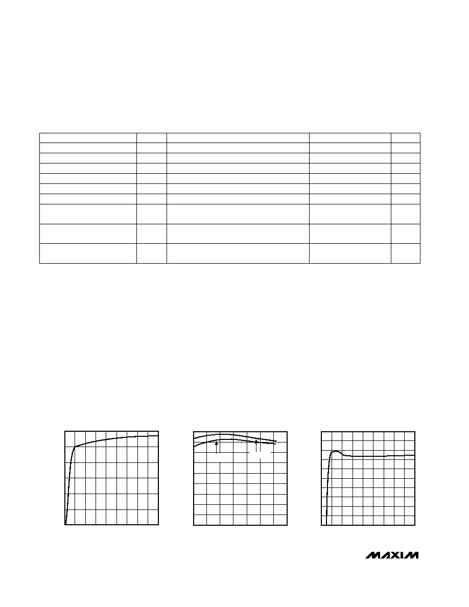
0
5
10
15
20
25
30
1
2
3
4
5
6
7
8
9
10
SUPPLY CURRENT
vs. SUPPLY VOLTAGE
MAX4162-01
SUPPLY VOLTAGE (V)
SUPPLY CURRENT (
µ
A)
10
12
14
16
18
20
22
24
26
28
-40
-20
0
20
40
60
80
100
SUPPLY CURRENT
vs. TEMPERATURE
MAX4162-02
TEMPERATURE (
°C)
SUPPLY CURRENT (
µ
A)
V
CC
= 5V
V
CC
= 3V
-150
-130
-110
-90
-70
-50
-30
-10
10
30
50
1
2
3
4
5
6
7
8
9
10
INPUT OFFSET VOLTAGE VARIATION
vs. SUPPLY VOLTAGE
MAX4162-03
SUPPLY VOLTAGE (V)
V
OS
(
µ
V)
ELECTRICAL CHARACTERISTICS: 5V Operation (continued)
(V
DD
= 5V, V
SS
= 0, V
CM
= V
DD
/2, V
OUT
= V
DD
/2, R
L
tied to V
DD
/2, T
A
= -40°C to +85°C, unless otherwise noted. Typical
values are at T
A
= +25°C.) (Note 1)
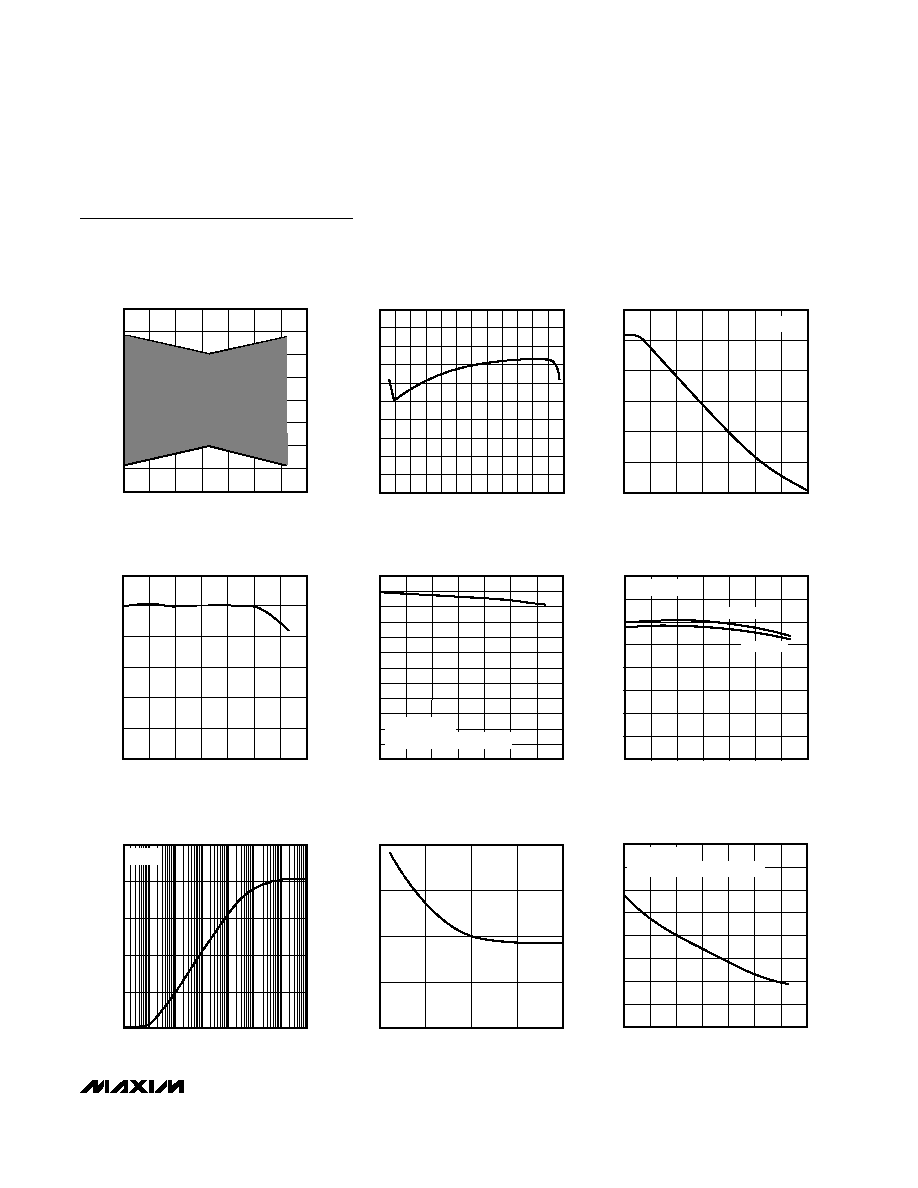
__________________________________________Typical Operating Characteristics
(V
DD
= 5V, V
SS
= 0, V
CM
= V
DD
/2, T
A
= +25°C, unless otherwise noted.)
Note 1: All device specifications are 100% tested at T
A
= +25°C. Limits over the extended temperature range are guaranteed by
design, not production tested.
Note 2: Input bias current guaranteed by design, not production tested.
pF
CONDITIONS
%
THD
0.02
f = 1kHz, V
OUT
= 2V
P-P
, R
L
= 100k
, A
V
= 1V/V
Total Harmonic Distortion
Input Common-Mode
Capacitance
V/ms
1.5
Slew Rate
115
PARAMETER
SR
kHz
Internal Charge-Pump
Frequency
700
µV
P-P
Charge-Pump Output
Feedthrough
100
UNITS
MIN
TYP
MAX
SYMBOL
V
OUT
= 1V to 2V step
µs
Settling Time to 0.1%
70
V
DD
= 0 to 3V step, V
IN
= V
DD
/2, A
V
= 1V/V
µs
Turn-On Time
40
t
ON
f = 1kHz
nV/
Hz
Input Voltage-Noise Density
80
e
n
pF
Differential Input Capacitance
0.7
MAX4162/MAX4163/MAX4164
UCSP, Micropower, Single-Supply, 10V,
Rail-to-Rail I/O Op Amps
_______________________________________________________________________________________
5
-1000
-750
-500
-250
0
250
500
750
1000
-40
-20
0
20
40
60
80
100
INPUT OFFSET VOLTAGE
vs. TEMPERATURE
MAX4162-04
TEMPERATURE (°C)
V
OS
(
µ
V)
-14
-12
-10
-8
-6
-4
-2
0
2
4
6
-0.5
0.5
1.5
2.5
3.5
4.5
5.5
INPUT OFFSET VOLTAGE VARIATION
vs. COMMON-MODE VOLTAGE
MAX4162-05
COMMON-MODE VOLTAGE (V)
V
OS
(
µ
V)
10
30
50
70
90
110
130
0.1
1
10
100
1k
10k 100k 1M
POWER-SUPPLY REJECTION RATIO
vs. FREQUENCY
MAX4162-08
FREQUENCY (Hz)
PSRR (dB)
A
V
= 1
0
10
20
30
40
50
70
60
80
100
90
110
120
COMMON-MODE REJECTION
vs. TEMPERATURE
MAX4162-10
TEMPERATURE (°C)
COMMON-MODE REJECTION (dB)
-40
-20
0
20
40
60
80
100
V
DD
= 3V OR 5V
V
CM
= -0.25V TO V
DD
+ 0.25V
10
30
50
70
90
110
130
-40
-20
0
20
40
60
80
100
POWER-SUPPLY REJECTION RATIO
vs. TEMPERATURE
MAX4162-09
TEMPERATURE (°C)
PSRR (dB)
0
20
40
60
80
100
120
140
160
OPEN-LOOP GAIN
vs. TEMPERATURE
MAX4162-11
TEMPERATURE (°C)
OPEN-LOOP GAIN (dB)
-40
-20
0
20
40
60
80
100
V
DD
= 3V OR 5V
R
L
= 10k
R
L
= 100k
0.1
1
10
100
1000
10,000
0.1
1
10
100
1k
10k
100k 1M
OUTPUT IMPEDANCE
vs. FREQUENCY
MAX4162-12a
FREQUENCY (Hz)
OUTPUT IMPEDANCE (
)
A
V
= 1
Typical Operating Characteristics (continued)
(V
DD
= 5V, V
SS
= 0, V
CM
= V
DD
/2, T
A
= +25°C, unless otherwise noted.)
0
5
10
15
20
25
30
35
40
SHORT-CIRCUIT OUTPUT CURRENT
vs. TEMPERATURE
MAX4162-13
TEMPERATURE (°C)
SHORT-CIRCUIT OUTPUT CURRENT (mA)
-40
-20
0
20
40
60
80
100
V
DD
= 3V OR 5V
SHORT TO EITHER SUPPLY RAIL
1.00
1.25
1.50
1.75
2.00
0
2.50
3.75
1.25
5.00
COMMON-MODE INPUT CAPACITANCE
vs. COMMON-MODE VOLTAGE
MAX4162-12b
COMMON-MODE VOLTAGE (V)
COMMON-MODE INPUT CAPACITANCE (pF)