 | –≠–ª–µ–∫—Ç—Ä–æ–Ω–Ω—ã–π –∫–æ–º–ø–æ–Ω–µ–Ω—Ç: MAX4250 | –°–∫–∞—á–∞—Ç—å:  PDF PDF  ZIP ZIP |
For free samples & the latest literature: http://www.maxim-ic.com, or phone 1-800-998-8800.
For small orders, phone 408-737-7600 ext. 3468.
General Description
The MAX4249≠MAX4257 low-noise, low-distortion oper-
ational amplifiers offer Rail-to-Rail
Æ
outputs and single-
supply operation down to 2.4V. They draw only 400µA
of quiescent supply current per amplifier while featuring
ultra-low distortion (0.0002% THD), as well as low input
voltage noise density (7.9nV/
Hz) and low input current
noise density (0.5fA/
Hz). These features make the
devices an ideal choice for portable/battery-powered
applications that require low distortion and/or low noise.
For additional power conservation, the MAX4249/
MAX4251/MAX4253/MAX4256 offer a low-power shut-
down mode that reduces supply current to 0.5µA and
puts the amplifiers' outputs into a high-impedance state.
The MAX4249≠MAX4257's outputs swing rail-to-rail and
their input common-mode voltage range includes
ground. The MAX4250≠MAX4254 are unity-gain stable;
the MAX4249/MAX4255/MAX4256/MAX4257 are internal-
ly compensated for gains of 10V/V or greater. The single
MAX4250/MAX4255 are available in a space-saving,
5-pin SOT23 package.
Applications
Portable/Battery-Powered Equipment
Medical Instrumentation
ADC Buffers
Digital Scales
Strain Gauges
Sensor Amplifiers
Portable Communications Devices
____________________________Features
o
Low Input Voltage Noise Density: 7.9nV/
Hz
o
Low Input Current Noise Density: 0.5fA/
Hz
o
Low Distortion: 0.0002% THD (1k
load)
o
400µA Quiescent Supply Current per Amplifier
o
Single-Supply Operation from +2.4V to +5.5V
o
Input Common-Mode Voltage Range Includes
Ground
o
Outputs Swing within 8mV of Rails with a 10k
Load
o
3MHz GBW Product, Unity-Gain Stable
(MAX4250≠MAX4254)
22MHz GBW Product, Stable with A
V
10V/V
(MAX4249/MAX4255/MAX4256/MAX4257)
o
Excellent DC Characteristics:
V
OS
= 70µV
I
BIAS
= 1pA
Large-Signal Voltage Gain = 116dB
o
Low-Power Shutdown Mode:
Reduces Supply Current to 0.5µA
Places Outputs in a High-Impedance State
o
400pF Capacitive-Load Handling Capability
o
Available in Space-Saving SOT23 and µMAX
Packages
MAX4249≠MAX4257
SOT23, Single-Supply, Low-Noise,
Low-Distortion, Rail-to-Rail Op Amps
________________________________________________________________
Maxim Integrated Products
1
19-1295; Rev 2; 4/98
PART
MAX4249
ESD
MAX4249EUB
-40∞C to +85∞C
-40∞C to +85∞C
TEMP. RANGE
PIN-
PACKAGE
14 SO
10 µMAX
Ordering Information
Selector Guide
Ordering Information continued at end of data sheet.
Pin Configurations and Typical Operating Circuit appear at
end of data sheet.
Rail-to-Rail is a registered trademark of Nippon Motorola Ltd.
GAIN
BANDWIDTH
(MHz)
MAX4249
22
PART
MINIMUM
STABLE
GAIN (V/V)
10
SHUTDOWN
MODE
PACKAGES
2
Yes
10-pin µMAX, 14-pin SO
NO. OF AMPLIFIERS
PER PACKAGE
MAX4250
3
1
1
--
5-pin SOT23
MAX4251
3
1
1
Yes
8-pin µMAX/SO
MAX4252
3
1
2
--
8-pin µMAX/SO
MAX4253
3
1
2
Yes
10-pin µMAX, 14-pin SO
MAX4254
3
1
4
--
14-pin SO
MAX4255
22
10
1
--
5-pin SOT23
MAX4256
22
10
1
Yes
8-pin µMAX/SO
MAX4257
22
10
2
--
8-pin µMAX/SO
SOT
TOP MARK
--
--
MAX4250
EUK-T -40∞C to +85∞C
5 SOT23-5
ACCI
MAX4249≠MAX4257
SOT23, Single-Supply, Low-Noise,
Low-Distortion, Rail-to-Rail Op Amps
2
_______________________________________________________________________________________
ABSOLUTE MAXIMUM RATINGS
ELECTRICAL CHARACTERISTICS
(V
DD
= +5V, V
SS
= 0V, V
CM
= 0V, V
OUT
= V
DD
/2, R
L
tied to V
DD
/2, SHDN = V
DD
or open, T
A
= -40∞C to +85∞C, unless otherwise
noted. Typical values are at T
A
= +25∞C.) (Notes 1, 2)
Stresses beyond those listed under "Absolute Maximum Ratings" may cause permanent damage to the device. These are stress ratings only, and functional
operation of the device at these or any other conditions beyond those indicated in the operational sections of the specifications is not implied. Exposure to
absolute maximum rating conditions for extended periods may affect device reliability.
Power-Supply Voltage (V
DD
to V
SS
) ......................+6.0V to -0.3V
Analog Input Voltage (IN_+, IN_-)....(V
DD
+ 0.3V) to (V
SS
- 0.3V)
SHDN Input Voltage....................................+6.0V to (V
SS
- 0.3V)
Output Short-Circuit Duration to Either Supply ..........Continuous
Continuous Power Dissipation (T
A
= +70∞C)
5-Pin SOT23 (derate 7.1mW/∞C above +70∞C)............571mW
8-Pin µMAX (derate 4.10mW/∞C above +70∞C) ...........330mW
8-Pin SO (derate 5.88mW/∞C above +70∞C)................471mW
10-Pin µMAX (derate 5.6mW/∞C above +70∞C) ...........444mW
14-Pin SO (derate 8.33mW/∞C above +70∞C)..............667mW
Operating Temperature Range ...........................-40∞C to +85∞C
Junction Temperature ......................................................+150∞C
Storage Temperature Range .............................-65∞C to +160∞C
Lead Temperature (soldering, 10sec) .............................+300∞C
Normal mode
SHDN = V
SS
to V
DD
(Note 3)
Shutdown mode (SHDN = V
SS
),
V
OUT
= V
SS
to V
DD
V
IN+
- V
IN-
10mV,
R
L
= 10k
to V
DD
/2
V
SS
- 0.2V
V
CM
V
DD
- 1.1V
Guaranteed by CMRR test
R
L
= 1k
to V
DD
/2, V
OUT
= 150mV to 4.75V
(Note 4)
Shutdown mode (SHDN = V
SS
) (Note 1)
R
L
= 10k
to V
DD
/2, V
OUT
= 25mV to 4.97V
(Note 4)
V
DD
= 2.4V to 5.5V
CONDITIONS
pF
11
Input Capacitance
µA
0.5
1.5
I
IL
/I
IH
SHDN Input Current
V
0.8 x V
DD
V
IH
SHDN Logic High
V
0.2 x V
DD
V
IL
SHDN Logic Low
µA
0.001
1.0
I
LEAK
Output Leakage Current
mA
68
I
SC
Output Short-Circuit Current
7
20
V
IN+
- V
IN-
10mV,
R
L
= 1k
to V
DD
/2
8
25
dB
80
112
A
V
80
116
Large-Signal Voltage Gain
dB
75
100
PSRR
Power-Supply Rejection Ratio
420
575
400
V
2.4
5.5
V
DD
Supply-Voltage Range
Quiescent Supply Current
per Amplifier
dB
70
115
CMRR
Common-Mode Rejection
Ratio
V
-0.2
V
DD
-
1.1
V
CM
Input Common-Mode Voltage
Range
G
1000
R
IN
Differential Input Resistance
pA
±1
±100
I
OS
Input Offset Current
µA
0.5
1.5
I
Q
±0.07
±0.75
V
OS
mV
Input Offset Voltage
pA
±1
±100
I
B
Input Bias Current
UNITS
MIN
TYP
MAX
SYMBOL
PARAMETER
0.3
µV/∞C
Input Offset Voltage Tempco
mV
47
100
V
OUT
77
200
Output Voltage Swing
V
DD
= 3V
V
DD
= 5V
V
DD
- V
OH
V
OL
- V
SS
V
DD
- V
OH
V
OL
- V
SS

MAX4249≠MAX4257
SOT23, Single-Supply, Low-Noise,
Low-Distortion, Rail-to-Rail Op Amps
_______________________________________________________________________________________
3
ELECTRICAL CHARACTERISTICS (continued)
(V
DD
= +5V, V
SS
= 0V, V
CM
= 0V, V
OUT
= V
DD
/2, R
L
tied to V
DD
/2, SHDN = V
DD
or open, T
A
= -40∞C to +85∞C, unless otherwise
noted. Typical values are at T
A
= +25∞C.) (Notes 1, 2)
Note 1:
SHDN is available on the MAX4249/MAX4251/MAX4253/MAX4256 only.
Note 2:
The MAX4249EUB, MAX425_EU_ specifications are 100% tested at T
A
= +25∞C. Limits over the extended temperature
range are guaranteed by design, not production tested.
Note 3:
Guaranteed by the Power-Supply Rejection Ratio (PSRR) test.
Note 4:
Guaranteed by design.
Note 5:
Lowpass filter bandwidth is 22kHz for f = 1kHz, and 80kHz for f = 20kHz. Noise floor of test equipment = 10nV/
Hz.
No sustained oscillations
f = 1kHz
MAX4250≠MAX4254
f = 30kHz
f = 1kHz
f = 0.1Hz to 10Hz
MAX4249/MAX4255/MAX4256/MAX4257
f = 10Hz
CONDITIONS
pF
400
0.006
0.0004
fA/
Hz
0.5
i
n
Input Current Noise Density
nV/
Hz
7.9
e
n
8.9
27
Input Voltage Noise Density
3
Gain-Bandwidth Product
nVp-p
760
e
n
(p-p)
Peak-to-Peak Input Noise
Voltage
MHz
22
GBW
UNITS
MIN
TYP
MAX
SYMBOL
PARAMETER
MAX4250≠MAX4254
MAX4249/MAX4255/MAX4256/MAX4257
0.3
Slew Rate
V/µs
2.1
SR
MAX4250≠MAX4254, A
V
= +1V/V
MAX4249/MAX4255/MAX4256/MAX4257,
A
V
= +10V/V
MAX4250≠MAX4254, A
V
= +1V/V
74
dB
12.5
G
M
Gain Margin
10
MAX4249/MAX4255/MAX4256/MAX4257,
A
V
= +10V/V
µs
1.6
Settling Time
6.7
degrees
68
M
Phase Margin
V
DD
= 0V to 5V step, V
OUT
stable to 0.1%
µs
6
t
PU
Power-Up Delay Time
MAX4250≠MAX4254, A
V
= +1V/V,
V
OUT
= 2Vp-p, R
L
= 1k
to GND
(Note 5)
f = 1kHz
f = 20kHz
Capacitive-Load Stability
0.0012
Total Harmonic
Distortion plus Noise
MAX4249/MAX4255/MAX4256/
MAX4257, A
V
= +10V/V,
R
F
= 100k
, R
G
= 11k
,
V
OUT
= 4Vp-p, R
L
= 10k
to GND
(Note 5)
%
THD+N
MAX4250≠MAX4254
MAX4249/MAX4255/MAX4256/
MAX4257
To 0.01%,
V
OUT
= 2V step
MAX4251/MAX4253
I
VDD
= 5% of
normal operation
µs
t
SH
Shutdown Delay Time
0.8
V
OUT
= 2.5V,
V
OUT
settles to
0.1%
µs
8
t
EN
Enable Delay Time
f = 20kHz
0.007
f = 1kHz
MAX4251/MAX4253
3.5
MAX4249/MAX4256
1.2
MAX4249/MAX4256

MAX4249≠MAX4257
SOT23, Single-Supply, Low-Noise,
Low-Distortion, Rail-to-Rail Op Amps
4
_______________________________________________________________________________________
Typical Operating Characteristics
(V
DD
= +5V, V
SS
= 0V, V
CM
= V
OUT
= V
DD
/2, input noise floor of test equipment = 10nV/
Hz for all distortion measurements,
T
A
= +25∞C, unless otherwise noted.)
0
10
5
20
15
25
30
35
40
-95
-55
-35
-75
-13
7
28
49
69
90
110
131
152
172
192
MAX4251/MAX4256 INPUT OFFSET
VOLTAGE DISTRIBUTION
MAX4249 TOC01
V
OS
(
µ
V)
NUMBER OF UNITS
400 UNITS
V
CM
= 0V
T
A
= +25∞C
-250
-100
-150
-200
-50
0
50
100
150
200
250
-40
0
-20
20
40
60
80
OFFSET VOLTAGE
vs. TEMPERATURE
MAX4249 TOC02
TEMPERATURE (∞C)
V
OS
(
µ
V)
V
CM
= 0V
-50
0
100
50
150
200
-0.5
1.5
0.5
2.5
3.5
4.5
INPUT OFFSET VOLTAGE vs.
COMMON-MODE INPUT VOLTAGE
MAX4249 TOC03
INPUT COMMON-MODE VOLTAGE (V)
INPUT OFFSET VOLTAGE (
µ
V)
V
DD
= 3V
V
DD
= 5V
0
0.3
0.2
0.1
0.4
0.5
0.6
0
4
3
1
2
5
6
7
8
9
10
OUTPUT VOLTAGE
vs. OUTPUT LOAD CURRENT
MAX4249 TOC04
OUTPUT LOAD CURRENT (mA)
OUTPUT VOLTAGE (V)
V
DD
= 3V OR 5V
V
DIFF
= ±10mV
V
OL
V
DD
- V
OH
50
70
60
100
90
80
130
120
110
140
0
100
50
150
200
250
LARGE-SIGNAL VOLTAGE GAIN
vs. OUTPUT VOLTAGE SWING
MAX4249TOC07
V
OUT
SWING FROM EITHER SUPPLY (mV)
A
V
(dB)
V
DD
= 3V
R
L
REFERENCED TO GND
R
L
= 200k
R
L
= 20k
R
L
= 2k
0
0.03
0.02
0.01
0.04
0.05
0.06
0.07
0.08
0.09
0.10
-40
0
-20
20
60
40
80
OUTPUT VOLTAGE SWING (V
OH
)
vs. TEMPERATURE
MAX4249 TOC05
TEMPERATURE (∞C)
V
DD -
V
OH
(V)
R
L
= 1k
R
L
= 10k
R
L
= 100k
0
0.02
0.01
0.03
0.04
0.05
0.06
-40
0
-20
20
60
40
80
OUTPUT VOLTAGE SWING (V
OL
)
vs. TEMPERATURE
MAX4249 TOC06
TEMPERATURE (∞C)
V
OL
(V)
R
L
= 1k
R
L
= 10k
R
L
= 100k
60
70
80
90
100
110
120
130
140
0
50
100
150
200
250
LARGE-SIGNAL VOLTAGE GAIN
vs. OUTPUT VOLTAGE SWING
MAX4249 TOC08
V
OUT
SWING FROM EITHER SUPPLY (mV)
A
V
(dB)
R
L
= 200k
R
L
= 2k
V
DD
= 3V
R
L
REFERENCED TO V
DD
R
L
= 20k
50
70
60
100
90
80
130
120
110
140
0
100
50
150
200
250
LARGE-SIGNAL VOLTAGE GAIN
vs. OUTPUT VOLTAGE SWING
MAX4249TOC09
V
OUT
SWING FROM EITHER SUPPLY (mV)
A
V
(dB)
V
DD
= 5V
R
L
REFERENCED TO GND
R
L
= 2k
R
L
= 20k
R
L
= 200k
MAX4249≠MAX4257
SOT23, Single-Supply, Low-Noise,
Low-Distortion, Rail-to-Rail Op Amps
_______________________________________________________________________________________
5
50
80
70
60
90
100
110
120
130
140
150
0
100
50
150
200
250
LARGE-SIGNAL VOLTAGE GAIN
vs. OUTPUT VOLTAGE SWING
MAX4249 TOC10
V
OUT
SWING FROM EITHER SUPPLY (mV)
A
V
(dB)
R
L
= 200k
R
L
= 20k
R
L
= 2k
V
DD
= 5V
R
L
REFERENCED TO V
DD
100
110
105
115
120
125
-40
0
-20
20
60
40
80
LARGE-SIGNAL VOLTAGE GAIN
vs. TEMPERATURE
MAX4249 TOC11
TEMPERATURE (∞C)
A
V
(dB)
R
L
REFERENCED T0 V
DD
/2
V
DD
= 5V
R
L
= 100k
V
OUT
= 10mV
to 4.99V
R
L
= 10k
V
OUT
= 20mV
to 4.975V
R
L
= 1k
V
OUT
= 150mV
to 4.75V
0.373
0.374
0.375
0.376
340
380
360
400
420
440
460
-40
0
-20
20
60
40
80
SUPPLY CURRENT AND SHUTDOWN
SUPPLY CURRENT vs. TEMPERATURE
MAX4249 TOC12
TEMPERATURE (∞C)
SHUTDOWN SUPPLY CURRENT (
µ
A)
SUPPLY CURRENT (
µ
A)
SHDN = V
DD
PER AMPLIFIER
SHDN = V
SS
320
340
360
380
400
420
440
0
0.1
0.2
0.3
0.4
0.5
0.6
1.8
2.8
2.3
3.3
3.8
4.3
4.8
5.3 5.5
SUPPLY CURRENT AND SHUTDOWN
SUPPLY CURRENT vs. SUPPLY VOLTAGE
MAX4249 TOC 13A
SUPPLY VOLTAGE (V)
SUPPLY CURRENT (µA)
SHUTDOWN SUPPLY CURRENT (
µ
A)
PER AMPLIFIER
SHDN = V
SS
SHDN = V
DD
60
-40
100
10k
100k
1M
1k
10M
MAX4250≠MAX4254
GAIN AND PHASE vs. FREQUENCY
-20
-10
0
-30
MAX4249 TOC15
FREQUENCY (Hz)
GAIN (dB)
PHASE (DEGREES)
10
20
30
40
50
180
-180
-108
-72
-36
-144
0
36
72
108
144
GAIN
PHASE
V
DD
= 3V, 5V
R
L
= 50k
C
L
= 20pF
A
V
= 1000
2000
100
0.001
0.1
1
0.01
5
SUPPLY CURRENT
vs. OUTPUT VOLTAGE
MAX4249 TOC13B
OUTPUT VOLTAGE (V)
SUPPLY CURRENT (
µ
A) 1000
400
V
DD
= 5V
V
DD
= 3V
40
60
80
120
100
180
160
140
1.8
2.3
2.8
3.3
3.8
4.3
4.8
5.3
INPUT OFFSET VOLTAGE
vs. SUPPLY VOLTAGE
MAX4249 TOC14
SUPPLY VOLTAGE (V)
V
OS
(
µ
V)
V
CM
= 0V
V
OUT
= V
DD
/2
R
L
REFERENCED TO GND
R
L
= 1k
R
L
= 10k
R
L
= 100k
60
-40
100
10k
100k
1M
1k
10M
MAX4249, MAX4255/MAX4256/MAX4257
GAIN AND PHASE vs. FREQUENCY
-20
-10
0
-30
MAX4249 TOC16
FREQUENCY (Hz)
GAIN (dB)
PHASE (DEGREES)
10
20
30
40
50
180
-180
-108
-72
-36
-144
0
36
72
108
144
V
DD
= 3V, 5V
R
L
= 50k
C
L
= 20pF
A
V
= 1000
GAIN
PHASE
0
-100
-110
1
1k
10k
100k
1M
10
100
10M
MAX4250≠MAX4254
POWER-SUPPLY REJECTION RATIO
vs. FREQUENCY
-80
-70
-60
-90
MAX4249 TOC17
FREQUENCY (Hz)
PSRR (dB)
-50
-40
-30
-20
-10
PSRR+
V
DD
= 3V, 5V
PSRR-
Typical Operating Characteristics (continued)
(V
DD
= +5V, V
SS
= 0V, V
CM
= V
OUT
= V
DD
/2, input noise floor of test equipment = 10nV/
Hz for all distortion measurements,
T
A
= +25∞C, unless otherwise noted.)

MAX4249≠MAX4257
SOT23, Single-Supply, Low-Noise,
Low-Distortion, Rail-to-Rail Op Amps
6
_______________________________________________________________________________________
Typical Operating Characteristics (continued)
(V
DD
= +5V, V
SS
= 0V, V
CM
= V
OUT
= V
DD
/2, input noise floor of test equipment = 10nV/
Hz for all distortion measurements,
T
A
= +25∞C, unless otherwise noted.)
1000
0.1
1k
10k
100k
1M
10M
OUTPUT IMPEDANCE
vs. FREQUENCY
MAX4249 TOC18
FREQUENCY (Hz)
OUTPUT IMPEDANCE (
)
1
10
100
A
V
= +1 (MAX4250≠MAX4254)
+10 (MAX4249/MAX4255/
MAX4256/MAX4257)
A
V
=
30
0
10
100
1k
10k
100k
INPUT VOLTAGE N0ISE DENSITY
vs. FREQUENCY
MAX4249 TOC19
FREQUENCY (Hz)
Vn-EQUIVALENT INPUT NOISE VOLTAGE (nV/
Hz)
5
10
15
20
25
200nV/
div
1sec/div
0.1Hz TO 10Hz p-p NOISE
MAX4249 TOC20
V
DD
= 3V OR 5V
Vp-p
NOISE
= 760nVp-p
-160
-140
-120
-100
-80
-60
-40
-20
0
10
5k
10k
15k
20k
MAX4250≠MAX4254
FFT OF DISTORTION AND NOISE
MAX4249 TOC21
FREQUENCY (Hz)
AMPLITUDE (dBc)
R
LOAD
= 1k
f
O
= 1kHz
A
V
= +1
V
OUT
= 2Vp-p
f
O
HD2
HD3
HD4
HD5
0.001
0.01
0.1
1
10
0
2
1
3
MAX4250≠MAX4254
THD PLUS NOISE vs.
OUTPUT VOLTAGE SWING (V
DD
= 3V)
MAX4249 TOC24
OUTPUT VOLTAGE (Vp-p)
THD+N (%)
R
L
= 10k
R
L
= 1k
R
L
= 100k
V
OUT
V
IN
R
L
100k
11k
A
V
= +10
V
DD
= 3V
f
O
= 3kHz
FILTER BW = 30kHz
-140
-120
-100
-80
-60
-40
-20
0
20
10
5k
10k
15k
20k
MAX4249/MAX4255/MAX4256/MAX4257
FFT OF DISTORTION AND NOISE
MAX4249 TOC22
FREQUENCY (Hz)
AMPLITUDE (dBc)
V
OUT
= 4Vp-p
f
O
= 1kHz
HD2
HD3
V
O
V
IN
10k
100k
11k
f
O
0.001
0.01
0.1
1
10
0
2
1
3
4
5
MAX4250≠MAX4254
THD PLUS NOISE
vs. OUTPUT VOLTAGE (V
DD
= 5V)
MAX4249 TOC23
OUTPUT VOLTAGE (Vp-p)
THD+N (%)
V
O
V
IN
R
L
R
L
= 10k
R
L
= 1k
R
L
= 100k
100k
11k
A
V
= +10
f
O
= 3kHz
FILTER BW = 30kHz
0.001
0.01
0.1
1
0
3
4
1
2
5
MAX4249/MAX4255/MAX4256/MAX4257
THD PLUS NOISE vs. OUTPUT VOLTAGE SWING
MAX4249 TOC25
OUTPUT VOLTAGE (Vp-p)
THD+N (%)
A
V
= +10
f
O
= 20kHz, FILTER BW = 80kHz
f
O
= 3kHz, FILTER BW = 30kHz
V
OUT
V
IN
R
L
100k
11k
0.0001
0.01
0.001
0.1
1
10
1k
100
10k
MAX4250≠MAX4254
THD PLUS NOISE vs. FREQUENCY
MAX4249 TOC26
FREQUENCY (Hz)
THD+N (%)
V
IN
V
OUT
R2
R1
A
V
= 100
A
V
= 10
A
V
= 1
FILTER BW= 22kHz
R
L
= 10k
TO GND
V
O
= 2Vp-p
R1 = 5.6k
, R2 = 53k
R1 = 560
, R2 = 53k
R
L

MAX4249≠MAX4257
SOT23, Single-Supply, Low-Noise,
Low-Distortion, Rail-to-Rail Op Amps
_______________________________________________________________________________________
7
0.001
0.01
0.1
10
1k
100
10k
MAX4249/MAX4255≠MAX4257
TOTAL HARMONIC DISTORTION
PLUS NOISE vs. FREQUENCY
MAX4249 TOC27
FREQUENCY (Hz)
THD PLUS NOISE (%)
A
V
= +100, R
1
= 1k
A
V
= +10, R
1
= 11k
V
DD
= 3V
V
DD
= 5V
V
DD
= 3V
V
OUT
= 2.75Vp-p
FILTER BW = 80kHz
V
DD
= 5V
100k
R1
R
L
= 10k
V
OUT
0.0001
0.001
0.01
0.1
10
1k
100
10k
MAX4250≠MAX4254
TOTAL HARMONIC DISTORTION
PLUS NOISE vs. FREQUENCY
MAX4249 TOC28
FREQUENCY (Hz)
THD PLUSE NOISE (%)
R
L
TO V
DD
/2
R
L
TO GND
R
L
TO V
DD
FILTER BW = 80kHz
A
V
= +1
R
L
= 1k
V
OUT
= 2Vp-p
V
OUT
200mV/
div
1.5V
0.5V
2
µ
s/div
MAX4250≠MAX4254
LARGE-SIGNAL PULSE RESPONSE
MAX4249 TOC29
V
DD
= 3V
R
L
= 10k
C
L
= 100pF
V
IN
= 1V PULSE
V
OUT
20mV/
div
0.6V
0.5V
2
µ
s/div
MAX4250≠MAX4254
SMALL-SIGNAL PULSE RESPONSE
MAX4249 TOC30
V
DD
= 3V
R
L
= 10k
C
L
= 100pF
V
IN
= 100mV PULSE
V
OUT
200mV/
div
2V
1V
2
µ
s/div
MAX4249/MAX4255/MAX4256/MAX4257
LARGE-SIGNAL PULSE RESPONSE
MAX4249 TOC31
V
DD
= 3V
R
L
= 10k
C
L
= 100pF
V
IN
= 100mV PULSE
A
V
= +10
V
OUT
1.6V
50mV/div
1.5V
2
µ
s/div
MAX4249/MAX4255/MAX4256/MAX4257
SMALL-SIGNAL PULSE RESPONSE
MAX4249 TOC32
V
DD
= 3V
R
L
= 10k
C
L
= 100pF
V
IN
= 10mV PULSE
A
V
= +10
140
130
0
MAX4252/MAX4253/MAX4254
CHANNEL SEPARATION vs. FREQUENCY
MAX4249 TOC33
FREQUENCY (Hz)
CHANNEL SEPARATION (dB)
100
110
120
90
80
70
1k
100k
1M
10k
10M
Typical Operating Characteristics (continued)
(V
DD
= +5V, V
SS
= 0V, V
CM
= V
OUT
= V
DD
/2, input noise floor of test equipment = 10nV/
Hz for all distortion measurements,
T
A
= +25∞C, unless otherwise noted.)

_______________Detailed Description
The MAX4249≠MAX4257 single-supply operational
amplifiers feature ultra-low noise and distortion while
consuming very little power. Their low distortion and
low noise make them ideal for use as preamplifiers in
wide dynamic-range applications, such as 16-bit ana-
log-to-digital converters (see
Typical Operating Circuit).
Their high input impedance and low noise are also use-
ful for signal conditioning of high-impedance sources,
such as piezoelectric transducers.
These devices have true rail-to-rail output operation,
drive loads as low as 1k
while maintaining DC accura-
cy, and can drive capacitive loads up to 400pF without
oscillation. The input common-mode voltage range
extends from V
DD
- 1.1V to 200mV beyond the negative
rail. The push/pull output stage maintains excellent DC
characteristics, while delivering up to ±5mA of current.
The MAX4250≠MAX4254 are unity-gain stable, whereas
the MAX4249/MAX4255/MAX4256/MAX4257 have a
higher slew rate and are stable for gains
10V/V. The
MAX4249/ MAX4251/MAX4253/MAX4256 feature a low-
power shutdown mode, which reduces the supply cur-
rent to 0.5µA and disables the outputs.
Low Distortion
Many factors can affect the noise and distortion that the
device contributes to the input signal. The following
guidelines offer valuable information on the impact of
design choices on Total Harmonic Distortion (THD).
Choosing proper feedback and gain resistor values for
a particular application can be a very important factor
in reducing THD. In general, the smaller the closed-
loop gain, the smaller the THD generated, especially
when driving heavy resistive loads. Large-value feed-
back resistors can significantly improve distortion. The
THD of the part normally increases at approximately
20dB per decade, as a function of frequency.
Operating the device near or above the full-power
bandwidth significantly degrades distortion.
Referencing the load to either supply also improves the
part's distortion performance, because only one of the
MOSFETs of the push/pull output stage drives the out-
put. Referencing the load to mid-supply increases the
part's distortion for a given load and feedback setting.
(See the Total Harmonic Distortion vs. Frequency graph
in the
Typical Operating Characteristics.)
MAX4249≠MAX4257
SOT23, Single-Supply, Low-Noise,
Low-Distortion, Rail-to-Rail Op Amps
8
_______________________________________________________________________________________
Pin Description
Amplifier Output
6
1
1, 9
1, 7
1, 7, 8, 14
1, 13
OUT, OUTA,
OUTB, OUTC,
OUTD
3, 7
3, 5
3, 5, 10, 12
3, 11
IN+, INA+, INB+,
INC+, IND+
Noninverting Amplifier Input
3
3
4
4
11
4
V
SS
Negative Supply. Connect
to ground for single-supply
operation.
4
2
2, 8
2, 6
2, 6, 9, 13
2, 12
IN-, INA-, INB-,
INC-, IND-
5, 6
--
--
6, 9
SHDN,
SHDNA,
SHDNB
Shutdown Input. Connect to
V
DD
or leave unconnected for
normal operation (amplifier(s)
enabled).
8
--
10
8
Inverting Amplifier Input
2
4
4
14
V
DD
Positive Supply
7
5
--
--
--
5, 7, 8, 10
N.C.
No Connection. Not internally
connected.
1, 5
--
PIN
MAX4249/MAX4253
MAX4252
MAX4257
10 µMAX
14 SO
MAX4254
MAX4250
MAX4255
MAX4251
MAX4256
14 SO
8 µMAX/SO
5 SOT23
NAME
FUNCTION

For gains
10V/V, the decompensated devices
(MAX4249/MAX4255/MAX4256/MAX4257) deliver the
best distortion performance, since they have a higher
slew rate and provide a higher amount of loop gain for
a given closed-loop gain setting. Capacitive loads
below 400pF do not significantly affect distortion
results. Distortion performance remains relatively con-
stant over supply voltages.
Low Noise
The amplifier's input-referred noise voltage density is
dominated by flicker noise at lower frequencies, and by
thermal noise at higher frequencies. Because the ther-
mal noise contribution is affected by the parallel combi-
nation of the feedback resistive network (R
F
R
G
,
Figure 1), these resistors should be reduced in cases
where the system bandwidth is large and thermal noise
is dominant. This noise-contribution factor decreases,
however, with increasing gain settings.
For example, the input noise voltage density of the cir-
cuit with R
F
= 100k
, R
G
= 11k
(A
V
= 10V/V) is
e
n
= 15nV/
Hz. e
n
can be reduced to 9nV/
Hz by
choosing R
F
= 10k
, R
G
= 1.1k
(A
V
= 10V/V), at the
expense of greater current consumption and potentially
higher distortion. For a gain of 100V/V with R
F
= 100k
,
R
G
= 1.1k
, the e
n
is low (9nV/
Hz).
Using a Feed-Forward
Compensation Capacitor, C
Z
The amplifier's input capacitance is 11pF. If the resis-
tance seen by the inverting input is large (feedback
network), this can introduce a pole within the amplifier's
bandwidth, resulting in reduced phase margin.
Compensate the reduced phase margin by introducing
a feed-forward capacitor (C
Z
) between the inverting
input and the output (Figure 1). This effectively cancels
the pole from the inverting input of the amplifier.
Choose the value of C
Z
as follows:
C
Z
11 x (R
F
/ R
G
) [pF]
In the unity-gain-stable MAX4250≠MAX4254, the use
of a proper C
Z
is most important for A
V
= +2V/V, and
A
V
= -1V/V. In the decompensated MAX4249/
MAX4255/MAX4256/MAX4257, C
Z
is most important for
A
V
= ±10V/V. Figures 2a and 2b show transient
response both with and without C
Z
.
Using a slightly smaller C
Z
than suggested by the for-
mula above achieves a higher bandwidth at the
expense of reduced phase and gain margin. As a gen-
eral guideline, consider using C
Z
for cases where
R
G
R
F
is greater than 20k
(MAX4250≠MAX4254) or
greater than 5k
(MAX4249/MAX4255/MAX4256/
MAX4257).
MAX4249≠MAX4257
SOT23, Single-Supply, Low-Noise,
Low-Distortion, Rail-to-Rail Op Amps
_______________________________________________________________________________________
9
C
Z
R
F
V
OUT
V
IN
R
G
V
OUT
(100mV/
div)
0mV
100mV
V
IN
(50mV/
div)
2
µ
s/div
A
V
= +2
R
F
= R
G
= 100k
Figure 1. Adding Feed-Forward Compensation
Figure 2a. Pulse Response with No Feed-Forward
Compensation
100mV/
div
V
IN
0mV
100mV
V
OUT
50mV/
div
2
µ
s/div
A
V
= +2
R
F
= R
G
= 100k
C
Z
= 11pF
Figure 2b. Pulse Response with 10pF Feed-Forward
Compensation

MAX4249≠MAX4257
Applications Information
The MAX4249≠MAX4257 combine good driving capa-
bility with ground-sensing input and rail-to-rail output
operation. With their low distortion, low noise and low
power consumption, they are ideal for use in portable
instrumentation systems and other low-power, noise-
sensitive applications.
Ground-Sensing and
Rail-to-Rail Outputs
The common-mode input range of the MAX4249≠
MAX4257 extends down to ground, and offers excellent
common-mode rejection. These devices are guaran-
teed not to undergo phase reversal when the input is
overdriven (Figure 3).
Figure 4 showcases the true rail-to-rail output operation
of the amplifier, configured with A
V
= 10V/V. The output
swings to within 8mV of the supplies with a 10k
load,
making the devices ideal in low-supply-voltage applica-
tions.
Output Loading and Stability
Even with their low quiescent current of 400µA, these
amplifiers can drive 1k
loads while maintaining excel-
lent DC accuracy. Stability while driving heavy capaci-
tive loads is another key feature.
These devices maintain stability while driving loads up
to 400pF. To drive higher capacitive loads, place a
small isolation resistor in series between the output of
the amplifier and the capacitive load (Figure 5). This
resistor improves the amplifier's phase margin by iso-
lating the capacitor from the op amp's output.
Reference Figure 6 to select a resistance value that will
ensure a load capacitance that limits peaking to <2dB
(25%). For example, if the capacitive load is 1000pF,
the corresponding isolation resistor is 150
. Figure 7
shows that peaking occurs without the isolation resistor.
Figure 8 shows the unity-gain bandwidth vs. capacitive
load for the MAX4250≠MAX4254.
Power Supplies and Layout
The MAX4249≠MAX4257 operate from a single +2.4V
to +5.5V power supply or from dual supplies of ±1.20V
to ±2.75V. For single-supply operation, bypass the
SOT23, Single-Supply, Low-Noise,
Low-Distortion, Rail-to-Rail Op Amps
10
______________________________________________________________________________________
OV
V
OUT
4.25V
4.45V
V
IN
-200mV
0
0
20
µ
s/div
A
V
= +1
V
DD
= +5V
R
L
= 10k
Figure 3. Overdriven Input Showing No Phase Reversal
V
OUT
1V/
div
0V
5V
200
µ
s/div
V
DD
= +5V
R
L
= 10k
A
V
= +10
f = 1kHz
Figure 4. Rail-to-Rail Output Operation
V
OUT
V
IN
R
ISO
C
L
MAX4250
MAX4251
MAX4252
MAX4253
MAX4254
Figure 5. Capacitive-Load Driving Circuit

power supply with a 0.1µF ceramic capacitor placed
close to the V
DD
pin. If operating from dual supplies,
bypass each supply to ground.
Good layout improves performance by decreasing the
amount of stray capacitance and noise at the op amp's
inputs and output. To decrease stray capacitance, min-
imize PC board trace lengths and resistor leads, and
place external components close to the op amp's pins.
TRANSISTOR COUNTS:
MAX4250/MAX4251/MAX4255/MAX4256: 170
MAX4249/MAX4252/MAX4253/MAX4257: 340
MAX4254: 680
MAX4249≠MAX4257
SOT23, Single-Supply, Low-Noise,
Low-Distortion, Rail-to-Rail Op Amps
______________________________________________________________________________________
11
160
140
0
10
10,000
60
20
40
120
100
80
CAPACITIVE LOADING (pF)
R
ISO
(
)
1000
100
SHADED AREA INDICATES
STABLE OPERATION
WITH NO NEED FOR
ISOLATION RESISTOR.
NOTE: USING AN ISOLATION RESISTOR REDUCES PEAKING.
Figure 6. Isolation Resistance vs. Capacitive Loading to
Minimize Peaking (<2dB)
25
20
0
10
10,000
15
5
10
CAPACITIVE LOAD (pF)
PEAKING (dB)
1000
100
MAX4250≠MAX4254 (A
V
= +1)
MAX4249/MAX4255≠MAX4257 (A
V
= +10)
R
ISO
= 0
SHADED AREA INDICATES
STABLE OPERATION
WITH NO NEED FOR
ISOLATION RESISTOR.
Figure 7. Peaking vs. Capacitive Load
4.5
3.5
4.0
0
10
10,000
2.0
3.0
2.5
1.0
0.5
1.5
CAPACITIVE LOAD (pF)
UNITY-GAIN BANDWIDTH (MHz)
1000
100
V
DD
= 3V
SHADED AREA INDICATES
STABLE OPERATION
WITH NO NEED FOR
ISOLATION RESISTOR.
NOTE: R
ISO
CHOSEN FOR PEAKING
<
2dB.
Figure 8. MAX4250≠MAX4254 Unity-Gain Bandwidth vs.
Capacitive Load
Ordering Information (continued)
___________________Chip Information
--
8 µMAX
8 SO
-40∞C to +85∞C
-40∞C to +85∞C
--
MAX4257EUA
MAX4257
ESA
--
8 µMAX
8 SO
-40∞C to +85∞C
-40∞C to +85∞C
--
MAX4256EUA
MAX4256
ESA
ACCJ
5 SOT23-5
-40∞C to +85∞C
MAX4255
EUK-T
--
14 SO
14 SO
-40∞C to +85∞C
-40∞C to +85∞C
--
MAX4254
ESD
MAX4253ESD
--
10 µMAX
8 µMAX
-40∞C to +85∞C
-40∞C to +85∞C
--
MAX4253
EUB
MAX4252EUA
--
8 SO
8 µMAX
-40∞C to +85∞C
-40∞C to +85∞C
--
MAX4252
ESA
MAX4251EUA
--
8 SO
PIN-
PACKAGE
TEMP. RANGE
-40∞C to +85∞C
SOT
TOP MARK
MAX4251
ESA
PART

MAX4249≠MAX4257
SOT23, Single-Supply, Low-Noise,
Low-Distortion, Rail-to-Rail Op Amps
12
______________________________________________________________________________________
Pin Configurations
V
SS
IN-
IN+
1
5
V
DD
OUT
MAX4250
MAX4255
SOT23
TOP VIEW
2
3
4
OUT
N.C.
V
SS
1
2
8
7
SHDN
V
DD
IN-
IN+
N.C.
µ
MAX/SO
3
4
6
5
MAX4251
MAX4256
INB-
INB+
V
SS
1
2
8
7
V
DD
OUTB
INA-
INA+
OUTA
µ
MAX/SO
3
4
6
5
MAX4252
MAX4257
1
2
3
4
5
10
9
8
7
6
V
DD
OUTB
INB-
INB+
V
SS
INA+
INA-
OUTA
MAX4249
MAX4253
µ
MAX
SHDNB
SHDNA
14
13
12
11
10
9
8
1
2
3
4
5
6
7
V
DD
OUTB
INB-
INB+
V
SS
INA+
INA-
OUTA
MAX4249
MAX4253
N.C.
SHDNB
N.C.
N.C.
SHDNA
N.C.
SO
14
13
12
11
10
9
8
1
2
3
4
5
6
7
OUTD
IND-
IND+
V
SS
V
DD
INA+
INA-
OUTA
MAX4254
INC+
INC-
OUTC
OUTB
INB-
INB+
SO

MAX4249≠MAX4257
SOT23, Single-Supply, Low-Noise,
Low-Distortion, Rail-to-Rail Op Amps
______________________________________________________________________________________
13
Typical Operating Circuit
MAX195
SERIAL
INTERFACE
DOUT
SCLK
SHDN
SHDN
AIN
V
IN
(16-BIT ADC)
REF
-5V
2
50k
+5V
3
4
6
7
8
5k
V
DD
V
SS
4.096V
CS
MAX4256
MAX4249≠MAX4257
SOT23, Single-Supply, Low-Noise,
Low-Distortion, Rail-to-Rail Op Amps
14
______________________________________________________________________________________
8LUMAXD.EPS
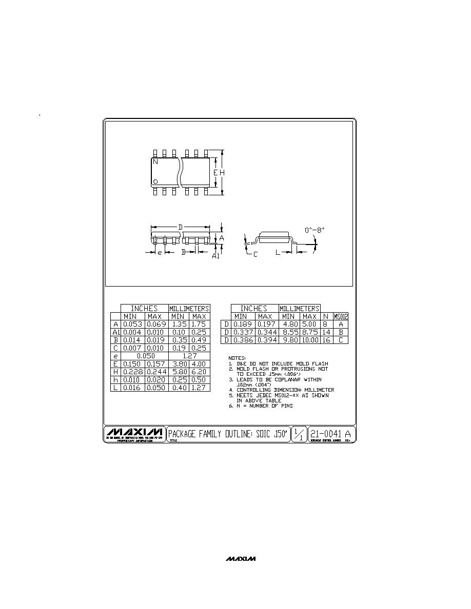
Package Information
SOT5L.EPS

MAX4249≠MAX4257
SOT23, Single-Supply, Low-Noise,
Low-Distortion, Rail-to-Rail Op Amps
______________________________________________________________________________________
15
___________________________________________Package Information (continued)
10LUMAXB.EPS
MAX4249≠MAX4257
SOT23, Single-Supply, Low-Noise,
Low-Distortion, Rail-to-Rail Op Amps
Maxim cannot assume responsibility for use of any circuitry other than circuitry entirely embodied in a Maxim product. No circuit patent licenses are
implied. Maxim reserves the right to change the circuitry and specifications without notice at any time.
16
____________________Maxim Integrated Products, 120 San Gabriel Drive, Sunnyvale, CA 94086 408-737-7600
© 1998 Maxim Integrated Products
Printed USA
is a registered trademark of Maxim Integrated Products.
___________________________________________Package Information (continued)
SOICN.EPS