_______________General Description
The MAX4158/MAX4159/MAX4258/MAX4259 are wide-
band, 2-channel, noninverting video amplifiers with input
multiplexing, capable of driving ±2.5V signals into 50
or
75
loads. These devices are current-mode feedback
amplifiers; gain is set by external feedback resistors. The
MAX4158/MAX4159 are optimized for unity gain (0dB)
with a -3dB bandwidth of 350MHz. The MAX4258/
MAX4259 are optimized for gains of two (6dB) or more
with a 250MHz -3dB bandwidth. These devices have low
(0.01%/0.01∞) differential gain and phase errors, and oper-
ate from ±5V supplies.
These devices are ideal for use in broadcast and graphics
video systems because of their low, 2pF input capaci-
tance, channel-to-channel switching time of only 20ns,
and wide, 130MHz 0.1dB bandwidth. In addition, the com-
bination of ultra-high speed and low power makes them
suitable for use in general-purpose high-speed applica-
tions, such as medical imaging, industrial instrumentation,
and communications systems.
The MAX4159/MAX4259 have address latching and high-
impedance output disabling, allowing them to be incorpo-
rated into large switching arrays. They are available in
14-pin SO and 16-pin QSOP packages. The MAX4158/
MAX4258 have no address latching or output disabling,
but are available in space-saving 8-pin µMAX and SO
packages.
________________________Applications
Video-Signal Multiplexing
Video Crosspoint Switches
Pixel Switching
Coaxial Cable Drivers
Workstations
High-Definition TV (HDTV)
Broadcast Video
Multimedia Products
High-Speed Signal Processing
____________________________Features
o
Excellent Video Specifications:
0.1dB Gain Flatness to 130MHz
0.01%/0.01∞ Differential Gain/Phase Error
o
High Speed:
350MHz -3dB Bandwidth (MAX4158/4159)
250MHz -3dB Bandwidth (MAX4258/4259)
700V/µs Slew Rate (MAX4158/4159)
1000V/µs Slew Rate (MAX4258/4259)
20ns Settling Time to 0.1%
o
Fast Switching:
20ns Channel-Switching Time
<70mV Switching Transient
o
Low Power: 100mW
o
Directly Drive 75
or 50
Cables
o
High Output Current Drive: >70mA
o
Address Latch and High-Z Output Disable
MAX4158/MAX4159/MAX4258/MAX4259
350MHz/250MHz, 2-Channel
Video Multiplexer-Amplifiers
________________________________________________________________
Maxim Integrated Products
1
19-1164; Rev 2; 3/01
______________Ordering Information
_________________Pin Configurations
PART
MAX4158
ESA
MAX4158EUA
MAX4159
ESD
MAX4159EEE
-40∞C to +85∞C
-40∞C to +85∞C
TEMP. RANGE
PIN-PACKAGE
8 SO
8 µMAX
-40∞C to +85∞C
-40∞C to +85∞C
14 SO
16 QSOP
MAX4258
ESA
MAX4258EUA
MAX4259
ESD
MAX4259EEE
-40∞C to +85∞C
-40∞C to +85∞C
8 SO
8 µMAX
-40∞C to +85∞C
-40∞C to +85∞C
14 SO
16 QSOP
MAX4158/MAX4258
A0
0
1
INPUT
MAX4158/MAX4258
IN0
IN1
V+
IN1
FB
V-
1
2
8
7
A0
OUT
GND
IN0
SO/
µ
MAX
TOP VIEW
3
4
6
5
Pin Configurations continued at end of data sheet.
EVALUATION KIT MANUAL
FOLLOWS DATA SHEET
For pricing, delivery, and ordering information, please contact Maxim/Dallas Direct! at
1-888-629-4642, or visit Maxim's website at www.maxim-ic.com.
MAX4158/MAX4159/MAX4258/MAX4259
350MHz/250MHz, 2-Channel
Video Multiplexer-Amplifiers
2
_______________________________________________________________________________________
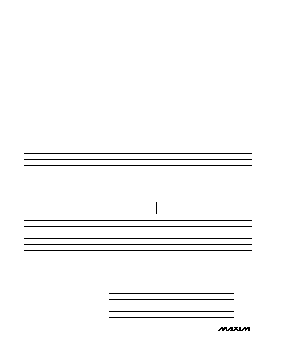
ABSOLUTE MAXIMUM RATINGS
DC ELECTRICAL CHARACTERISTICS
(V+ = +5V, V- = -5V, V
IN
= 0V, V
OUT
= 0V, R
L
=
, T
A
= T
MIN
to T
MAX
, unless otherwise noted. Typical values are at T
A
= +25∞C.)
Stresses beyond those listed under "Absolute Maximum Ratings" may cause permanent damage to the device. These are stress ratings only, and functional
operation of the device at these or any other conditions beyond those indicated in the operational sections of the specifications is not implied. Exposure to
absolute maximum rating conditions for extended periods may affect device reliability.
Note 1:
Continuous power dissipation maximum rating must also be observed.
Positive Supply Voltage (V+ to GND) ...................................+6V
Negative Supply Voltage (V- to GND).....................................-6V
Amplifier Input Voltage (IN0 or IN1) .....(V- - 0.3V) to (V+ + 0.3V)
FB Current ........................................................................±20mA
Digital Input Voltage (A0, EN, or LE) ............-0.3V to (V+ + 0.3V)
Output Short Circuit to GND (Note 1).........................Continuous
Output Short-Circuit Current to V+, V- (Note 1)........................5s
Continuous Power Dissipation (T
A
= +70∞C)
8-Pin SO (derate 5.88mW/∞C above +70∞C).................471mW
8-Pin µMAX (derate 4.10mW/∞C above +70∞C) ............330mW
14-Pin SO (derate 8.33mW/∞C above +70∞C)...............667mW
16-Pin QSOP (derate 8.33mW/∞C above +70∞C)..........667mW
Operating Temperature Range ...........................-40∞C to +85∞C
Storage Temperature Range .............................-65∞C to +160∞C
Lead Temperature (soldering, 10s) .................................+300∞C
Inferred from the CMRR test
Inferred from the PSRR test
V
OUT
= -2.5V to 2.5V
MAX4159/MAX4259 only, EN = 5V,
V
OUT
= -3.0V to 3.0V (Note 2)
f = 0Hz
R
L
= 50
R
L
= open circuit
V
IN
= -2.5V to 2.5V
T
A
= +25∞C
T
A
= +25∞C
V
IN
= -2.5V to 2.5V
V
OUT
= -2.5V to 2.5V, R
L
= 100
CONDITIONS
mA
70
100
I
OUT
Output Current
±2.5
±3.5
V
OUT
V
±3.0
±4.0
Output Voltage Swing
dB
50
60
CMRR
DC Common-Mode Rejection Ratio
M
1.0 3.0
Z
T
Open-Loop Transimpedance
mV
±1
±6
V
OS
Input Offset Voltage (Either Channel)
V
±2.5
±3.0
V
IN
V
±4.5 ±5.5
V+, V-
Operating Supply-Voltage Range
Input Voltage Range
M
1
10
R
OUT(d)
Disabled Output Resistance
m
40
R
OUT
Output Resistance
50
R
IN(FB)
FB Pin Input Resistance
M
1
20
R
IN
µV/∞C
2
TCV
OS
Input Offset Voltage Temperature
Coefficient (Either Channel)
µA
±2
±10
I
IN
Input Bias Current (Channel On)
µA
±2
±12
I
FB
FB Pin Bias Current
k
100
550
Input Resistance
UNITS
MIN
TYP
MAX
SYMBOL
PARAMETER
Channel on
Channel off
Open loop, V+ = +4.5V to +5.5V,
V- = -4.5V to -5.5V
dB
60
78
PSRR
DC Power-Supply Rejection Ratio
Sinking or sourcing to ground
mA
120
I
SC
Output Short-Circuit Current
MAX4158/MAX4258
10.9
13.0
EN = GND, MAX4159/MAX4259
10.9
13.0
EN = V+, MAX4159/MAX4259
mA
6.3
8.0
I+
Positive Supply Current
MAX4158/MAX4258
9.9
12.0
EN = GND, MAX4159/MAX4259
9.9
12.0
EN = V+, MAX4159/MAX4259
mA
5.0
7.0
I-
Negative Supply Current
T
A
= T
MIN
to T
MAX
T
A
= T
MIN
to T
MAX
±18
±20
MAX4158/MAX4159/MAX4258/MAX4259
350MHz/250MHz, 2-Channel
Video Multiplexer-Amplifiers
_______________________________________________________________________________________
3
DC ELECTRICAL CHARACTERISTICS (continued)
(V+ = +5V, V- = -5V, V
IN
= 0V, V
OUT
= 0V, R
L
=
, T
A
= T
MIN
to T
MAX
, unless otherwise noted. Typical values are at T
A
= +25∞C.)
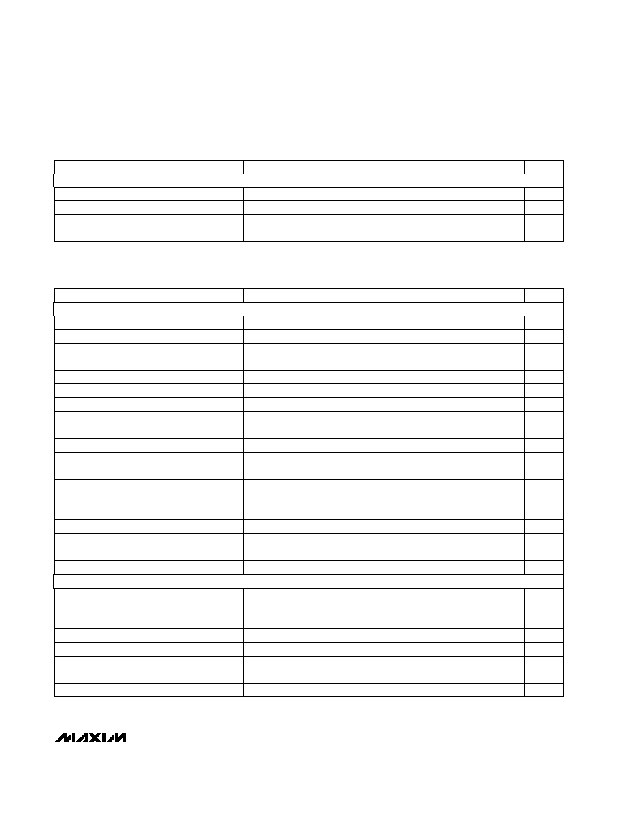
AC ELECTRICAL CHARACTERISTICS--MAX4158/MAX4159
(V+ = +5V, V- = -5V, V
IN
= 0V, V
OUT
= 0V, R
L
= 100
, T
A
= +25∞C, unless otherwise noted.)
V
IL
= 0
V
IH
= 5.5V, V+ = +5.5V
CONDITIONS
µA
130
300
I
IH
Logic-High Input Current
µA
-2
-20
I
IL
Logic-Low Input Current
V
2.0
V
IH
Logic-High Threshold
V
0.8
V
IL
Logic-Low Threshold
UNITS
MIN
TYP
MAX
SYMBOL
PARAMETER
A
V
= 0dB, V
OUT
= 2Vp-p (Note 4)
A
V
= 0dB, V
IN
= 20mVp-p (Note 4)
A
V
= 0dB, V
IN
= 20mVp-p (Note 4)
V
OUT
= 2V step, A
V
= 0dB (Note 4)
A
V
= 0dB, V
OUT
= 2Vp-p (Note 4)
CONDITIONS
ns
10
t
S
Settling Time to 0.1%
V/µs
700
SR
Slew Rate
MHz
155
FPBW
Full-Power Bandwidth
MHz
100
BW(0.1)
Bandwidth for ±0.1dB Gain Flatness
MHz
350
BW
-3dB Bandwidth
UNITS
MIN
TYP
MAX
SYMBOL
PARAMETER
A
V
= 0dB (Notes 4, 5)
%
0.01
DG
Differential Gain Error
f = 30MHz, V
OUT
= 2Vp-p,
A
V
= 0dB (Note 4)
f = 30MHz, A
V
= 0dB (Note 4)
f = 30MHz, R
S
= 50
, A
V
= 0dB,
V
IN
= ±2Vp-p (Note 4)
A
V
= 0dB (Notes 4, 5)
f = 30MHz, A
V
= 0dB, EN = 5V,
V
IN
= ±2Vp-p (Note 4)
pF
3
C
OUT
Output Capacitance
dB
105
A
ISO
Off-Isolation (MAX4159 only)
dBc
50
THD
Total Harmonic Distortion
9
Z
OUT
Output Impedance
dB
70
Xtalk
Channel-to-Channel Crosstalk
degrees
0.01
DP
Differential Phase Error
Channel on or off
pF
2
C
IN
Input Capacitance
f = 100kHz
f = 100kHz
f = 100kHz
pA/
Hz
22
i
n
(FB)
FB Current-Noise Density
pA/
Hz
2
i
n
Input Current-Noise Density
nV/
Hz
2
e
n
Input Voltage-Noise Density
(Notes 6, 7)
ns
20
t
SW
Channel Switching Time
T
A
= T
MIN
to T
MAX
(Notes 6, 8)
ns
10
t
S
Address Setup Time
(Note 6)
T
A
= T
MIN
to T
MAX
(Notes 6, 8)
ns
20
t
LPD
Latch Propagation Delay
ns
10
t
TH
Address Hold Time
T
A
= T
MIN
to T
MAX
(Notes 6, 8)
ns
10
t
LPW
Latch Pulse Width
(Notes 6, 9)
ns
20
t
PDE
Enable Delay Time
A
V
= 0dB (Notes 4, 10)
(Notes 6, 9)
mV
±70
V
TRAN
Switching Transient
ns
20
t
PDD
Disable Delay Time
LOGIC CHARACTERISTICS
(Note 3)
AMPLIFIER CHARACTERISTICS
SWITCHING CHARACTERISTICS

MAX4158/MAX4159/MAX4258/MAX4259
350MHz/250MHz, 2-Channel
Video Multiplexer-Amplifiers
4
_______________________________________________________________________________________
AC ELECTRICAL CHARACTERISTICS--MAX4258/MAX4259
(V+ = +5V, V- = -5V, V
IN
= 0V, V
OUT
= 0V, R
L
= 100
, T
A
= +25∞C, unless otherwise noted.)
f = 30MHz, V
OUT
= 2Vp-p,
A
V
= 6dB (Note 4)
f = 30MHz, A
V
= 6dB (Note 4)
f = 30MHz, R
S
= 50
, A
V
= 6dB,
V
IN
= ±1Vp-p (Note 4)
A
V
= 6dB (Notes 4, 5)
f = 30MHz, A
V
= 6dB, EN = 5V,
V
IN
= ±1Vp-p (Note 4)
pF
3
C
OUT
Output Capacitance
dB
110
A
V
= 6dB, V
OUT
= 2Vp-p (Note 4)
A
V
= 6dB, V
IN
= 20mVp-p (Note 4)
A
ISO
Off-Isolation (MAX4259)
A
V
= 6dB, V
IN
= 20mVp-p (Note 4)
dBc
50
THD
V
OUT
= 2V step, A
V
= 6dB (Note 4)
Total Harmonic Distortion
A
V
= 6dB, V
OUT
= 2Vp-p (Note 4)
CONDITIONS
9
Z
OUT
Output Impedance
dB
70
Xtalk
Channel-to-Channel Crosstalk
degrees
0.02
DP
Differential Phase Error
Channel on or off
pF
2
C
IN
Input Capacitance
f = 100kHz
f = 100kHz
f = 100kHz
pA/
Hz
22
i
n
(FB)
FB Current-Noise Density
pA/
Hz
2
i
n
Input Current-Noise Density
nV/
Hz
2
e
n
Input Voltage-Noise Density
(Notes 6, 7)
ns
20
t
SW
Channel-Switching Time
T
A
= T
MIN
to T
MAX
(Notes 6, 8)
ns
ns
10
t
S
Settling Time to 0.1%
V/µs
1000
SR
Slew Rate
10
t
S
Address-Setup Time
(Note 6)
T
A
= T
MIN
to T
MAX
(Notes 6, 8)
(Notes 6, 9)
ns
20
t
PDE
Enable Delay Time
A
V
= 6dB (Notes 4, 10)
(Notes 6, 9)
MHz
200
FPBW
Full-Power Bandwidth
MHz
130
BW(0.1)
Bandwidth for ±0.1dB Gain Flatness
MHz
250
BW
-3dB Bandwidth
mV
±90
V
TRAN
ns
20
t
LPD
Latch Propagation Delay
ns
10
t
TH
Address-Hold Time
T
A
= T
MIN
to T
MAX
(Notes 6, 8)
ns
10
t
LPW
Latch Pulse Width
UNITS
MIN
TYP
MAX
SYMBOL
PARAMETER
Switching Transient
ns
20
t
PDD
Disable Delay Time
A
V
= 6dB (Notes 4, 5)
%
0.01
DG
Differential Gain Error
Note 2:
Does not include external feedback network resistance.
Note 3:
Applies to all digital input pins (EN, LE, and A0).
Note 4:
Specified with feedback network chosen for optimal AC performance. See Tables 1 and 2 for recommended component
values.
Note 5:
Input test signal: 3.58MHz sine wave of amplitude 40IRE superimposed on a linear ramp (0IRE to 100IRE). IRE is a unit of
video-signal amplitude developed by the International Radio Engineers. 140IRE = 1.0V.
Note 6:
See timing diagram (Figure 5).
Note 7:
Channel-switching time specified for switching between the two input channels; does not include signal rise/fall times for
switching between channels with different input voltages.
Note 8:
Guaranteed by design; not production tested.
Note 9:
Output enable/disable delay times do not include amplifier output slewing times.
Note 10:
Switching transient measured while switching between two grounded channels.
AMPLIFIER CHARACTERISTICS
SWITCHING CHARACTERISTICS
MAX4158/MAX4159/MAX4258/MAX4259
350MHz/250MHz, 2-Channel
Video Multiplexer-Amplifiers
_______________________________________________________________________________________
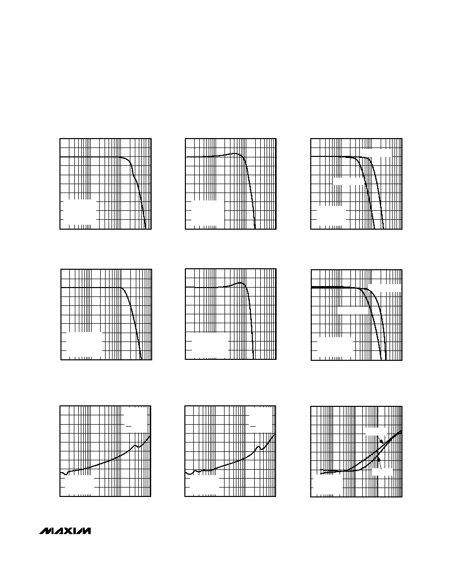
5
2
-8
1
10
100
1000
MAX4158/MAX4159
SMALL-SIGNAL FREQUENCY RESPONSE
-4
-6
0
-2
MAX4158/59-01
FREQUENCY (MHz)
GAIN (dB)
V
IN
= 20mVp-p
A
V
= +1V/V
R
F
= 430
R
L
= 100
0.2
-0.8
1
10
100
1000
MAX4158/MAX4159
GAIN FLATNESS vs. FREQUENCY
-0.4
-0.6
0
-0.2
MAX4158/59-02
FREQUENCY (MHz)
GAIN (dB)
V
IN
= 20mVp-p
A
V
= +1V/V
R
F
= 430
R
L
= 100
2
-8
1
10
100
1000
MAX4158/MAX4159
LARGE-SIGNAL FREQUENCY RESPONSE
-4
-6
0
-2
MAX4158/59-03
FREQUENCY (MHz)
GAIN (dB)
A
V
= +1V/V
R
F
= 430
R
L
= 100
2Vp-p OUTPUT
4Vp-p OUTPUT
8
-2
1
10
100
1000
MAX4258/MAX4259
SMALL-SIGNAL FREQUENCY RESPONSE
2
0
6
4
MAX4158/59-04
FREQUENCY (MHz)
GAIN (dB)
V
IN
= 20mVp-p
A
V
= +2V/V
R
F
= R
G
= 510
R
L
= 100
20
-180
1
10
100
1000
MAX4159
OFF ISOLATION vs. FREQUENCY
-80
-100
-120
-140
-160
-20
0
-60
-40
MAX4158/59-07a
FREQUENCY (MHz)
GAIN (dB)
A
V
= +1V/V
R
L
= 100
R
F
= 430
IN0 = ±2V
IN1 = GND
A0 = GND
EN = 5V
6.2
5.2
1
10
100
1000
MAX4258/MAX4259
GAIN FLATNESS vs. FREQUENCY
5.6
5.4
6.0
5.8
MAX4158/59-05
FREQUENCY (MHz)
GAIN (dB)
V
IN
= 20mVp-p
A
V
= +2V/V
R
F
= R
G
= 510
R
L
= 100
8
-2
1
10
100
1000
MAX4258/MAX4259
LARGE-SIGNAL FREQUENCY RESPONSE
2
0
6
4
MAX4158/59-06
FREQUENCY (MHz)
GAIN (dB)
A
V
= +2V/V
R
F
= R
G
= 510
R
L
= 100
2Vp-p OUTPUT
4Vp-p OUTPUT
20
-180
1
10
100
1000
MAX4259
OFF ISOLATION vs. FREQUENCY
-80
-100
-120
-140
-160
-20
0
-60
-40
MAX4158/59-07b
FREQUENCY (MHz)
GAIN (dB)
A
V
= +2V/V
R
L
= 100
R
F
= R
G
= 510
IN0 = ±1V
IN1 = GND
A0 = GND
EN = 5V
10
-90
0.1
0.01
1
10
100
MAX4158/MAX4159
POWER-SUPPLY REJECTION RATIO
vs. FREQUENCY
-40
-50
-60
-70
-80
-10
0
-30
-20
MAX4158/59-08
FREQUENCY (MHz)
PSRR (dB)
A
V
= +1V/V
R
L
= 100
R
F
= 430
PSRR(+)
PSRR(-)
__________________________________________Typical Operating Characteristics
(V+ = +5V, V- = -5V, T
A
= +25∞C, unless otherwise noted.)